• Photonics Research
  • Vol. 9, Issue 4, 615 (2021)
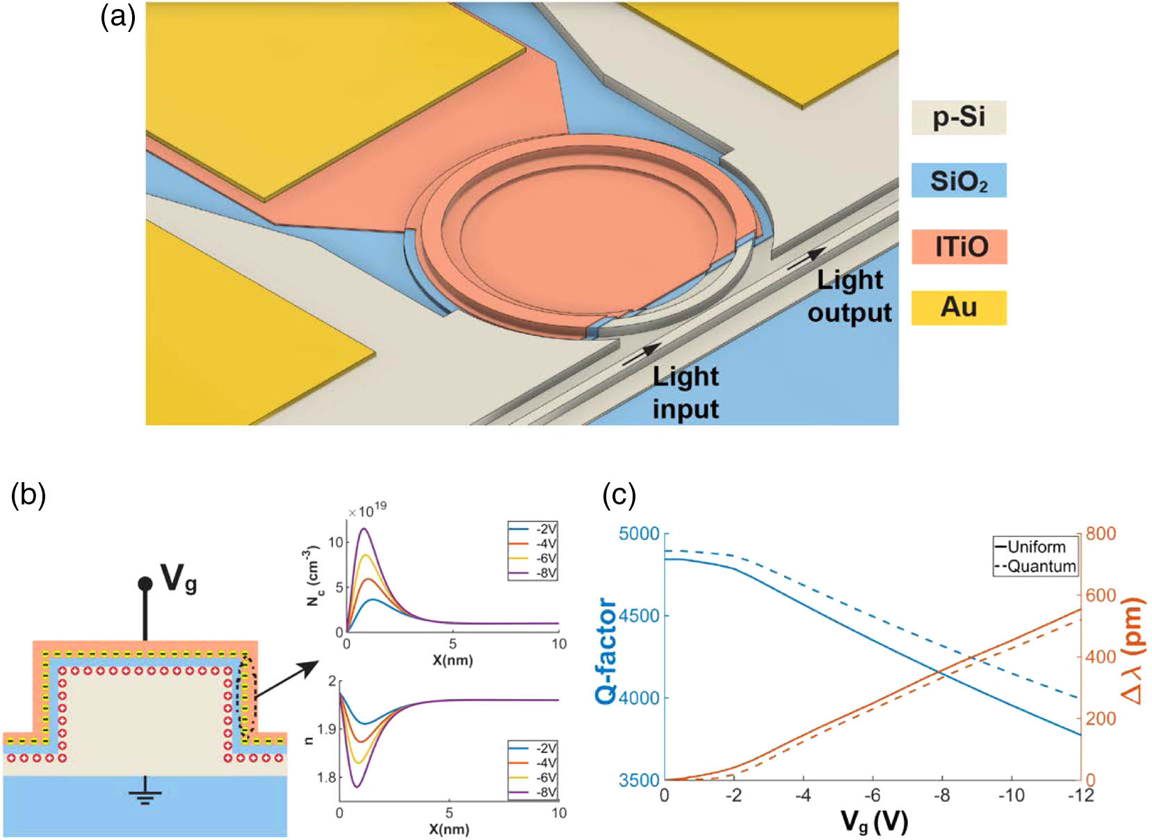
Wei-Che Hsu, Erwen Li, Bokun Zhou, and Alan X. Wang*
Author Affiliations
  • School of Electrical Engineering and Computer Science, Oregon State University, Corvallis, Oregon 97331, USA
  • show less
    DOI: 10.1364/PRJ.416656 Cite this Article Set citation alerts
    Wei-Che Hsu, Erwen Li, Bokun Zhou, Alan X. Wang. Characterization of field-effect mobility at optical frequency by microring resonators[J]. Photonics Research, 2021, 9(4): 615 Copy Citation Text show less
    (a) 3D schematic of ITiO-Si-SiO2 MOS-driven MRR. (b) Cross-sectional schematic in the active region. With the negative Vg, it induces the carrier accumulation and refractive index modulation in the ITiO and Si layers. (c) Simulated results with different models: quantum-moment model plots in dashed lines and uniform model plots in solid lines. Q factor (blue line, left y axis) and resonance wavelength shift Δλ (red line, right y axis) as a function of Vg.
    Fig. 1. (a) 3D schematic of ITiO-Si-SiO2 MOS-driven MRR. (b) Cross-sectional schematic in the active region. With the negative Vg, it induces the carrier accumulation and refractive index modulation in the ITiO and Si layers. (c) Simulated results with different models: quantum-moment model plots in dashed lines and uniform model plots in solid lines. Q factor (blue line, left y axis) and resonance wavelength shift Δλ (red line, right y axis) as a function of Vg.
    (a) Simulation model includes the p-Si layer, SiO2 layer, and the ITiO, consisting of the bulk material and 1 nm accumulation channel. (b) Simulated cross-sectional electric field intensity (|E|2) distribution of the ITiO-gated MOS bending waveguide with a 17 nm SiO2 layer and a 17 nm ITiO layer. (c) Q factor maps, with respect to μop,FE and Δλ, in different bulk conditions.
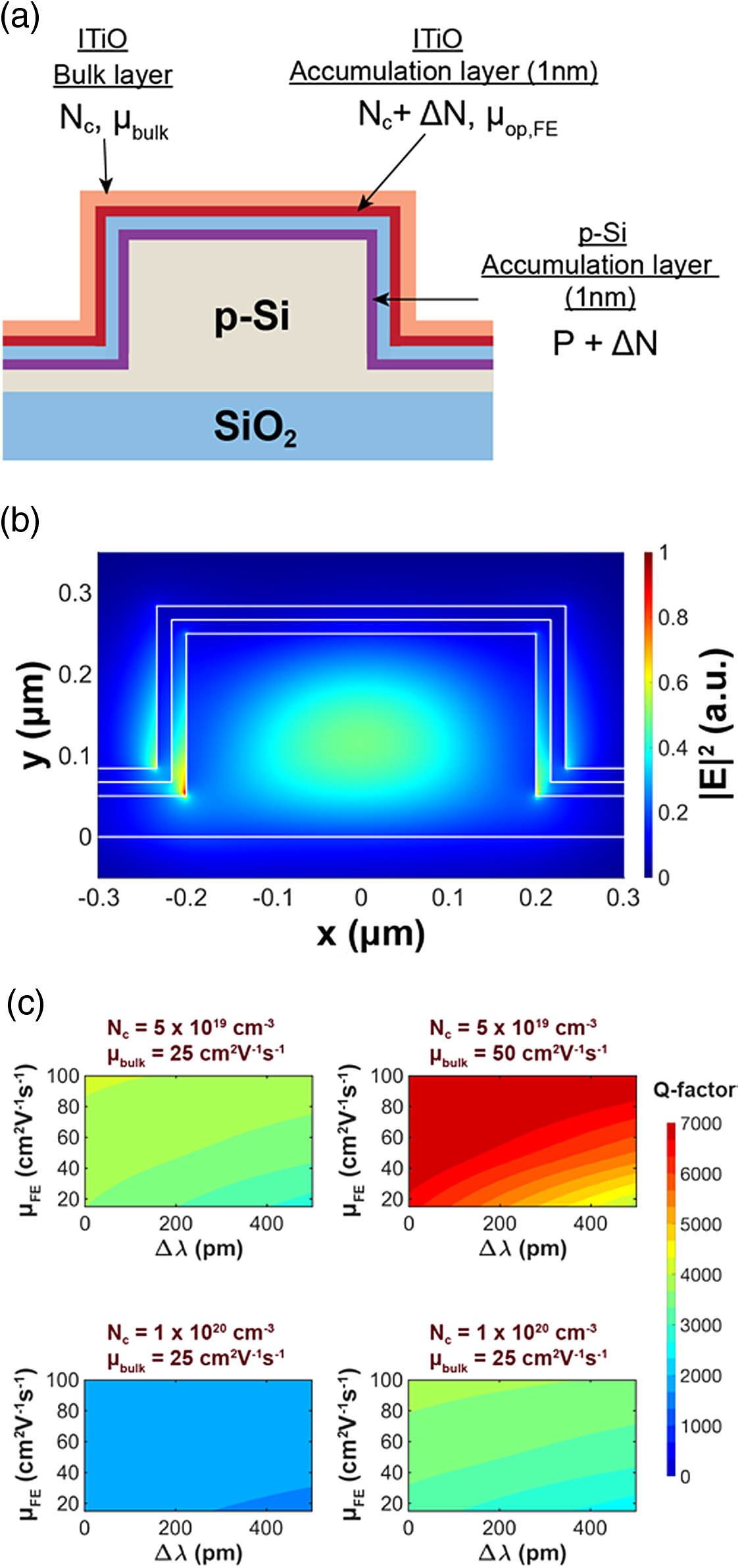
    Fig. 2. (a) Simulation model includes the p-Si layer, SiO2 layer, and the ITiO, consisting of the bulk material and 1 nm accumulation channel. (b) Simulated cross-sectional electric field intensity (|E|2) distribution of the ITiO-gated MOS bending waveguide with a 17 nm SiO2 layer and a 17 nm ITiO layer. (c) Q factor maps, with respect to μop,FE and Δλ, in different bulk conditions.
    (a) Scanning electron microscope (SEM) image of the fabricated passive Si-MRR with false colors. The microring has a radius of 6 μm. (b) Zoom-in SEM image of microring to show the side-wall roughness. (c) The experimental transmission spectrum of the passive MRR, which is fitted by the Lorentzian function, has a high Q factor of ∼13,000. (d) Optical image of the fabricated ITiO-gated MOS MRR. The ITiO gate, which is highlighted by the white dashed line, covers the active region of the microring except the coupling region to the bus waveguide. The active region covers ∼83% of the MRR. The gate electrode lies on ITiO, and the ground electrodes are connected to the p-Si microring through a partially etched Si slab.
    Fig. 3. (a) Scanning electron microscope (SEM) image of the fabricated passive Si-MRR with false colors. The microring has a radius of 6 μm. (b) Zoom-in SEM image of microring to show the side-wall roughness. (c) The experimental transmission spectrum of the passive MRR, which is fitted by the Lorentzian function, has a high Q factor of 13,000. (d) Optical image of the fabricated ITiO-gated MOS MRR. The ITiO gate, which is highlighted by the white dashed line, covers the active region of the microring except the coupling region to the bus waveguide. The active region covers 83% of the MRR. The gate electrode lies on ITiO, and the ground electrodes are connected to the p-Si microring through a partially etched Si slab.
    (a) Lorentzian fitted experimental transmission spectra of ITiO-gated MOS MRR with different Vg. (b) Experimental Q factor (blue line, left y axis) and Δλ (red line, right y axis). (c) μop,FE extraction from experimental Q factor and Δλ with errors. (d) Capacitance as a function of Vg for the ITiO-gated MOS MRR.
    Fig. 4. (a) Lorentzian fitted experimental transmission spectra of ITiO-gated MOS MRR with different Vg. (b) Experimental Q factor (blue line, left y axis) and Δλ (red line, right y axis). (c) μop,FE extraction from experimental Q factor and Δλ with errors. (d) Capacitance as a function of Vg for the ITiO-gated MOS MRR.
    Wei-Che Hsu, Erwen Li, Bokun Zhou, Alan X. Wang. Characterization of field-effect mobility at optical frequency by microring resonators[J]. Photonics Research, 2021, 9(4): 615
    Download Citation