
Wei-Che Hsu, Erwen Li, Bokun Zhou, Alan X. Wang, "Characterization of field-effect mobility at optical frequency by microring resonators," Photonics Res. 9, 615 (2021)
- Photonics Research
- Vol. 9, Issue 4, 615 (2021)
Abstract
1. INTRODUCTION
Metal–oxide–semiconductor (MOS) capacitors are one of the most prevailing electronic device structures, and have laid the foundation of modern transistors that have transformed the entire industry of microelectronics [1]. In recent years, MOS devices have also gained increasing utility in photonic applications, which could pave the way for a new generation of hybrid electronic–photonic systems [2,3]. MOS-driven silicon photonic devices in particular have rapidly become one of the most promising building blocks for future optical interconnect systems due to their enhanced performance in electro-optic (E-O) modulation and scalability of fabrication [4–6]. Photonic devices based on the MOS structure usually operate in the accumulation mode. When a negative bias voltage (
Carrier mobility is one of the most pivotal properties of semiconductors, as it can determine the performance of solid-state devices. Carrier mobility represents the velocity of electrons or holes under certain electric fields, and therefore it determines the conductivity and frequency response of electronic devices such as transistors. Thus, the high mobility of semiconductors is critical to achieving high bandwidth and low power dissipation [14]. For photonic devices, the impact of carrier mobility reaches even further. As described by the Drude model, the collision frequency [Eq. (1c)], which is the collision process between free carriers and ionized impurities in TCOs, is inversely proportional to the carrier mobility at the optical frequency [15,16]. Furthermore, the optical loss due to free carrier absorption is determined by the imaginary part of the complex permittivity [Eq. (1a)], which is influenced by the collision frequency as well. Hence, high-mobility semiconductors are critical to low optical loss waveguides. For instance, previous research has shown that high-mobility TCOs can significantly enhance the performance of photonic modulators by increasing the extinction ratio, improving the energy efficiency and quality factor (
The carrier mobility of semiconductors at electrical frequency (DC or RF) is usually measured by the Hall effect. It actually measures the bulk mobility (
Sign up for Photonics Research TOC. Get the latest issue of Photonics Research delivered right to you!Sign up now
In contrast to electric frequency mobility, which is limited by ionized-impurity scattering and grain-boundary scattering, the optical frequency mobility (
In this paper, we propose a novel characterization method to extract the
2. DESIGN AND PRINCIPLE
A. Design of ITiO-gated MOS MRR
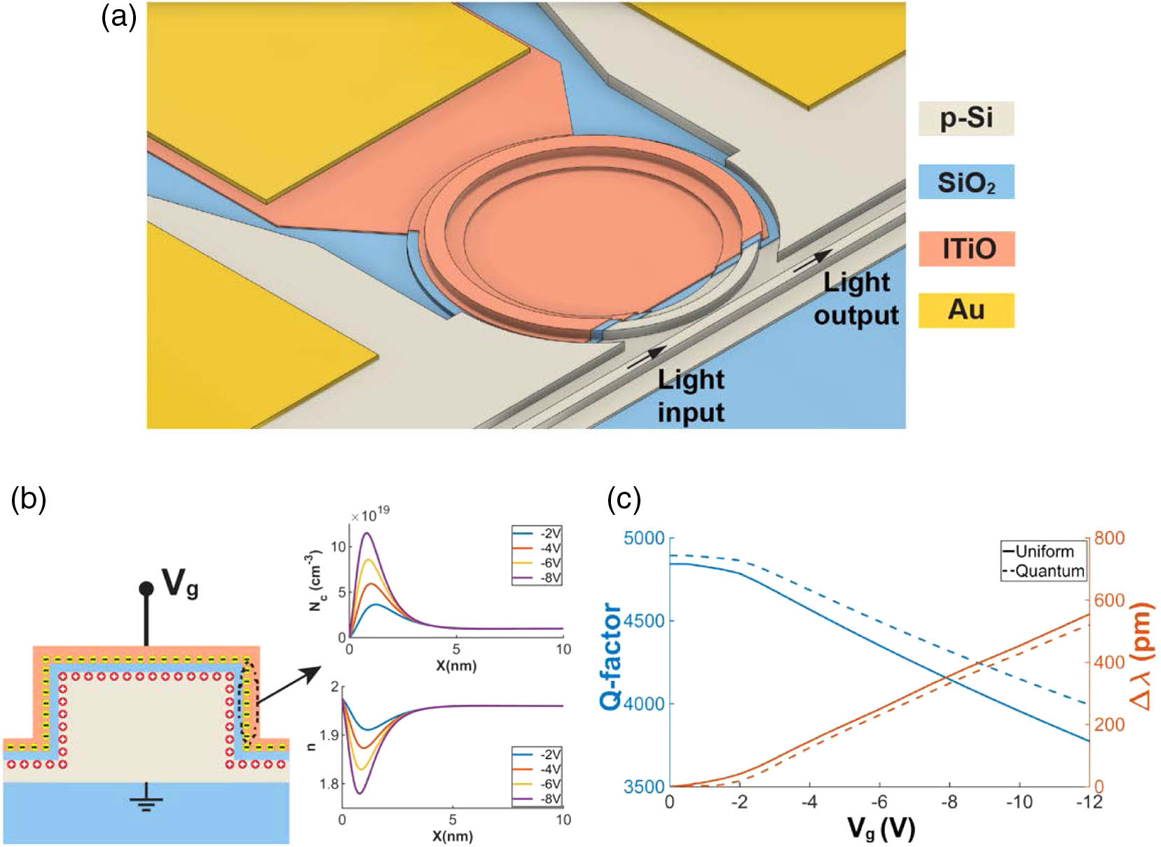
Figure 1.(a) 3D schematic of
The plasma frequency (
The plasma collision frequency (
The value of
The
As shown in Fig. 1(a), the ITiO does not cover the whole ring. Therefore, the
To understand how the
B. Model Setup
![]()
Figure 2.(a) Simulation model includes the p-Si layer,
When a negative
3. FABRICATION AND CHARACTERIZATION
A. Fabrication Processes and Testing
![]()
Figure 3.(a) Scanning electron microscope (SEM) image of the fabricated passive Si-MRR with false colors. The microring has a radius of 6 μm. (b) Zoom-in SEM image of microring to show the side-wall roughness. (c) The experimental transmission spectrum of the passive MRR, which is fitted by the Lorentzian function, has a high
Next, a 17 nm thick
B. Experimental Results
In this work, the initial condition of ITiO is measured, which has the
![]()
Figure 4.(a) Lorentzian fitted experimental transmission spectra of ITiO-gated MOS MRR with different
Since this method is an indirect method to estimate the
4. CONCLUSION
In conclusion, we invented a new characterization method for quantifying the
Acknowledgment
Acknowledgment. The authors would like to acknowledge the Oregon State University Materials Synthesis and Characterization Facility (MASC) and Electronic Microscopy Facility for their support in device fabrication, and Prof. Janet Tate at the Department of Physics for the Hall measurement.
References
[1] C. T. Sah. Evolution of the MOS transistor-from conception to VLSI. Proc. IEEE, 76, 1280-1326(1988).
[2] H. C. Lin, W. E. Wang, G. Brammertz, M. Meuris, M. Heyns. Electrical study of sulfur passivated In0.53Ga0.47As MOS capacitor and transistor with ALD Al2O3 as gate insulator. Microelectron. Eng., 86, 1554-1557(2009).
[3] M. K. Kim, J. S. Lee. Synergistic improvement of long-term plasticity in photonic synapses using ferroelectric polarization in hafnia-based oxide-semiconductor transistors. Adv. Mater., 32, 1907826(2020).
[4] A. Liu, R. Jones, L. Liao, D. Samara-Rubio, D. Rubin, O. Cohen, R. Nicolaescu, M. Paniccia. A high-speed silicon optical modulator based on a metal-oxide-semiconductor capacitor. Nature, 427, 615-618(2004).
[5] W. Cai, J. S. White, M. L. Brongersma. Power-efficient electrooptic plasmonic modulators. Nano Lett., 9, 4403-4411(2009).
[6] K. Debnath, D. J. Thomson, W. Zhang, A. Z. Khokhar, C. Littlejohns, J. Byers, L. Mastronardi, M. K. Husain, K. Ibukuro, F. Y. Gardes, G. T. Reed, S. Saito. All-silicon carrier accumulation modulator based on a lateral metal-oxide-semiconductor capacitor. Photon. Res., 6, 373-379(2018).
[7] M. Midrio, P. Galli, M. Romagnoli, L. C. Kimerling, J. Michel. Graphene-based optical phase modulation of waveguide transverse electric modes. Photon. Res., 2, A34-A40(2014).
[8] J. H. Han, F. Boeuf, J. Fujikata, S. Takahashi, S. Takagi, M. Takenaka. Efficient low-loss InGaAsP/Si hybrid MOS optical modulator. Nat. Photonics, 11, 486-490(2017).
[9] R. Amin, R. Maiti, C. Carfano, Z. Ma, M. H. Tahersima, Y. Lilach, D. Ratnayake, H. Dalir, V. J. Sorger. 0.52 V mm ITO-based Mach-Zehnder modulator in silicon photonics. APL Photon., 3, 126104(2018).
[10] E. Feigenbaum, K. Diest, H. A. Atwater. Unity-order index change in transparent conducting oxides at visible frequencies. Nano Lett., 10, 2111-2116(2010).
[11] Q. Gao, E. Li, A. X. Wang. Ultra-compact and broadband electro-absorption modulator using an epsilon-near-zero conductive oxide. Photon. Res., 6, 277-281(2018).
[12] E. Li, Q. Gao, S. Liverman, A. X. Wang. One-volt silicon photonic crystal nanocavity modulator with indium oxide gate. Opt. Lett., 43, 4429-4432(2018).
[13] E. Li, B. A. Nia, B. Zhou, A. X. Wang. Transparent conductive oxide-gated silicon microring with extreme resonance wavelength tunability. Photon. Res., 7, 473-477(2019).
[14] S. H. Mir, V. K. Yadav, J. K. Singh, J. K. Singh. Recent advances in the carrier mobility of two-dimensional materials: a theoretical perspective. ACS Omega, 5, 14203-14211(2020).
[15] S. D’Elia, N. Scaramuzza, F. Ciuchi, C. Versace, G. Strangi, R. Bartolino. Ellipsometry investigation of the effects of annealing temperature on the optical properties of indium tin oxide thin films studied by Drude-Lorentz model. Appl. Surf. Sci., 255, 7203-7211(2009).
[16] J. Ederth, A. Hultåker, G. A. Niklasson, P. Heszler, A. R. Van Doorn, M. J. Jongerius, D. Burgard, C. G. Granqvist. Thin porous indium tin oxide nanoparticle films: effects of annealing in vacuum and air. Appl. Phys. A, 81, 1363-1368(2005).
[17] S. Campione, M. G. Wood, D. K. Serkland, S. Parameswaran, J. Ihlefeld, T. S. Luk, J. R. Wendt, K. M. Geib, G. A. Keeler. Submicrometer epsilon-near-zero electroabsorption modulators enabled by high-mobility cadmium oxide. IEEE Photon. J., 9, 2723299(2017).
[18] B. Zhou, E. Li, Y. Bo, A. Wang. High-speed plasmonic-silicon modulator driven by epsilon-near-zero conductive oxide. J. Lightwave Technol., 38, 3338-3345(2020).
[19] T. I. Kamins. Hall mobility in chemically deposited polycrystalline silicon. J. Appl. Phys., 42, 4357-4365(1971).
[20] Y. Sago, H. Fujiwara. Mapping characterization of SnO2:F transparent conductive oxide layers by ellipsometry technique. Jpn. J. Appl. Phys., 51, 10NB01(2012).
[21] Z. Ma, Z. Li, K. Liu, C. Ye, V. J. Sorger. Indium-tin-oxide for high-performance electro-optic modulation. Nanophotonics, 4, 198-213(2015).
[22] K. I. Goto, T. H. Yu, J. Wu, C. H. Diaz, J. P. Colinge. Mobility and screening effect in heavily doped accumulation-mode metal-oxide-semiconductor field-effect transistors. Appl. Phys. Lett., 101, 073503(2012).
[23] J. F. Wager, D. A. Keszler, R. E. Presley. Transparent Electronics(2008).
[24] R. L. Huffman. ZnO-channel thin-film transistors: channel mobility. J. Appl. Phys., 95, 5813-5819(2004).
[25] Y. Nitzan, M. Grinshpan, Y. Goldstein. Field-effect mobility in quantized accumulation layers on ZnO surfaces. Phys. Rev. B, 19, 4107-4115(1979).
[26] C. J. Chiu, S. P. Chang, S. J. Chang. Transistor using Ta2O5 gate dielectric. IEEE Electron Device Lett., 31, 1245-1247(2010).
[27] Y. Chen, D. Geng, M. Mativenga, H. Nam, J. Jang. High-speed pseudo-CMOS circuits using bulk accumulation a-IGZO TFTs. IEEE Electron Device Lett., 36, 153-155(2015).
[28] Y. Shin, S. T. Kim, K. Kim, M. Y. Kim, S. Oh, J. K. Jeong. The mobility enhancement of indium gallium zinc oxide transistors via low-temperature crystallization using a tantalum catalytic layer. Sci. Rep., 7, 10885(2017).
[29] J. Steinhauser, S. Faÿ, N. Oliveira, E. Vallat-Sauvain, C. Ballif. Transition between grain boundary and intragrain scattering transport mechanisms in boron-doped zinc oxide thin films. Appl. Phys. Lett., 90, 142107(2007).
[30] H. C. M. Knoops, B. W. H. van de Loo, S. Smit, M. V. Ponomarev, J.-W. Weber, K. Sharma, W. M. M. Kessels, M. Creatore. Optical modeling of plasma-deposited ZnO films: electron scattering at different length scales. J. Vac. Sci. Technol. A, 33, 021509(2015).
[31] H. Fujiwara, M. Kondo. Effects of carrier concentration on the dielectric function of ZnO:Ga and In2O3:Sn studied by spectroscopic ellipsometry: analysis of free-carrier and band-edge absorption. Phys. Rev. B, 71, 075109(2005).
[32] G. V. Naik, V. M. Shalaev, A. Boltasseva. Alternative plasmonic materials: beyond gold and silver. Adv. Mater., 25, 3264-3294(2013).
[33] W. Bogaerts, P. de Heyn, T. van Vaerenbergh, K. de Vos, S. Kumar Selvaraja, T. Claes, P. Dumon, P. Bienstman, D. van Thourhout, R. Baets. Silicon microring resonators. Laser Photon. Rev., 6, 47-73(2012).
[34] W. Shi, X. Wang, W. Zhang, H. Yun, C. Lin, L. Chrostowski, N. A. F. Jaeger. Grating-coupled silicon microring resonators. Appl. Phys. Lett., 100, 121118(2012).
[35] J. Xie, L. Zhou, X. Sun, Z. Zou, L. Lu, H. Zhu, X. Li, J. Chen. Selective excitation of microring resonances using a pulley-coupling structure. Appl. Opt., 53, 878-884(2014).
[36] I. Demirtzioglou, C. Lacava, K. R. H. Bottrill, D. J. Thomson, G. T. Reed, D. J. Richardson, P. Petropoulos. Frequency comb generation in a silicon ring resonator modulator. Opt. Express, 26, 790-796(2018).
[37] X. Cheng, J. Hong, A. M. Spring, S. Yokoyama. Fabrication of a high-Q factor ring resonator using LSCVD deposited Si3N4 film. Opt. Mater. Express, 7, 2182-2187(2017).
[38] Q. Gao, E. Li, A. X. Wang. Comparative analysis of transparent conductive oxide electro-absorption modulators [Invited]. Opt. Mater. Express, 8, 2850-2862(2018).
[39] E. Li, Q. Gao, R. T. Chen, A. X. Wang. Ultracompact silicon-conductive oxide nanocavity modulator with 0.02 lambda-cubic active volume. Nano Lett., 18, 1075-1081(2018).
[40] A. Zeumault, V. Subramanian. Improved technique for quantifying the bias-dependent mobility of metal-oxide thin-film transistors. IEEE Trans. Electron Devices, 62, 855-861(2015).
[41] A. Zeumault, V. Subramanian. Mobility enhancement in solution-processed transparent conductive oxide TFTs due to electron donation from traps in high-


Set citation alerts for the article
Please enter your email address

© Copyright 2018-2021 | Chinese Laser Press. All Rights Reserved 沪ICP备15018463号-20