Yaoyuan Lei, Qikai Chen, Yitian Liu, Yaoguang Ma. Principles and application progress of mid-infrared metasurfaces in imaging and detection (Invited)[J]. Infrared and Laser Engineering, 2022, 51(3): 20220082
Search by keywords or author
- Infrared and Laser Engineering
- Vol. 51, Issue 3, 20220082 (2022)
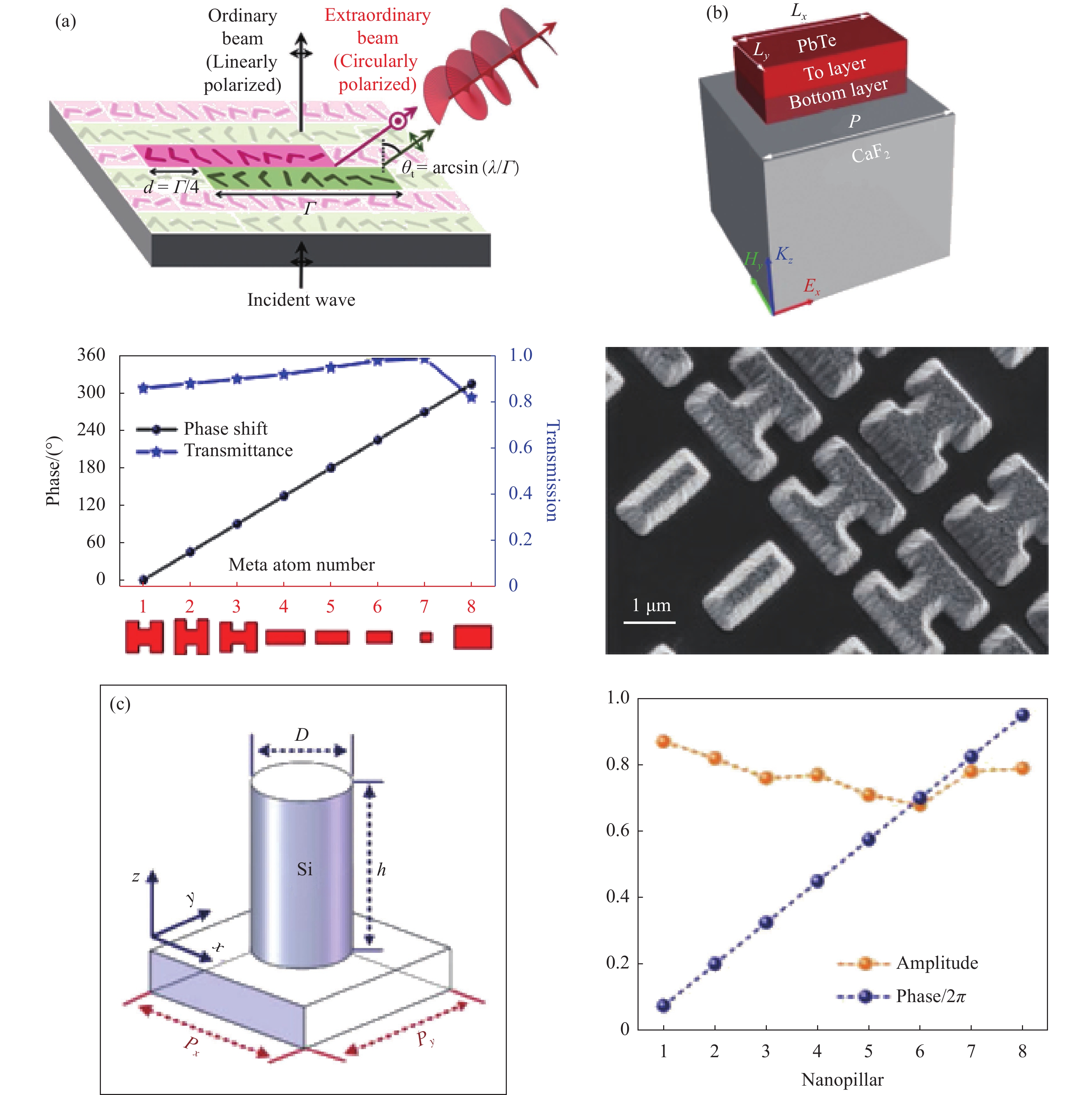
![Mid-infrared metasurface structures based on different electromagnetic wave control mechanism. (a) Metasurface quarter-wave plate based on the V-shaped antenna[44]; (b) Dielectric Huygens metasurface operating near the mid-IR wavelength of 5.2 µm, schematic tilted view of a rectangular meta-atom structure, the phase shift and transmittance corresponding to the eight meta-atom elements used to construct the meta-optical device, and the scanning electron microscope image of the fabricated metasurface structure, respectively[51]; (c) Long-wavelength infrared metalens composed of silicon nanopillars arranged on a square lattice. The building block of all-silicon metalens (left) and simulated amplitude and phase for eight selected nanopillars (right)[31]](/richHtml/irla/2022/51/3/20220082/img_1.jpg)
Fig. 1. Mid-infrared metasurface structures based on different electromagnetic wave control mechanism. (a) Metasurface quarter-wave plate based on the V-shaped antenna[44]; (b) Dielectric Huygens metasurface operating near the mid-IR wavelength of 5.2 µm, schematic tilted view of a rectangular meta-atom structure, the phase shift and transmittance corresponding to the eight meta-atom elements used to construct the meta-optical device, and the scanning electron microscope image of the fabricated metasurface structure, respectively[51]; (c) Long-wavelength infrared metalens composed of silicon nanopillars arranged on a square lattice. The building block of all-silicon metalens (left) and simulated amplitude and phase for eight selected nanopillars (right)[31]
![Mid-infrared polarization devices. (a) Schematic illustration of the BAFOV generation with polarization-dependent functions (left). The birefringent meta-atoms are made of monocrystalline Si (right)[69]; (b) Schematic of the GIAM-based polarimeter[71]; (c) Schematic of the Mid-IR full-Stokes polarization detection device design with seven cells for direct Stokes parameter measurement[73]](/richHtml/irla/2022/51/3/20220082/img_2.jpg)
Fig. 2. Mid-infrared polarization devices. (a) Schematic illustration of the BAFOV generation with polarization-dependent functions (left). The birefringent meta-atoms are made of monocrystalline Si (right)[69]; (b) Schematic of the GIAM-based polarimeter[71]; (c) Schematic of the Mid-IR full-Stokes polarization detection device design with seven cells for direct Stokes parameter measurement[73]
Fig. 3. GST phase-change material metasurfaces. (a) Sketch of the switchable perfect absorber device (left) and measured reflection spectra in amorphous and crystalline conditions for different antenna sizes (right)[36]; (b) Active plasmonic metasurface for beam switching (left) and experimental results for the cylindrical bifocal lens (right)[84]; (c) Artistic rendering of a reconfigurable varifocal metalens (left) and well-resolved lines of USAF-1951 resolution charts (right)[90]
Fig. 4. Graphene electrically tunable metasurfaces. (a) Mid-infrared optical modulator based on an electrically tunable metasurface absorber[35]. Schematic of the ultrathin optical modulator based on a tunable metasurface absorber and a scanning electron microscope (SEM) image of the metasurface on graphene (left). Measured reflection spectra from the metasurface absorber for different gate voltages (right); (b) The gate-tunable graphene-gold reconfigurable mid-infrared metasurface[92]. Schematic of a gate-tunable device for control of reflected phase and SEM image of gold resonators on graphene (left). The scale bar indicates 1 μm. Phase modulation at wavelengths of 8.2 µm, 8.5 µm, and 8.7 µm (circles-experiment, line-simulation) (right); (c) Hybrid graphene metasurface allows for electrically tunable resonant absorption[95]. Schematic of the hybrid graphene metasurface (left) and measured reflection spectra when applying different gate voltages (right)
Fig. 5. A schematic of the substrate prior to stretching with Au split ring resonators attached and a schematic of a stretched array (Top); The measured reflectance spectra and representative environmental scanning electron microscope (ESEM) images for the double SRR array for various degrees of strain (bottom)[77]
Fig. 6. Metal-based metasurfaces for surface enhanced infrared absorption. (a) Chemically specific, label-free nanophotonic biosensor in the mid-infrared[16]; (b) MOF-SEIRA platform for simultaneous sensing of CO2 and CH4 gases[21]
Fig. 7. Graphene metasurfaces for surface-enhanced infrared absorption. (a) Schematic of graphene plasmon enhanced molecular fingerprint sensor[117]; (b) Experimental scheme of the graphene plasmon device for gas identification[20]
Fig. 8. Molecular fingerprint retrieval and spatial absorption mapping of a mid-IR nanophotonic sensor based on all-dielectric high-Q metasurface elements[120]

Set citation alerts for the article
Please enter your email address


