
Xingwang Chen, Lei Chen, Ying Wang, Tao Wei, Jing Hu, Miao Cheng, Qianqian Liu, Wanfei Li, Yun Ling, Bo Liu, "AgGeSbTe thin film as a negative heat-mode resist for dry lithography," Chin. Opt. Lett. 20, 031601 (2022)
- Chinese Optics Letters
- Vol. 20, Issue 3, 031601 (2022)
Abstract
1. Introduction
Laser heat-mode lithography has a promising prospect in the optoelectronic region due to its high resolution, low cost, facile fabrication process, and so forth[
On the other hand, various heat-mode resists have been found for lithography such as organic polymers[
However, wet development is adopted in heat-mode lithography, which readily results in the undercut of resist and, therefore, the pattern collapse[
Sign up for Chinese Optics Letters TOC. Get the latest issue of Chinese Optics Letters delivered right to you!Sign up now
2. Experimental Details
AgGeSbTe films with the thickness of 250 nm were prepared onto silicon substrates according to the co-sputtering technique with Ag and
Atomic force microscopy (AFM) was utilized to determine the sample height information, where the instrument type was Nanosurf Core AFM, Switzerland. The scanning electron microscope (SEM, JSM-IT100) and transmission electron microscope (TEM, Tecnai G2 F20 S-TWIN) were used to observe cross-section profiles and surface morphologies. The composition ratio of AgGeSbTe resist was characterized via energy-dispersive X-ray spectroscopy (EDS), where the atomic fractions of Ag, Ge, Sb, and Te were 34.9%, 20.4%, 13.9%, and 30.8%, respectively. The crystallization temperature of AgGeSbTe was determined via the dependence of resistance on temperature measured by LINKAM HFS600E-PB4 hot stage. The crystal structures of the exposed samples were analyzed by an X-ray diffractometer of Bruker advance D8, Germany. The bonding environments of resists were measured according to the Raman spectroscopy (HORIBA LabRAM HR Evolution, laser wavelength of 532 nm) and X-ray photoelectron spectroscopy (XPS, Thermo ESCALAB 250XI).
3. Results and Discussion
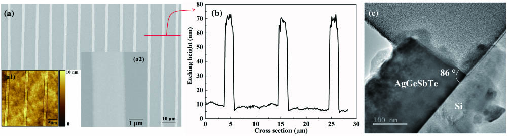
Figure 1(a) shows the SEM image of the developed AgGeSbTe film, exhibiting a clear and uniform surface morphology. Figure 1(a1) shows the AFM image of the exposed sample, presenting clear but quite shallow line structures. Figure 1(b) displays the cross-section profile of the developed film, where the exposed region is higher compared to the as-deposited region, and the height difference reaches 62 nm at the developing time of 1 min, showing a negative-tone characteristic. The magnified SEM image of Fig. 1(a2) reveals the smooth etched lines with low line edge roughness. The etching rate difference is as high as 62 nm/min, where the etching rate is defined as the ratio of etching height to time, and the etching rate difference is defined as the difference between etching rate of the exposure region and that of the non-exposed region. The high difference of etching rate means high etching selectivity of AgGeSbTe resist at
![]()
Figure 1.(a) SEM image; (a1) AFM image of the exposed sample, (a2) magnified SEM image of developed sample; (b) corresponding cross-section curve; and (c) TEM cross-section image of AgGeSbTe heat-mode resist. For (a) and (b), the laser energy is 0.7 × 10³ mJ/cm2. The gas flow ratio of CHF3/O2 is 60/2. The etching power is 200 W, and the chamber pressure is 50 mTorr with the time of 1 min. For (c), the laser energy is 1.2 × 10³ mJ/cm2, and the etching time is 3 min.
Figure 2(a) shows the influence of etching power on linewidth and etching height. It is found that the linewidth is hardly changed, while the etching height increases gradually with etching power. This is mainly due to the higher power providing more energy for active ions and making the etching rate larger. When the power reaches 240 W, the etching height increases to about 250 nm, which is nearly the same as the thickness of AgGeSbTe film. Figure 2(b) shows the influence of developing time on linewidth and etching height. It is revealed that the linewidth is hardly changed, whereas the etching height increases firstly and then reduces with the increasing developing time. When the developing time is 2 min, the etching height reaches the maximum. The reduction of height is due to the weakened etching resistance and increased etching rate of the exposed region after 3 min. Figure 2(c) depicts the influence of laser energy on linewidth and etching height, respectively. One can see the increment of linewidth and height when the laser energy becomes larger. The reason is that the generated heat becomes more and more as the laser energy increases, which enhances the thermal diffusion in the horizontal and vertical directions[
![]()
Figure 2.Dependence of (a) etching power, (b) developing time, and (c) laser power on linewidth and height of grating structures. For (a), the laser energy is 0.8 × 10³ mJ/cm2. The gas flow ratio of CHF3/O2 is 60/2, and the chamber pressure is 50 mTorr with the time of 4 min. For (b), the laser energy is 0.7 × 10³ mJ/cm2. The gas flow ratio of CHF3/O2 is 60/2, and the etching power is 200 W with the chamber pressure of 50 mTorr. For (c), the gas flow ratio of CHF3/O2 is 60/2, the etching power is 200 W, the chamber pressure is 50 mTorr, and the developing time is 3 min. The thickness of AgGeSbTe film is 250 nm.
To more clearly understand the physical mechanism where laser energy influences the linewidth and height, the thermal distribution of AgGeSbTe resist is analyzed by COMSOL software with the finite element method. It is noted that the optical and thermal parameters of GeSbTe films are utilized due to the lack of relative parameters of AgGeSbTe[
![]()
Figure 3.(a) Relationship between sheet resistance and temperature in AgGeSbTe thin film. (b) Thermal field distribution of heat-mode resist in thickness direction. (c) and (d) Temperature profiles in radius and thickness directions, respectively.
To further understand the structural evolution after laser exposure, X-ray diffraction (XRD) patterns of AgGeSbTe films are obtained in Fig. 4(a), showing the amorphous nature in the as-deposited state, while phase separation happens and crystalline phases of Ge, Sb, and AgTe occur after laser exposure. The bonding environment is also investigated by Raman and XPS spectra [Figs. 4(b) and 4(c)]. One can see from Fig. 4(b) that the as-deposited sample presents a broad Raman peak at
![]()
Figure 4.(a) XRD patterns, (b) Raman data, and (c) XPS profiles of the as-deposited and laser-exposed AgGeSbTe films, where the exposed energy is 0.7 × 10³ mJ/cm2.
In the previous research[
Etching resistance of AgGeSbTe resist is further evaluated via
![]()
Figure 5.AFM cross-section profiles of (a) development, (b) etching of AgGeSbTe resist on Si substrate, and (c) etching of the pure Si, where the exposed energy is 1.2 × 10³ mJ/cm2. For development of (a), the gas flow ratio of CHF3/O2 is 60/2. The etching power is 200 W, and the chamber pressure is 50 mTorr with the developing time of 3 min. Inset of (a) is SEM cross-section image of the developed sample. For Si etching of (b) and (c), the gas flow ratio of SF6/Ar is 15/35. The etching power is 150 W, and the chamber pressure is 50 mTorr with the etching time of 5 min.
4. Conclusion
In summary, an AgGeSbTe thin film is proposed as a negative heat-mode resist for dry lithography. It is found that the resist possesses high etching selectivity with the etching rate difference of as high as 62 nm/min. The etched sidewall is steep without the obvious lateral corrosion. The influences of laser energy, etching power, and developing time on linewidth and developing height are also investigated. The underlying physical mechanism is further analyzed. Results of XRD, Raman, and XPS profiles indicate that laser exposure induces the phase separation of AgGeSbTe resist and the occurrence of Ge, Sb, and AgTe crystals, which is the basis of etching selectivity. Besides, the AgGeSbTe resist possesses good etching resistance with the etching selectivity of Si to AgGeSbTe resist of as high as 19. The proposed AgGeSbTe resist may have potential applications in micro/nano fabrications.
References
[1] J. Wei. Laser Heat-Mode Lithography: Principle and Methods(2019).
[2] A. S. Basu, S. McNamara, Y. B. Gianchandani. Scanning thermal lithography: maskless, submicron thermochemical patterning of photoresist by ultracompliant probes. J. Vac. Sci. Technol. B, 22, 3217(2004).
[3] W. C. Tian, Y. H. Ho, C. H. Chen, C. Y. Kuo. Sensing performance of precisely ordered TiO2 nanowire gas sensors fabricated by electron-beam lithography. Sensors, 13, 865(2013).
[4] S. Wang, Z. Zhou, B. Li, C. Wang, Q. Liu. Progresses on new generation laser direct writing technique. Mater. Today Nano, 16, 100142(2021).
[5] J. Chen, G. Chen, Q. Zhan. Self-aligned fiber-based dual-beam source for STED nanolithography. Chin. Opt. Lett., 19, 072201(2021).
[6] T. Yang, H. Lin, B. Jia. Ultrafast direct laser writing of 2D materials for multifunctional photonics devices [Invited]. Chin. Opt. Lett., 18, 023601(2020).
[7] T. Jiang, S. Gao, Z. Tian, H. Zhang, L. Niu. Fabrication of diamond ultra-fine structures by femtosecond laser. Chin. Opt. Lett., 18, 101402(2020).
[8] Y. Usami, T. Watanabe, Y. Kanazawa, K. Taga, H. Kawai, K. Ichikawa. 405 nm laser thermal lithography of 40 nm pattern using super resolution organic resist material. Appl. Phys. Express, 2, 126502(2009).
[9] B. J. Zeng, J. Z. Huang, R. W. Ni, N. N. Yu, W. Wei, Y. Z. Hu, Z. Li, X. S. Miao. Metallic resist for phase-change lithography. Sci. Rep., 4, 5300(2014).
[10] T. Luo, Z. Li, Q. He, X. Miao. Pr-based metallic glass films used as resist for phase-change lithography. Opt. Express, 24, 5754(2016).
[11] H. Xi, Q. Liu, Y. Tian, Y. Wang, S. Guo, M. Chu. Ge2Sb1.5Bi0.5Te5 thin film as inorganic photoresist. Opt. Mater. Express, 2, 461(2012).
[12] H. Xi, Q. Liu, Y. Tian, S. Guo, M. Cu, G. Zhang. The study on SiO2 pattern fabrication using Ge1.5Sn0.5Sb2Te5 as resists. J. Nanosci. Nanotechnol., 13, 829(2013).
[13] Y. Meng, J. K. Behera, Z. Wang, J. Zheng, J. Wei, L. Wu, Y. Wang. Nanostructure patterning of C-Sb2Te3 by maskless thermal lithography using femtosecond laser pulses. Appl. Surf. Sci., 508, 145228(2020).
[14] J. Wei, K. Zhang, T. Wei, Y. Wang, Y. Wu, M. Xiao. High-speed maskless nanolithography with visible light based on photothermal localization. Sci. Rep., 7, 43892(2017).
[15] Z. Wang, J. Zheng, G. Chen, K. Zhang, T. Wei, Y. Wang, X. Liu, Z. Mo, T. Gao, M. Wen, J. Wei. Laser-assisted thermal exposure lithography: arbitrary feature sizes. Adv. Eng. Mater., 23, 2001468(2021).
[16] K. Zhang, Z. Wang, G. Chen, J. Zheng, Z. Mo, Y. Wang, J. Wei. Laser heat-mode patterning with improved aspect-ratio. Mat. Sci. Semicon. Proc., 134, 106018(2021).
[17] G. Chen, J. Zheng, Z. Wang, K. Zhang, Z. Mo, X. Liu, T. Gao, Y. Wang, J. Wei. Fabrication of micro/nano multifunctional patterns on optical glass through chalcogenide heat-mode resist AgInSbTe. J. Alloys Compd., 867, 158988(2021).
[18] Y. Q. Huang, R. Huang, Q. L. Liu, C. C. Zheng, J. Q. Ning, Y. Peng, Z. Y. Zhang. Realization of III-V semiconductor periodic nanostructures by laser direct writing technique. Nanoscale Res. Lett., 12, 12(2017).
[19] Z. Wang, K. Zhang, G. Chen, Z. Zhu, Y. Wang, J. Wei. A metal lift-off process through hyperbolic undercut of laser heat-mode lithography. Mater. Lett., 264, 127344(2020).
[20] T. Wei, B. Liu, W. Li, Y. Ling, J. Hu, Q. Liu, M. Cheng, J. Wei. CrSb2Te thin film as a dry resist and its etching mechanism for lithography application. Mater. Chem. Phys., 266, 124558(2021).
[21] T. Wei, J. Wei, Y. Wang, L. Zhang. Manipulation and simulations of thermal field profiles in laser heat-mode lithography. J. Appl. Phys., 122, 223107(2017).
[22] J. H. Han, K.-S. Jeong, M. Ahn, D.-H. Lim, W. J. Yang, S. Jong Park, M.-H. Cho. Modulation of phase change characteristics in Ag-incorporated Ge2Sb2Te5 owing to changes in structural distortion and bond strength. J. Mater. Chem. C, 5, 3973(2017).
[23] S. Hwang, H. Park, D. Kim, H. Lim, C. Lee, J. H. Han, Y.-K. Kwon, M.-H. Cho. Ultra-low energy phase change memory with improved thermal stability by tailoring the local structure through Ag doping. ACS Appl. Mater. Inter., 12, 37285(2020).
[24] T. Wei, Q. Wang, S. Song, Z. Song, B. Liu. Reversible phase-change characteristics and structural origin in Cr doped Ge2Sb2Te5 thin films. Thin Solid Films, 716, 138434(2020).


Set citation alerts for the article
Please enter your email address

© Copyright 2018-2021 | Chinese Laser Press. All Rights Reserved 沪ICP备15018463号-20