• Opto-Electronic Engineering
  • Vol. 50, Issue 3, 220073 (2023)
Bin Dong1, Juan Zhang2, Dawei Wang1, Yiyuan Zhang1, Leran Zhang1, Rui Li1, Chen Xin1, Shunli Liu1, Zihang Zhang1, Hao Wu1, Shaojun Jiang1, Suwan Zhu1, Bingrui Liu1、*, and Dong Wu1、**
Author Affiliations
  • 1CAS Key Laboratory of Mechanical Behavior and Design of Materials, Key Laboratory of Precision Scientific Instrumentation of Anhui Higher Education Institutes, Department of Precision Machinery and Precision Instrumentation, University of Science and Technology of China, Hefei, Anhui 230026, China
  • 2Department of Clinical Laboratory, the First Affiliated Hospital of USTC, Division of Life Sciences and Medicine, University of Science and Technology of China, Hefei, Anhui 230001, China
  • show less
    DOI: 10.12086/oee.2023.220073 Cite this Article
    Bin Dong, Juan Zhang, Dawei Wang, Yiyuan Zhang, Leran Zhang, Rui Li, Chen Xin, Shunli Liu, Zihang Zhang, Hao Wu, Shaojun Jiang, Suwan Zhu, Bingrui Liu, Dong Wu. Femtosecond laser micromachining optical devices[J]. Opto-Electronic Engineering, 2023, 50(3): 220073 Copy Citation Text show less
    Schematic diagram of the super-resolution processing principle and characteristics after processing[4]. Figure reproduced with permission from ref. [4] © Springer Nature
    Fig. 1. Schematic diagram of the super-resolution processing principle and characteristics after processing[4]. Figure reproduced with permission from ref. [4] © Springer Nature
    Femtosecond laser direct writing[45]. Figure reproduced with permission from ref. [45] © De Gruyter
    Fig. 2. Femtosecond laser direct writing[45]. Figure reproduced with permission from ref. [45] © De Gruyter
    Schematic diagram of the femtosecond laser fabrication based on diffractive optical elements and characteristics after processing[49]. Figure reproduced with permission from ref. [49] © Springer Nature
    Fig. 3. Schematic diagram of the femtosecond laser fabrication based on diffractive optical elements and characteristics after processing[49]. Figure reproduced with permission from ref. [49] © Springer Nature
    The schematic diagram of the digital micromirror projection system based on femtosecond laser two-photon polymerization and spatio-temporal focusing and characteristics after processing[57]. Figure reproduced with permission from ref. [57] © The American Association for the Advancement of Science(AAAS)
    Fig. 4. The schematic diagram of the digital micromirror projection system based on femtosecond laser two-photon polymerization and spatio-temporal focusing and characteristics after processing[57]. Figure reproduced with permission from ref. [57] © The American Association for the Advancement of Science(AAAS)
    Parallel processing based on spatial light modulator. (a) Helical scanning of femtosecond ring-shaped vortex beam based on spatial light modulator[65]; (b) Generation of Mathieu beam based on spatial light modulator[66]; (c) Fabrication of microtubes using C-shaped Bessel beam generated by spatial light modulator[68]. Figure reproduced with permission from: (a) ref. [65] © Wiley; (b) ref. [66] and (c) ref. [68] © American Chemical Society.
    Fig. 5. Parallel processing based on spatial light modulator. (a) Helical scanning of femtosecond ring-shaped vortex beam based on spatial light modulator[65]; (b) Generation of Mathieu beam based on spatial light modulator[66]; (c) Fabrication of microtubes using C-shaped Bessel beam generated by spatial light modulator[68]. Figure reproduced with permission from: (a) ref. [65] © Wiley; (b) ref. [66] and (c) ref. [68] © American Chemical Society.
    Focal field engineering based on spatial light modulator[72]. Figure reproduced with permission from ref. [72] © John Wiley and Sons
    Fig. 6. Focal field engineering based on spatial light modulator[72]. Figure reproduced with permission from ref. [72] © John Wiley and Sons
    Schematic diagram of the femtosecond (fs) laser interference processing and characteristics after processing[79]. Figure reproduced with permission from ref. [79] © MDPI
    Fig. 7. Schematic diagram of the femtosecond (fs) laser interference processing and characteristics after processing[79]. Figure reproduced with permission from ref. [79] © MDPI
    Processing of microlenses. (a) Transferring[83]; (b) Wet etching[84]; (c) Dry etching[86]. Figure reproduced with permission from: (a) ref. [83], (b) ref. [84] and (c) ref. [86] © Wiley
    Fig. 8. Processing of microlenses. (a) Transferring[83]; (b) Wet etching[84]; (c) Dry etching[86]. Figure reproduced with permission from: (a) ref. [83], (b) ref. [84] and (c) ref. [86] © Wiley
    Micromachining of microlenses based on two-photon polymerization of femtosecond laser. (a) Protein-based microlens in response to the change of pH[93]; (b) Double-material compound eye in response to the change of pH[25]. Figure reproduced with permission from: (a) ref. [93] and (b) ref. [25] © Wiley
    Fig. 9. Micromachining of microlenses based on two-photon polymerization of femtosecond laser. (a) Protein-based microlens in response to the change of pH[93]; (b) Double-material compound eye in response to the change of pH[25]. Figure reproduced with permission from: (a) ref. [93] and (b) ref. [25] © Wiley
    Innovative microlenses. (a) Complex microlens arrays based on laser-induced thermal deformation[95]; (b) Direct patterning of polymeric microlenses based on the combination of femtosecond laser and surface tension of droplet[96]; (c) Integration of compound lens on the surface of CMOS image sensor based on femtosecond laser[82]. Figure reproduced with permission from: (a) ref.[95] © Springer Nature; (b) ref. [96] © American Chemical Society; (c) ref. [82] © The American Association for the Advancement of Science (AAAS)
    Fig. 10. Innovative microlenses. (a) Complex microlens arrays based on laser-induced thermal deformation[95]; (b) Direct patterning of polymeric microlenses based on the combination of femtosecond laser and surface tension of droplet[96]; (c) Integration of compound lens on the surface of CMOS image sensor based on femtosecond laser[82]. Figure reproduced with permission from: (a) ref.[95] © Springer Nature; (b) ref. [96] © American Chemical Society; (c) ref. [82] © The American Association for the Advancement of Science (AAAS)
    Femtosecond laser direct writing optical waveguide. (a) Single-line waveguide[100]; (b) Double-line waveguide[106]; (c) Depressed cladding waveguide[111]. Figure reproduced with permission from: (a) ref. [100] and (c) ref. [111] © Wiley; (b) ref. [106] © MDPI.
    Fig. 11. Femtosecond laser direct writing optical waveguide. (a) Single-line waveguide[100]; (b) Double-line waveguide[106]; (c) Depressed cladding waveguide[111]. Figure reproduced with permission from: (a) ref. [100] and (c) ref. [111] © Wiley; (b) ref. [106] © MDPI.
    Fabrication of micro-gratings based on femtosecond laser. (a) Procedures of femtosecond laser fabricating FBG[117]; (b) Fabrication of LIPSS on Si substrate utilizing cylindrical lens based on femt osecond laser[129]; (c) Fabrication of continuous phase vortex grating based on two-photon polymerization of femtosecond laser[22]. Figure reproduced with permission from: (a) ref. [117] © American Chemical Society; (b) ref. [129] © Wiley; (c) ref. [22] © AIP Publishing
    Fig. 12. Fabrication of micro-gratings based on femtosecond laser. (a) Procedures of femtosecond laser fabricating FBG[117]; (b) Fabrication of LIPSS on Si substrate utilizing cylindrical lens based on femt osecond laser[129]; (c) Fabrication of continuous phase vortex grating based on two-photon polymerization of femtosecond laser[22]. Figure reproduced with permission from: (a) ref. [117] © American Chemical Society; (b) ref. [129] © Wiley; (c) ref. [22] © AIP Publishing
    Fabrication of woodpile photonic crystal whose stop band lies in the visible spectrum based on femtosecond laser[146]. Figure reproduced with permission from ref. [146] © Springer Nature
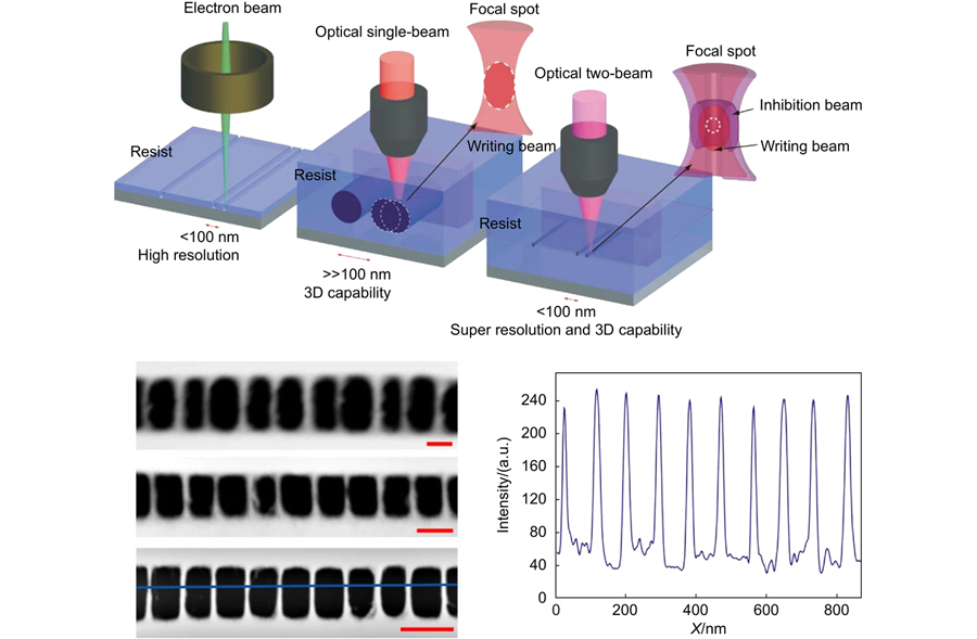
    Fig. 13. Fabrication of woodpile photonic crystal whose stop band lies in the visible spectrum based on femtosecond laser[146]. Figure reproduced with permission from ref. [146] © Springer Nature
    Fabrication of nonlinear photonic crystal based on femtosecond laser. (a) Fabrication of nonlinear photonic crystal in LiNbO3[150]; (b) Fabrication of nonlinear photonic crystal in BCT[151]. Figure reproduced with permission from: (a) ref. [150] and (b) ref. [151] © Springer Nature
    Fig. 14. Fabrication of nonlinear photonic crystal based on femtosecond laser. (a) Fabrication of nonlinear photonic crystal in LiNbO3[150]; (b) Fabrication of nonlinear photonic crystal in BCT[151]. Figure reproduced with permission from: (a) ref. [150] and (b) ref. [151] © Springer Nature
    Bin Dong, Juan Zhang, Dawei Wang, Yiyuan Zhang, Leran Zhang, Rui Li, Chen Xin, Shunli Liu, Zihang Zhang, Hao Wu, Shaojun Jiang, Suwan Zhu, Bingrui Liu, Dong Wu. Femtosecond laser micromachining optical devices[J]. Opto-Electronic Engineering, 2023, 50(3): 220073
    Download Citation