
Pengchang Yang, Jinchuan Zhang, Zenghui Gu, Chuanwei Liu, Yue Zhao, Fengmin Cheng, Shenqiang Zhai, Ning Zhuo, Junqi Liu, Lijun Wang, Shuman Liu, Fengqi Liu. Coupled-ridge waveguide quantum cascade laser array lasing at λ ~ 5 µm[J]. Journal of Semiconductors, 2021, 42(9): 092901
- Journal of Semiconductors
- Vol. 42, Issue 9, 092901 (2021)
Abstract
1. Introduction
Quantum cascade lasers (QCLs) have been intensely researched in recent years for narrow line-width and high power mid-infrared (MIR) emissions excited by the desperate need of applications, for instance remote gas-sensing, free-space optical communication and high-resolution spectroscopy[
In this paper, we demonstrated high peak power substrate-emitting DFB QCL arrays lasing at λ ~ 5 µm by employing an optimized CRW structure. Five-element QCL arrays were simulated and fabricated through a two-step etching method to extend the CRW structure to a mid-infrared. By introducing a buried 2nd-order DFB grating, the devices could work at a stable single longitudinal mode with a linear tuning coefficient of –0.2 cm–1/K. Lateral far-field with the main peak near the diffraction-limited intensity curve of about 10.7° was observed in a ridge-width direction even at full power. The peak output power from the substrate surpassed 1 W at 25 °C. The main-lobed far-field distribution and high output power of these devices make them very essential in real applications.
2. Simulation and fabrication
A double-phonon resonant design was introduced into the active region of this device with an emitting wavelength of 5 µm. The whole wafer was co-grown by solid-source molecular beam epitaxy (MBE) and metal organic vapor phase epitaxy (MOVPE) on an n-InP substrate (Si, 2 × 1017 cm–3). The active region and InGaAs confined layers were grown by MBE and the InP cladding was grown by MOVPE. Along the epitaxial layers sequence, the InP bottom cladding layer (5 µm, Si, 2.2 × 1016 cm–3), InGaAs confined layer (300 nm, Si, 2 × 1016 cm–3), active region (40-stages In0.6Ga0.4As/In0.4Al0.6As superlattice with a strain-compensated design and a total thickness of ~2 µm), InGaAs confined layer (300 nm, Si, 2 × 1016 cm–3), InP upper cladding layer (3 µm, Si, 2.2 × 1016 cm–3), InP gradually doped layer (250 nm, Si, 2 × 10¹⁷ to 5 × 1017 cm–3) and InP highly doped contact layer (500 nm, Si, 5.5 × 1018 cm–3) was grown respectively.
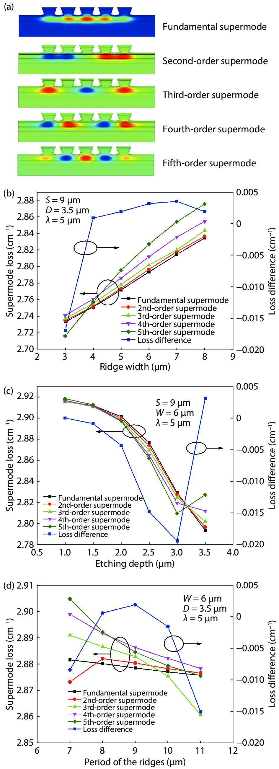
Before fabrication, simulation was conducted with COMSOL to select the optimal parameters of the CRW structure. Based on our earlier research, the mode selection of the array was mainly related to the modal waveguide loss[
![]()
Figure 1.(Color online) (a) The near-field distribution of the fundamental supermode and high-order supermode. (b) The dependence of loss difference of the modal waveguide between the high-order and fundamental supermode on ridge width with a fixed etching depth at 3.5
where S is the period of the ridges,
Before the top cladding layer was grown, a buried 2nd-order grating (period Ʌ = 1.58 µm, duty cycle σ = 0.4, and depth d ~ 180 nm) was patterned and transformed on the InGaAs upper constrain layer by using holographic lithography and wet etching technique, as is shown in Fig. 2(a). Then the wafer was etched into a five-element CRW structure through standard photolithography techniques and reactive ion etching (RIE). The etching depth was about 2.8 µm and the top ridge width was 7 µm. This was the first etching step and a good etching profile was ensured by the excellent isotropy of RIE. After that, a wet chemical etching process was used to enlarge the etching depth. Then an inverted conical geometric structure can be obtained, where there is a larger index contrast between the etched and un-etched regions. A total etching depth of 3.5 µm was obtained, which means that we protected the integrity of the active region. Due to the isotropy of the wet etching, the top ridge width was decreased from 7 to 6 µm. The interelement space between two adjacent ridges was 3 µm. The cross-section image of the five-element device was shown as Fig. 2(b). Through this two-step etching method, the loss difference was increased considerably and the coupling strength among array elements was enhanced for mid-wave infrared QCL arrays.
![]()
Figure 2.(Color online) (a) The image of the buried grating from SEM. (b) The cross-section photography of the device. (c) A 3-D sketch of the structure.
After completing the etching process, a SiO2 insulating layer with a 450 nm thickness was deposited by plasma-enhanced chemical vapor deposition (PECVD) around the ridges. We set a 3 µm wide window for electron injection on each ridge by photolithography and wet etching and ohmic contact was provided by a Ti/Au layer. To further enhance the heat dissipation, an additional 4 µm thick gold layer was electroplated. Then we deposited a Ge/Au/Ni/Au metal contact layer on the backside of the sample after thinning the substrate down to 150 µm. And then a 160 µm wide substrate-emitting window was patterned by chemical etching. Finally, the sample was high-reflectivity (HR) coated with Al2O3/Ti/Au/Al2O3 (200/10/100/120 nm) on the back facets by e-beam evaporation, and then cleaved into 2 mm long devices for testing. The QCL arrays were bonded epi-layers down to a copper heatsink with an indium solder.
3. Results and discussion
The far-field pattern of the laser arrays in the ridge-width direction was most concerned. QCL arrays’ far-field measurements were carried out on a step-motor controlled rotation stage with a thermal resistor and a thermo-electrical cooler (TEC) monitoring and regulating the heatsink temperature. The devices were operated under a pulsed mode at 25 °C with a repeat frequency of 10 kHz and a pulse width of 1 µs. The mid-infrared emission was collected by a room-temperature HgCdTe detector (Viggo, PVMI-8) with a distance of 40 cm away from the substrate-emitting window of the laser array. For the substrate emitting device, a main-lobed far-field distribution with a divergence angle of 10° was observed in the ridge-width direction at 2 A, as shown in Fig. 3(a). The full width at half maximum (FWHM) of the far-field main-lobes were about 1.5 times the diffraction limit (D.L.) near the threshold. The devices did not operate in single-spatial mode causing the nearest-neighbor coupling to be inevitable due to a very low loss differential. In addition, the inevitable nearest-neighbor coupling may lead to other modes and different modes have different thresholds. Then, while the current increased from the threshold, other modes occurred, the far-field would widen and other peak intensities become obvious. But even at a high current of 7 A, the devices still kept the main-lobed far-field distribution with a divergence angle of 10.7°. The phenomenon can be concluded from the same equation:
![]()
Figure 3.(Color online) (a) The devices’ far-field distribution from the substrate emitting windows in the ridge-width direction at different operating current. (b) The far-field distribution from the substrate emitting windows of the QCL array in the cavity direction at the current of 6 A.
where
The power–current characteristics of the laser arrays are shown in Fig. 4. The test was carried out at room temperature of 25 °C in the pulsed mode with a repeated frequency of 10 kHz and pulse width of 500 ns. The emitted light power was measured by a calibrated thermopile detector (Coherent, EMP1000) placed directly ahead of the device. For the five-element device, the threshold current was about 2 A and the corresponding threshold current intensity was about 2 kA/cm2. A peak power of more than 1 W was obtained from the substrate with a slope efficiency of 0.3 W/A. The peak power emitted from the edge was about 3.4 W. The ratio of substrate-emitted power and edge-emitted power was about 31%.
![]()
Figure 4.(Color online) The power–current characteristics of the device at 25 °C. The red line and blue line represent the output power from the edge and the substrate, respectively.
The spectra of the QCL arrays were measured by a Fourier transform infrared (FTIR) spectrometer in a fast scan mode with a resolution of 0.25 cm–1. The temperature of the heatsink was stabilized with a thermo-electrical cooler (TEC). The emitting spectra of the device are shown in Fig. 5. Steady single-mode emission was observed and the lasing wavelength could be tuned continuously. The spectra were measured at different temperatures of the heatsink from 10 to 60 °C with a step of 5 °C, covering a total tuning range of 9.9 cm–1. The inset of Fig. 5 shows the dependence of the lasing frequency on the temperature of the heatsink. A linear tuning coefficient of –0.2 cm–1/K was deduced. The wide tuning range and linear tuning ability make these devices very promising in spectroscopy applications.
![]()
Figure 5.(Color online) The emitting spectra of the QCL array at different temperatures of the heatsink. The inset shows the dependence of wavelength on heatsink temperature.
4. Conclusion
We have demonstrated high-power single longitudinal mode substrate-emitting QCL arrays lasing at λ ~ 5 µm by employing a CRW structure and buried 2nd-order DFB grating. Five-element QCL arrays were simulated and fabricated to explore the coherent capability of the CRW structure. Stable main-lobed far-field distribution in the ridge-width direction with a divergence angle of 10.7° was observed even at full power. The peak output power surpassed 1 W at room temperature of 25 °C. The devices could work at a stable single longitudinal mode and could be tuned continuously with a linear temperature tuning coefficient of –0.2 cm–1/K.
Acknowledgements
This work was supported by National Basic Research Program of China (Grant Nos. 2018YFA0209103, 2018YFB2200504), in part by National Natural Science Foundation of China (Grant Nos. 61991430, 61774146, 61790583, 61734006, 61835011, 61674144, 61774150, 61805168), in part by Beijing Municipal Science & Technology Commission (Grant No. Z201100004020006), and in part by the Key projects of the Chinese Academy of Sciences (Grant No. 2018147, Grant No. YJKYYQ20190002, Grant No. QYZDJ-SSW-JSC027, Grant No. XDB43000000, Grant No. ZDKYYQ20200006). The authors would appreciate P. Liang and Y. Hu for their help in the device fabrication processing.
References
[1] Y Bai, S Tsao, N Bandyopadhyay et al. High power, continuous wave, quantum cascade ring laser. Appl Phys Lett, 99, 261104(2011).
[2] R Centeno, D Marchenko, J Mandon et al. High power, widely tunable, mode-hop free, continuous wave external cavity quantum cascade laser for multi-species trace gas detection. Appl Phys Lett, 105, 261907(2014).
[3] S Slivken, S Sengupta, M Razeghi. High power continuous operation of a widely tunable quantum cascade laser with an integrated amplifier. Appl Phys Lett, 107, 251101(2015).
[4] Y Bai, S Slivken, S R Darvish et al. High power broad area quantum cascade lasers. Appl Phys Lett, 95, 221104(2009).
[5] Y Bai, S R Darvish, S Slivken et al. Electrically pumped photonic crystal distributed feedback quantum cascade lasers. Appl Phys Lett, 91, 141123(2007).
[6] Q Y Lu, W H Guo, W Zhang et al. Room temperature operation of photonic-crystal distributed-feedback quantum cascade lasers with single longitudinal and lateral mode performance. Appl Phys Lett, 96, 051112(2010).
[7] S Menzel, L Diehl, C Pflügl et al. Quantum cascade laser master-oscillator power-amplifier with 15 W output power at 300 K. Opt Express, 19, 16229(2011).
[8] Y Bai, S Slivken, Q Y Lu et al. Angled cavity broad area quantum cascade lasers. Appl Phys Lett, 101, 081106(2012).
[9] J D Kirch, C C Chang, C Boyle et al. 5.5 W near-diffraction-limited power from resonant leaky-wave coupled phase-locked arrays of quantum cascade lasers. Appl Phys Lett, 106, 061113(2015).
[10] L Wang, J C Zhang, Z W Jia et al. Phase-locked array of quantum cascade lasers with an integrated Talbot cavity. Opt Express, 24, 30275(2016).
[11] B Meng, B Qiang, E Rodriguez et al. Coherent emission from integrated Talbot-cavity quantum cascade lasers. Opt Express, 25, 3077(2017).
[12] A Lyakh, R Maulini, A Tsekoun et al. Continuous wave operation of buried heterostructure 4.6
[13] L K Hoffmann, C A Hurni, S Schartner et al. Wavelength dependent phase locking in quantum cascade laser Y-junctions. Appl Phys Lett, 92, 061110(2008).
[14] L K Hoffmann, M Klinkmüller, E Mujagić et al. Tree array quantum cascade laser. Opt Express, 17, 649(2009).
[15] Y H Liu, J C Zhang, F L Yan et al. Coupled ridge waveguide distributed feedback quantum cascade laser arrays. Appl Phys Lett, 106, 142104(2015).
[16] C W Liu, J C Zhang, Z W Jia et al. Coupled ridge waveguide substrate-emitting DFB quantum cascade laser arrays. IEEE Photonics Technol Lett, 29, 213(2017).
[17] D Y Yao, J C Zhang, F Q Liu et al. Surface emitting quantum cascade lasers operating in continuous-wave mode above 70 °C at λ ~ 4.6

Set citation alerts for the article
Please enter your email address
© Copyright 2018-2021 | Chinese Laser Press. All Rights Reserved 沪ICP备15018463号-20