• Photonics Research
  • Vol. 5, Issue 5, 527 (2017)
Hailong Wang, Yuyang Wang, Yi Wang, Weiqing Xu, and Shuping Xu*
Author Affiliations
  • State Key Laboratory of Supramolecular Structure and Materials, Institute of Theoretical Chemistry, Jilin University, Changchun 130012, China
  • show less
    DOI: 10.1364/PRJ.5.000527 Cite this Article Set citation alerts
    Hailong Wang, Yuyang Wang, Yi Wang, Weiqing Xu, Shuping Xu. Modulation of hot regions in waveguide-based evanescent-field-coupled localized surface plasmons for plasmon-enhanced spectroscopy[J]. Photonics Research, 2017, 5(5): 527 Copy Citation Text show less
    (a) Schematic diagram of the WEF-LSP configuration. EM distributions in the waveguide layer and adjacent air layer under (b) TM and (c) TE light. Arrows disclose the polarization directions in the waveguide layers. The thickness of the waveguide is 560 nm. (d) Plots of the electric intensities along the z coordinate away from the prism. Different penetration depths of the electric field in air were observed for the TE and TM modes.
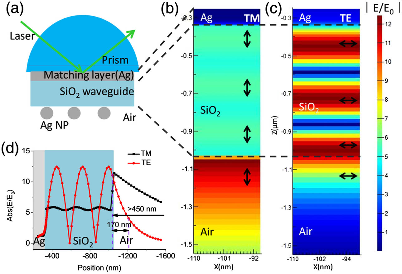
    Fig. 1. (a) Schematic diagram of the WEF-LSP configuration. EM distributions in the waveguide layer and adjacent air layer under (b) TM and (c) TE light. Arrows disclose the polarization directions in the waveguide layers. The thickness of the waveguide is 560 nm. (d) Plots of the electric intensities along the z coordinate away from the prism. Different penetration depths of the electric field in air were observed for the TE and TM modes.
    Polarizations in different surface electric fields in the present WEF configuration. Solid arrows indicate the light propagation directions and dashed arrows stand for the electric field direction in different dielectric layers. TM and TE correspond to the incident polarization to excite the waveguide modes in dielectric layer 2. The solid and dashed arrows in the “TM” and “TE” columns correspond to the propagation direction of the EM wave and vibration direction of the electric field, respectively. A circle with a dot indicates an arrow pointing to the outward page plane.
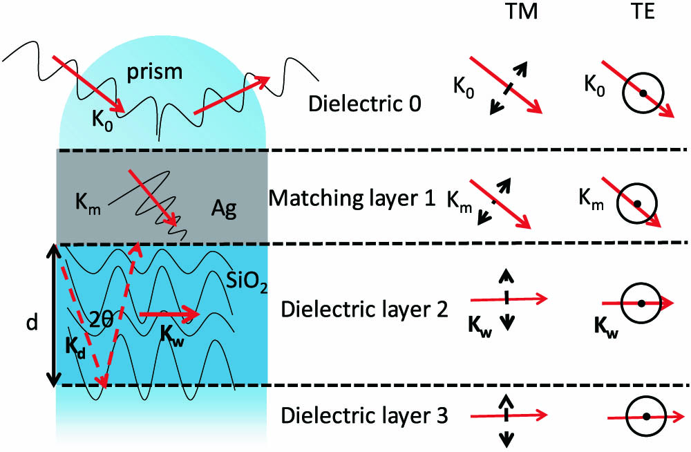
    Fig. 2. Polarizations in different surface electric fields in the present WEF configuration. Solid arrows indicate the light propagation directions and dashed arrows stand for the electric field direction in different dielectric layers. TM and TE correspond to the incident polarization to excite the waveguide modes in dielectric layer 2. The solid and dashed arrows in the “TM” and “TE” columns correspond to the propagation direction of the EM wave and vibration direction of the electric field, respectively. A circle with a dot indicates an arrow pointing to the outward page plane.
    Plots of the angle-resolved reflection spectra using a bright lamp as a light source under TM and TE polarizations, collected from the prism side by a self-built, angle-scanned spectroscopic system. Color scales in (a) and (b) indicate reflectivity, while dark color means the waveguide mode caused low reflectivity, that is, strong absorption. (c) Angle-dependent mirror reflection curves with 532 nm laser irradiation under TM and TE. For comparison, the SPR curve from a 45 nm Ag film on the Kretschmann prism is also collected.
    Fig. 3. Plots of the angle-resolved reflection spectra using a bright lamp as a light source under TM and TE polarizations, collected from the prism side by a self-built, angle-scanned spectroscopic system. Color scales in (a) and (b) indicate reflectivity, while dark color means the waveguide mode caused low reflectivity, that is, strong absorption. (c) Angle-dependent mirror reflection curves with 532 nm laser irradiation under TM and TE. For comparison, the SPR curve from a 45 nm Ag film on the Kretschmann prism is also collected.
    Measured waveguide resonance curves detected with different Ag film thicknesses as the matching layer. The 532 nm TE wave was used and the waveguide thickness was 550 nm.
    Fig. 4. Measured waveguide resonance curves detected with different Ag film thicknesses as the matching layer. The 532 nm TE wave was used and the waveguide thickness was 550 nm.
    EM distributions in the waveguide layer and Ag NPs excited by the WEF (1) with the incident polarizations of (a), (b) TE and (c), (d) TM. In contrast, the EM distributions in the waveguide layer and Ag NPs directly excited by the incident polarizations (2) of (e), (f) TE and (g), (h) TM from the air. The color bar is the linear intensity of the |E/E0|. Arrows in white are the electric polarizations at different positions. The incident angle for the direct excitation method is 60°. Waveguide is noted as “WG”.
    Fig. 5. EM distributions in the waveguide layer and Ag NPs excited by the WEF (1) with the incident polarizations of (a), (b) TE and (c), (d) TM. In contrast, the EM distributions in the waveguide layer and Ag NPs directly excited by the incident polarizations (2) of (e), (f) TE and (g), (h) TM from the air. The color bar is the linear intensity of the |E/E0|. Arrows in white are the electric polarizations at different positions. The incident angle for the direct excitation method is 60°. Waveguide is noted as “WG”.
    Top: AFM images and height plots of Ag nanospheres over the waveguide surface. The size of the left image is 10 μm×10 μm and that of the middle image is 2 μm×2 μm. Curves in the right image show the heights of the label nanospheres in the middle image. Down: (a) Reflection spectra of the WEF-LSP configuration excited by TE and TM laser. The laser wavelength is 532 nm. The reflection spectra clearly show the waveguide modes excited by TE and TM waves. (b) and (c) Corresponding SERS spectra of 4-MPY assembled on the NPs excited by the waveguide resonant modes. The excitation power for the laser is 68 mW and integration time is 30 s.
    Fig. 6. Top: AFM images and height plots of Ag nanospheres over the waveguide surface. The size of the left image is 10  μm×10  μm and that of the middle image is 2  μm×2  μm. Curves in the right image show the heights of the label nanospheres in the middle image. Down: (a) Reflection spectra of the WEF-LSP configuration excited by TE and TM laser. The laser wavelength is 532 nm. The reflection spectra clearly show the waveguide modes excited by TE and TM waves. (b) and (c) Corresponding SERS spectra of 4-MPY assembled on the NPs excited by the waveguide resonant modes. The excitation power for the laser is 68 mW and integration time is 30 s.
    (a) Fabrication of the Ag nano-hemisphere array over the waveguide surface using vacuum deposition of Ag with a through-hole UTAM as a mask. (b) AFM image of the anodic aluminum oxide template to fabricate the Ag hemisphere array. (c) and (d) SEM images of the prepared Ag hemisphere array. The scale bar is 10 μm in (c) and 1 μm in (d). (e) AFM height mapping of the Ag nano-hemisphere array. (f) Waveguide modes with Ag nano-hemispheres excited by TE and TM waves and the corresponding SERS spectra of 4-MPY under the waveguide resonant modes (g) and (h). The excitation power for the laser is 68 mW and integration time is 30 s. (i) EM field distribution of the Ag hemisphere under WEF coupling under TM and TE polarizations. The scale bar of the electric field is linear.
    Fig. 7. (a) Fabrication of the Ag nano-hemisphere array over the waveguide surface using vacuum deposition of Ag with a through-hole UTAM as a mask. (b) AFM image of the anodic aluminum oxide template to fabricate the Ag hemisphere array. (c) and (d) SEM images of the prepared Ag hemisphere array. The scale bar is 10 μm in (c) and 1 μm in (d). (e) AFM height mapping of the Ag nano-hemisphere array. (f) Waveguide modes with Ag nano-hemispheres excited by TE and TM waves and the corresponding SERS spectra of 4-MPY under the waveguide resonant modes (g) and (h). The excitation power for the laser is 68 mW and integration time is 30 s. (i) EM field distribution of the Ag hemisphere under WEF coupling under TM and TE polarizations. The scale bar of the electric field is linear.
    Hailong Wang, Yuyang Wang, Yi Wang, Weiqing Xu, Shuping Xu. Modulation of hot regions in waveguide-based evanescent-field-coupled localized surface plasmons for plasmon-enhanced spectroscopy[J]. Photonics Research, 2017, 5(5): 527
    Download Citation