Hailong Wang, Yuyang Wang, Yi Wang, Weiqing Xu, Shuping Xu. Modulation of hot regions in waveguide-based evanescent-field-coupled localized surface plasmons for plasmon-enhanced spectroscopy[J]. Photonics Research, 2017, 5(5): 527
Copy Citation Text
Coupling efficiency between the localized surface plasmons (LSPs) of metal nanoparticles (NPs) and incident light dominates the sensitivities of plasmon-based sensing spectroscopies and imaging techniques, e.g., surface-enhanced Raman scattering (SERS) spectroscopy. Many endogenous features of metal NPs (e.g., size, shape, aggregation form, etc.) that have strong impacts on their LSPs have been discussed in detail in previous studies. Here, the polarization-tuned electromagnetic (EM) field that facilitates the LSP coupling is fully discussed. Numerical analyses on waveguide-based evanescent fields (WEFs) coupled with the LSPs of dispersed silver nanospheres and silver nano-hemispheres are presented and the applicability of the WEF-LSPs to plasmon-enhanced spectroscopy is discussed. Compared with LSPs under direct light excitation that only provide 3–4 times enhancement of the incidence field, the WEF-LSPs can amplify the electric field intensity about 30–90 times (equaling the enhancement factor of 106–108 in SERS intensity), which is comparable to the EM amplification of the SERS “hot spot” effect. Importantly, the strongest region of EM enhancement around silver nanospheres can be modulated from the gap region to the side surface simply by switching the incident polarization from TM to TE, which widely extends its sensing applications in surface analysis of monolayer of molecule and macromolecule detections. This technique provides us a unique way to achieve remarkable signal gains in many plasmon-enhanced spectroscopic systems in which LSPs are involved.
Plasmonics is a rapidly developing branch in nanophotonics that embodies the features of the collective electron excitations in noble metal films and nanoparticles (NPs). The localized surface plasmon resonance (LSPR) effect on silver and gold NPs induces strong electric field of 100–10,000 times of the incidence field near the particle surface, and has been widely used for various sensing and spectroscopy applications [1,2]. As signal-enhancement media, metal NPs have been frequently used in a great number of surface-enhanced Raman scattering (SERS) and plasmon-based sensing methods due to their high enhancement activity, very low cost, easy preparation, and surface modification [3,4]. The high-efficiency local coupling of localized surface plasmons (LSPs) plays a key role and needs diversified solutions. Most attempts have focused in depth on the optimization of size, shape, aggregation, and materials of the metal NPs [1,2,5–7], which can not only increase the extinction cross-section of metal NPs to achieve the largest local electric field but also bring about a “lightning rod” effect due to geometric features and “hot spot” effect due to the formation of nanoscale gaps. However, neither the “lightning rods” nor the “hot spots” are freely used in SERS detections because these configurations require accurate nanoscale manipulation, and the “hot” regions are very limited in both number and space [8]. Moreover, the hot regions are usually in ultra-narrow gaps where the probed molecules are hard to access. Therefore, efforts have been made to extend “gap” to “surface” and achieve relatively larger, programmed areas that allow for the adsorption of large molecules [9].
As we know, the two-fold enhancement mechanism is widely used for explaining the plasmon-enhanced spectroscopy, e.g., SERS, in which the incident light in the far field is captured to the near field by a metal NP, and then Raman photons coupled with metal plasmons in the near field are scattered heavily through the same NP to the far field [10]. Thus, two feasible ways to achieve higher signal gain are fully considered: (1) amplifying the incident light field on metal NPs, and (2) collecting the scattering signal as much as possible through the optimization of the light path of the measurement setups, as well as SERS substrate designs, e.g., using Yagi–Uda antennas [11]. However, the LSPR-based nanoantenna brings a fusiform radiation pattern, which causes low collection efficiency when using an objective lens with a numerical aperture less than 1 [12]. Therefore, amplifying the incident light field by the focusing optical elements to promote the coupling process of LSPs is the main strategy in LSPR-based spectroscopy and sensing. In recent studies, waveguide-based configurations are utilized to couple LSPs for the excitation of Raman photons, which is one practical way to amplify the LSPs by the waveguide resonance [13–19]. These insightful studies lead us to believe that the waveguide-based evanescent field (WEF) excitation may be a unique way to couple LSPs that is superior to direct, focused laser irradiation due to higher harvesting efficiency for the incident light.
In this paper, we demonstrate an evanescent-field-based waveguide mode to couple the LSPs of the Ag nanospheres and hemispheres for SERS enhancement. The distributions of the local electromagnetic (EM) field around the Ag NPs can be modulated by the incident light with different polarizations. This WEF-LSP configuration can amplify the local EM field 30–90 times, that is, dozens-fold the EM field produced by the individual LSPs. The polarization dependence and EM enhancement of the LSPs were evidenced by the SERS signal of the probe molecules adjacent to the local fields. This study provides a valuable strategy to amplify incident the light field, which can be combined with shell-isolated nanoparticle-enhanced Raman spectroscopy (SHINERS) [20] and other plasmon-related techniques where LSPs are involved.
Sign up for Photonics Research TOC. Get the latest issue of Photonics Research delivered right to you!Sign up now
2. EXPERIMENTAL SECTION
A. Preparation of Waveguide Structure
Figure 1(a) shows the WEF configuration. A silica planar waveguide was prepared on a flat glass slide (BK7, as same as the prism with the refractive index at 532 nm, ), while a thin Ag film as a matching layer exists between the glass slide and the waveguide layer. The silver film was prepared by vacuum evaporation deposition on the glass slide with an evaporation speed of 0.1–0.2 nm/s (Beijing Technol. Sci. Co. Ltd., China), and its thickness was optimized at 35 nm, which refers to a measured thickness by the surface profiler (Dektak 150, Veeco Co.). Next, a silica waveguide layer ( at 532 nm) was fabricated over the Ag film with thickness of 560 nm by means of plasma-enhanced chemical vapor deposition (Oxford Plasmalab System 100 PECVD) method. The glass slide with the prepared waveguide was attached to the bottom surface of a semicylindrical prism (BK7, at 532 nm) via a refractive index matching oil (, Shanghai Specimen and Model Factory).
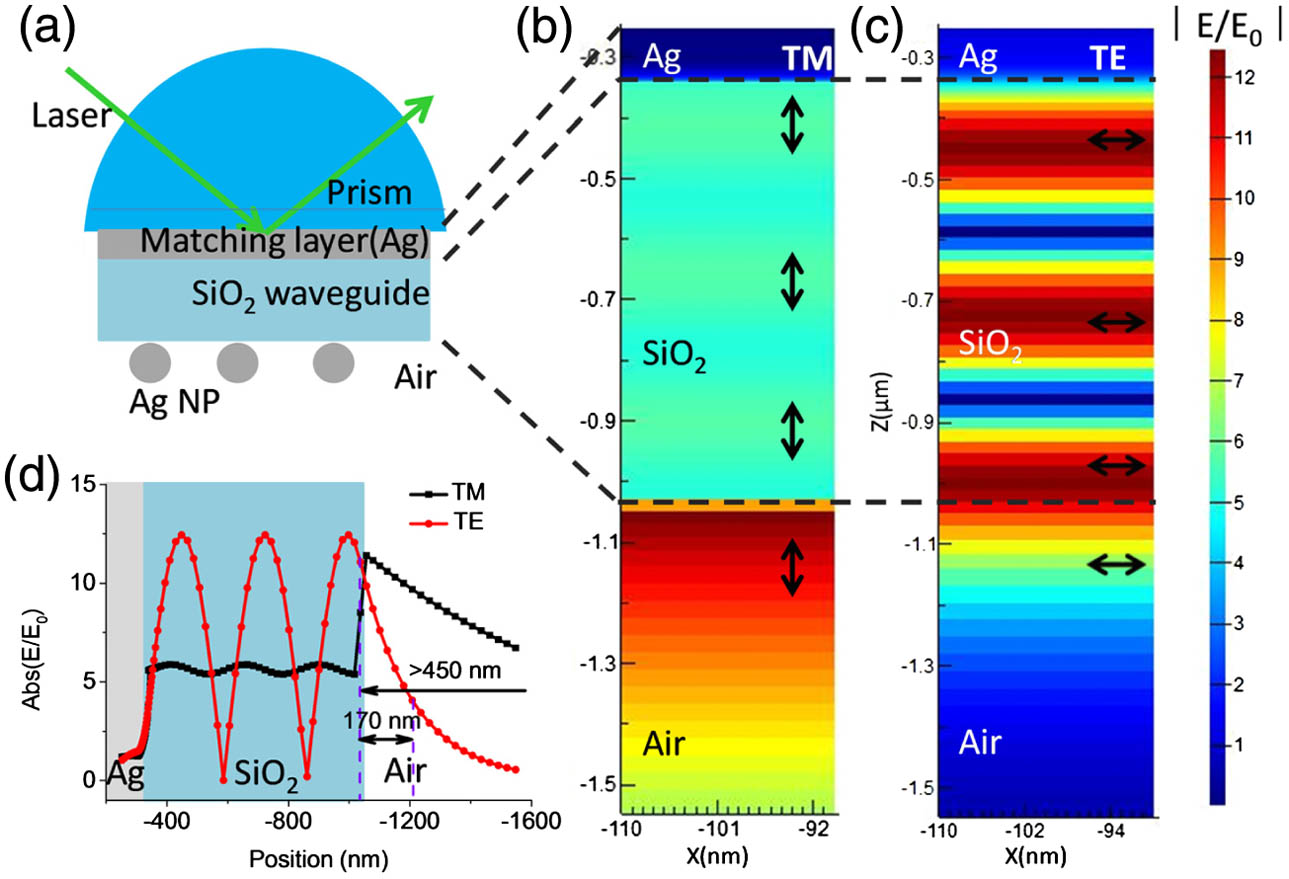
Figure 1.(a) Schematic diagram of the WEF-LSP configuration. EM distributions in the waveguide layer and adjacent air layer under (b) TM and (c) TE light. Arrows disclose the polarization directions in the waveguide layers. The thickness of the waveguide is 560 nm. (d) Plots of the electric intensities along the coordinate away from the prism. Different penetration depths of the electric field in air were observed for the TE and TM modes.
On the waveguide, we first deposited tiny Ag islands (the deposition thickness is supposed to equal 3 nm) to facilitate the loading of linking molecules (4-mercaptopyridine, 4-MPY). Next, the waveguide slide was immersed in a 4-MPY (Acros Organics Chemical Co.) ethanol solution () for 30 min and then cleaned with ethanol and dried. Thus, 4-MPY was fixed on the waveguide with its mercapto group forming an -Ag bond. Then the slide was immersed in the Ag colloid solution for 12 h for the Ag NP assembly with the N atom end of 4-MPY. Ag colloid with a size of was synthesized according to Lee’s method [2]. The waveguide with Ag NPs was characterized by scanning electron microscopy (SEM, JEOL JSM-6700F) and atomic force microscopy (AFM).
Another WEF-LSP configuration is designed by the Ag nano-hemisphere array, which is prepared by depositing Ag on a glass slide with an anodized aluminum oxide (AAO) as a mask. The preparation of an AAO has been reported in previous publications in a two-step method [21,22]. First, high-purity (99.999%) aluminum sheets (Cuibolin) cut into were annealed under 500°C in ambience and then cleaned in acetone for degreasing. The clean aluminum sheets were electro-polished in a mixed solution of and ethanol (volume ratio 2:5), creating mirror-like surfaces on the aluminum. The polishing of the aluminum sheets was performed in a simple self-made electrochemical cell composed of a circulation water system to cool down the electrolyte, a DC power supply, and a counterelectrode made of titanium. According to a previous study [23,24], the voltage to fabricate an AAO on an Al sheet is based on the empirical voltage of the 2.5 nm/V rule. The first oxidation was carried out under 40 V in 0.3 mol/L oxalic solution at a temperature of 4°C for 12 h. The oxidized layer was then removed by an etching solution for leaving pits on the aluminum sheet. The second oxidation was 2 min at the voltage of 40 V in 0.3 mol/L oxalic solution, and about a 200 nm oxidized layer would be achieved.
To use AAO as a mask, the barrier layer of the AAO and the Al base should be effectively removed uniformly. Since the AAO is very thin and frail, we fabricated a polymer supporting layer on the AAO surface by spin-coating (SIYOUYEN Electronic Technology Co., Ltd. Shanghai) a 2% poly(methyl methacrylate) (PMMA) over the AAO and drying it in an oven. Then the sheet was immersed in saturated to remove the Al base [25]. After that, only the barrier layer of the AAO was left. The through-hole process for AAO was carried out by wet etching in phosphoric acid. Along with the barrier layer moving, the pore size was also widened. The etching time was controlled at 80 min to obtain a pore gap of 50 nm. Then the supporting PMMA was removed by leaving the sheet in acetone. The free through-hole AAO can be hung on the waveguide slide and be cleaned by acetone many times.
C. Measurement of WEF and WEF-LSPs by an Angle-Scanned Spectrometer
An angle-resolved spectroscopic system for measuring the reflection light has been reported in our previous work [26]. It is composed of a goniometer with two arms: a light source coupling module [a bromine tungsten lamp for recording reflectance spectra or a 532 nm laser (Changchun New Industries Optoelectronics Tech. Co. Ltd.) for recording the angle-dependent reflectance] and an optical fiber collection module. The light source passes through an optical fiber coupler (74UV, Ocean Optics), polarizer, and focusing lens ( and ) to form an -polarized (or -polarized) light. Then the polarized light passes through Lens 2 () and is focused on the bottom surface of the semicylindrical prism (BK7, at 532 nm) to which a glass slide/Ag film/silica waveguide with an index matching oil had been attached. The incident laser was reflected on the interface of the prism/Ag film, and the reflected light passed through the optical fiber coupler and was detected by a spectrometer (ICCD, Princeton Instruments).
In the detection of the angle-resolved reflectivity of the waveguides, a bromine tungsten lamp was employed. The incident angle of laser and the detection angle of the reflection light were defined as and . When recording the reflectance spectra, a bromine tungsten lamp (with wavelength in the range of 400–800 nm) was used and the incident angle was set equal to the detection angle at all times, that is, the detection arm was fixed and the moving speed of the incident light arm was twice that of the stage to meet the specular reflection condition. The incident laser came from the air side to the interface of the prism/Ag film. The reflection light was collected by an optical fiber coupler on the other arm of the two-arm goniometer and eventually reached an intensifier charge-coupled device (ICCD, Princeton Instruments). The angle-dependent reflection spectra were recorded when rotating the incidence arm and prism stage of the goniometer at a rate in the same direction synchronously, while the collection arm was unmoved. The angle resolution is 0.002° and the scanning range of the incidence arm is 40°–70°.
D. Measurement of WEF-LSP Coupled SERS by SPR-SERS Microspectrometer
SERS spectra of 4-MPY at different incident angles were measured by a self-developed angle-dependent Raman microspectrometer (SPR-SERS microspectrometer), which has been reported in our previous work [26]. This microspectrometer is composed of three main functional parts: an incident light system, SPR-detection system, and SERS-detection system. The incident light system was mounted on one arm of a two-arm goniometer composed of a laser (532 nm, Changchun New Industries Optoelectronics Tech. Co. Ltd), two lenses (Lens 1 with NA of 0.18 and focal length of 25 mm, and Lens 2 with NA of 0.15 and focal length of 10 mm), and a polarizer on one arm. The SPR-detection system on the other arm contains Lens 3 and a photodiode. The two arms rotate at in the opposite direction, and move with a resolution of . The SERS detection system consists of three parts: an inverted microscope (with a objective lens, , focal ), a CCD imaging camera with a display screen, and a spectrometer (iHR320, Jobin-Yvon Co.) with a CCD (Synapse, Jobin-Yvon Co.). A mobile mirror can switch the light to a CCD imaging camera or spectrometer. An edge filter (, Semrock Inc.) was fixed on the light path to remove Rayleigh scattering.
A 532-nm -polarized laser was used for TE mode (rotating the polarizer at 90° to obtain a -polarized laser for TM mode excitation). The power of the laser was 68 mW. The incident angle was tuned via one arm of the goniometer. The SERS spectra were collected from the bottom side of the prism. To focus a detection area that is as same as the excitation spot, an inverted microscope with a objective lens and imaging camera were employed. Additionally, the SERS signal was collected under the prism through a switchable channel with the monochrometer and CCD. The integration time of the CCD was 30 s.
E. Simulation of Electric Field Distributions
The finite-different time-domain (FDTD) simulations were carried out using the FDTD Solutions software (Lumerical Solutions, Inc.). The calculations assumed that all individual layers had a constant . The indices of refraction used for all calculations at 532 nm TE plane wave light are as follows: prism ( at 532 nm), matching layer (silver, , imaginary part of refractive index at 532 nm, ), silica waveguide layer (, ), and air (). The incident angles were scanned from 40° to 70° with a step of 0.1°. The electric field distributions in the waveguide layer were obtained at the resonance angles for the TM and TE modes, respectively. The penetration depth is plotted by the cross-section of EM distribution along the axis.
To simulate the electric field distribution of the WEF-LSP coupling configuration, an Ag nanosphere () and Ag nanohemisphere ( and ) were located at 1.0 nm (the thickness of a 4-MPY molecular layer) above the silica waveguide () under the resonance angles with the 532 nm laser.
3. RESULTS AND DISCUSSION
A. Physical Sketch of WEF Configuration
To learn about the EM amplification of the WEF-LSP configuration we designed and compare it with the attenuated total reflection (ATR) or ATR-SPR configurations [27–31], local EM distributions simulated by FDTD software were carried out. We first considered the polarization dependence, because it determines the intensity of the LSPs around the NPs at the surface of the waveguide. As shown in Fig. 1(a), the WEF-LSP is a four-layer system composed of the prism ( at 532 nm), silver film (), waveguide layer (, thickness: 560 nm, at 532 nm), and Ag NPs () in air (). The prism, Ag film, and waveguide layer construct an element for incident light coupling which provides an enhanced EM field not only in the waveguide layer but also on the waveguide surface. As shown in Figs. 1(b) and 1(c), when the waveguide resonance arrives, the electric field can be enhanced a dozen times at the waveguide surface, which is propitious to the LSP coupling and SERS enhancement.
The polarization of the surface electric field depends on the incident polarization. The TM field of the incidence light brings about the polarization of the surface electric field perpendicular to the waveguide surface [Fig. 1(b)], while the TE field of the incident light causes the polarization of the surface electric field parallel to the waveguide surface [Fig. 1(c)]. The surface electric field on the surface of the waveguide layer, called the WEF here, has different depth of penetration into the air depending on the incident polarization [Fig. 1(d)]. In contrast, the WEF excited by the TM wave has larger penetration depth () than the TE wave (170 nm). WEF difference excited by TM and TE polarizations can be explained by the planar waveguide model as shown in Fig. 2. The propagation of the electric field in the dielectric medium 0 can be expressed as where is the electric field amplitude of the incident light and is the angular frequency. Here, where represents the refractive index of the dielectric medium 0 and is the wavelength. The incident light is partly reflected and refracted at the interface between the prism and metal layer. According to Eq. (1), the EM wave propagating in metal layer can be expressed as with the propagation vector of the electric field in the metal layer
Figure 2.Polarizations in different surface electric fields in the present WEF configuration. Solid arrows indicate the light propagation directions and dashed arrows stand for the electric field direction in different dielectric layers. TM and TE correspond to the incident polarization to excite the waveguide modes in dielectric layer 2. The solid and dashed arrows in the “TM” and “TE” columns correspond to the propagation direction of the EM wave and vibration direction of the electric field, respectively. A circle with a dot indicates an arrow pointing to the outward page plane.
The imaginary part represents the attenuation of the electric field due to the absorption of the metal layer. The two polarized excitation lights in TE and TM are expressed as the solid and dashed line and the dot and circle in Fig. 2. The red solid arrow indicates the propagation direction of the EM wave. As shown by the red dashed lines in the waveguide layer, the light is reflected at the upper and lower interfaces. When the reflection light goes back to the same coordinates of the longitudinal direction with the ingoing light, the optical path difference equals an integer multiple of the light wavelength and the waveguide mode occurs. The excitation conditions for the waveguide mode are described as where represents the Planck constant, represents the thickness of the waveguide layer, represents the phase difference caused by the reflection of the upper interface, represents the phase difference caused by the reflection of the lower interface, and is the positive integer. and can be obtained by solving the Fresnel reflection equation. The waveguide resonance can be interpreted as follows. When the light is reflected by the upper and lower interfaces of the waveguide layer successively, it goes back to the same longitudinal position. If the phase difference is the integer times , the coherent interference appears and the total EM wave will propagate laterally along the waveguide layer, as shown by the red solid line in the waveguide layer. Since the propagation vector of the transversal waveguide mode is formed by superimposing the reflections from the upper and lower interfaces, the following is satisfied: Here, is the propagation vector of the waveguide mode and is the propagation vector of the incident light in the dielectric layer 2. Since there are only discrete values for to satisfy Eq. (5), there are only a few discrete values for to excite the waveguide modes in dielectric layer 2.
We find that the incident wave can be broken down into the and directions in the dielectric medium 0 and metal layer 1. After it goes into the waveguide layer (dielectric layer 2), owing to the waveguide resonance, the EM wave parallel to the waveguide surface will selectively remain, which results in the electric field direction in dielectric layer 3 being perpendicular to the waveguide surface in the TM mode (shown as dashed arrows) or parallel to the surface in TE mode (perpendicular to viewing plane, shown as a dot). Thus, switching the light polarization can easily modulate the LSP coupling of individual metal NPs.
Figure 3 displays the resonance modes of the silica waveguide under bright light with the self-built angle-scanned spectroscopic system [26]. The prism used in this configuration facilitates the focusing of the incident light into the waveguide layer. Also, we can measure the reflection light from the prism side to achieve the light-coupling efficiency and confirm the waveguide resonance angles. From Figs. 3(a) and 3(b), which display the waveguide resonance of the two polarization modes (dark zone), we find that the resonance bands shift to lower wavelength as the incident angles increase. Also, multiple resonance modes are observed in the visible spectral range, which facilitates the selection of excitation wavelengths. Figure 3(c) shows the angle-scanned reflection curves, in which a 532 nm laser was used and the mirror reflective intensities were recorded. We observe that multiple resonance absorption peaks exist in the angle range of 35°–70°. For comparison, we also measured a 45 nm Ag film on a Kretschmann prism to display the SPR mode under TM polarization (no silica waveguide layer exists in this model), as shown in Fig. 3(c). We find that the half-peak width of the SPR band (blue) is comparable to that of the TE waveguide mode (black), while the TM waveguide mode goes wider, indicating that the TM polarization causes relatively larger loss in the waveguide or metal media.
Figure 3.Plots of the angle-resolved reflection spectra using a bright lamp as a light source under TM and TE polarizations, collected from the prism side by a self-built, angle-scanned spectroscopic system. Color scales in (a) and (b) indicate reflectivity, while dark color means the waveguide mode caused low reflectivity, that is, strong absorption. (c) Angle-dependent mirror reflection curves with 532 nm laser irradiation under TM and TE. For comparison, the SPR curve from a 45 nm Ag film on the Kretschmann prism is also collected.
Figure 4 shows the waveguide resonance curves with different thicknesses of Ag films (Layer 1 in Fig. 2). As we stated previously, the Ag film between the prism and waveguide is the matching layer. The Ag film not only allows the excitation light to transmit from prism to waveguide with low reflectance on the prism side, but also makes the light wave strictly confined in the waveguide layer, with high reflectance at the prism/waveguide interface. Therefore, its thickness is very important for this WEF configuration. Too-thick Ag film (e.g., 40 and 50 nm) will increase the light energy loss, whereas a thinner one (e.g., , island shape) forms a discontinuous film, causing light leakage and weak light reflection in the waveguide and decreasing the EM field intensity within the waveguide [13]. In the present study, 35 nm Ag was adapted and used for the next experiments.
Figure 4.Measured waveguide resonance curves detected with different Ag film thicknesses as the matching layer. The 532 nm TE wave was used and the waveguide thickness was 550 nm.
As shown in Fig. 5, WEFs in different polarizations are utilized to excite the LSPs of an Ag nanosphere. The EM distributions in the waveguide layer and the Ag nanosphere excited by TE and TM polarizations are shown in Figs. 5(a) and 5(c). In the waveguide layer, the waveguide modes occur at the proper incident angles. The strongest electric fields are distributed at the two sides of the nanosphere for TE and at the gap between the nanosphere and waveguide layer for the TM polarization, as shown in Figs. 5(b) and 5(d).
Figure 5.EM distributions in the waveguide layer and Ag NPs excited by the WEF (1) with the incident polarizations of (a), (b) TE and (c), (d) TM. In contrast, the EM distributions in the waveguide layer and Ag NPs directly excited by the incident polarizations (2) of (e), (f) TE and (g), (h) TM from the air. The color bar is the linear intensity of the . Arrows in white are the electric polarizations at different positions. The incident angle for the direct excitation method is 60°. Waveguide is noted as “WG”.
In contrast, the local EM fields of the Ag nanosphere directly excited by the TE and TM polarizations from the air side only have 3–4 times the electric field enhancement and are very close, as shown in Figs. 5(e)–5(h). Thus, we can believe that the WEF excitation mode brings stronger EM enhancement around NPs (almost 10 times) relative to direct excitation from the air side, meaning the SERS signal from the NPs can be further enhanced 3 orders of magnitude [6.67 times (28/4.2) for TE and 8.33 times (30/3.6) for TM, corresponding to the additional SERS enhancement of 1979 times for TE and 4822 times for TM] due to the two-fold enhancement mechanism of SERS that shows the fourth power law of the SERS enhancement in the EM enhancement mechanism of SERS [10]. Such a strong local field is of importance for many weak SERS substrates like SHINERS and single-metal NP sensing since the extra enhancement can further improve signals. In addition, the LSPs coupled by the WEF are sensitive to the incident polarizations, which make hot spots flexibly tuned around the NPs. Thus, this WEF-LSP configuration is promising for the applications of surface analysis and sensing.
C. SERS on WEF-LSP Configuration
In order to explore the performance of the WEF-LSP configuration in plasmon-enhanced spectroscopy, the spherical Ag NPs are assembled at the surface of the waveguide through a monolayer of probed molecules (4-MPY). Atomic force microscopic images show that the Ag nanospheres are monodisperse on the waveguide surface (top panel in Fig. 6), and the distances between neighbor NPs are great enough to avoid their local EM coupling. Figure 6(a) shows the reflection spectra of this WEF-LSP system, which determines the waveguide modes along the incidence angle. The TE modes lie in 66.79° and 51.47°, while the TM modes appear at 43.11° and 61.63°. Figures 6(b) and 6(c) show the SERS spectra of 4-MPY achieved under two resonant modes, collected from the air side by a self-developed angle-dependent Raman microspectrometer (named SPR-SERS microspectrometer) [27]. Owing to the fact that the strong EM field is only located at the sides of the Ag nanosphere where almost no probed molecules lie, it is difficult to obtain the SERS signal of 4-MPY in TE mode. For the TM polarization, owing to the hot region located in the gap between the Ag nanosphere and waveguide, the Raman signals of probes are about two times stronger. These experiments confirm the numerical analysis results concerning the polarization dependence of the local electric field intensity in the WEF-LSP system.
Figure 6.Top: AFM images and height plots of Ag nanospheres over the waveguide surface. The size of the left image is and that of the middle image is . Curves in the right image show the heights of the label nanospheres in the middle image. Down: (a) Reflection spectra of the WEF-LSP configuration excited by TE and TM laser. The laser wavelength is 532 nm. The reflection spectra clearly show the waveguide modes excited by TE and TM waves. (b) and (c) Corresponding SERS spectra of 4-MPY assembled on the NPs excited by the waveguide resonant modes. The excitation power for the laser is 68 mW and integration time is 30 s.
Moreover, the SERS performance of 4-MPY on the WEF-LSPs was evaluated by another metal nanostructure, an Ag nano-hemisphere array which was constructed by the vacuum thermal deposition of 70 nm Ag on a clean waveguide surface with an ultrathin alumina membrane (UTAM) as a mask [Fig. 7(a)]. A UTAM mask with period of 100 nm and pore size of 100 nm was obtained [Fig. 7(b)]. After the UTAM and deposited silver on the UTAM were totally removed by adhesive tape, a yellow-brown (seen by eye) Ag nano-hemisphere array was left over the waveguide surface. AFM and SEM were used to characterize the morphology of the Ag nano-hemisphere array [Figs. 7(c)–7(e)]. The Ag nano-hemisphere array is uniformly distributed in large scale [, Fig. 7(c)]. The distances between the adjacent Ag nano-hemispheres are also large enough to weaken the EM coupling between the neighboring NPs. Therefore, this array pattern is equivalent to the infinite accumulations of the single Ag nano-hemisphere, but the size is smaller ( in diameter and in height). The waveguide structure with Ag nano-hemisphere array was tested. We simulated the local EM field distributions of this Ag hemisphere under the WEF-LSP configuration. The result of Fig. 7(i) shows the resonance of the LSPs excited by the TM or TE polarized incident light mainly concentrated at the connecting edge of the hemisphere and waveguide layer. 4-MPY in ethanol solution () was dropped on the fresh Ag nano-hemisphere array. After drying, SERS spectra of 4-MPY at different incident angles were measured from the air side on the self-built angle-resolved Raman microspectrometer [27]. Figure 7(f) shows the waveguide modes, where three modes correspond to TE polarization and two modes correspond to TM polarization among the detection angular range. Figures 7(g) and 7(h) are the SERS spectra collected under TE and TM waveguide modes, respectively.
Figure 7.(a) Fabrication of the Ag nano-hemisphere array over the waveguide surface using vacuum deposition of Ag with a through-hole UTAM as a mask. (b) AFM image of the anodic aluminum oxide template to fabricate the Ag hemisphere array. (c) and (d) SEM images of the prepared Ag hemisphere array. The scale bar is 10 μm in (c) and 1 μm in (d). (e) AFM height mapping of the Ag nano-hemisphere array. (f) Waveguide modes with Ag nano-hemispheres excited by TE and TM waves and the corresponding SERS spectra of 4-MPY under the waveguide resonant modes (g) and (h). The excitation power for the laser is 68 mW and integration time is 30 s. (i) EM field distribution of the Ag hemisphere under WEF coupling under TM and TE polarizations. The scale bar of the electric field is linear.
Unlike the SERS performance using Ag nanosphere substrate, in which two polarized excitation methods display obvious difference in SERS intensity [Figs. 6(b) and 6(c)], the hemisphere structure supports very similar enhancement ability for two excitation methods. This can be explained by the similar EM distributions of the Ag nano-hemisphere, as shown in Fig. 7(i). It should be noted that an EM field amplification as large as 90 times the incident light field is achieved in this configuration, which is 3 times the EM field produced by a silver nanosphere under the WEF coupling. In addition, this Ag hemisphere array structure is employed to verify the SERS enhancement effect of the WEF excitation [Fig. 5(a)] relative to the direct air-side excitation [Fig. 5(b)]. The bottom spectra in Figs. 7(g) and 7(h) are the SERS spectra excited by WEF and direct modes, respectively. About 3–5 times amplification of the SERS intensity is achieved with the WEF excitation compared with the SERS intensity with direct excitation. The experimental results and simulated data both show that the WEF excitation method for LSPs is superior to direct excitation.
4. CONCLUSIONS
In summary, a WEF in coupling the LSPRs of two different Ag nanostructures was discussed in detail, especially in the aspect of polarization dependence. Numerical analyses show that the EM field distribution on the Ag NPs can be reformed simply by tuning the incident light from TE to TM waves, which can be used for selectively detecting probed molecules lying in the side surface of an Ag NP or the waveguide surface. Also, the local EM field of the designed WEF-LSP configuration is almost 1 order of magnitude stronger than that of individual LSPRs. SERS results of 4-MPY from the WEF-LSPs are consistent with the simulated results, demonstrating its applicability for plasmon-enhanced spectroscopy. The WEF-LSPs are also useful for other LSP-based systems for greatly improving their sensitivity either in the imaging or sensing fields.
Hailong Wang, Yuyang Wang, Yi Wang, Weiqing Xu, Shuping Xu. Modulation of hot regions in waveguide-based evanescent-field-coupled localized surface plasmons for plasmon-enhanced spectroscopy[J]. Photonics Research, 2017, 5(5): 527