Hongnan Xu, Yue Qin, Gaolei Hu, Hon Ki Tsang, "Million-Q integrated Fabry-Perot cavity using ultralow-loss multimode retroreflectors," Photonics Res. 10, 2549 (2022)

Search by keywords or author
- Photonics Research
- Vol. 10, Issue 11, 2549 (2022)

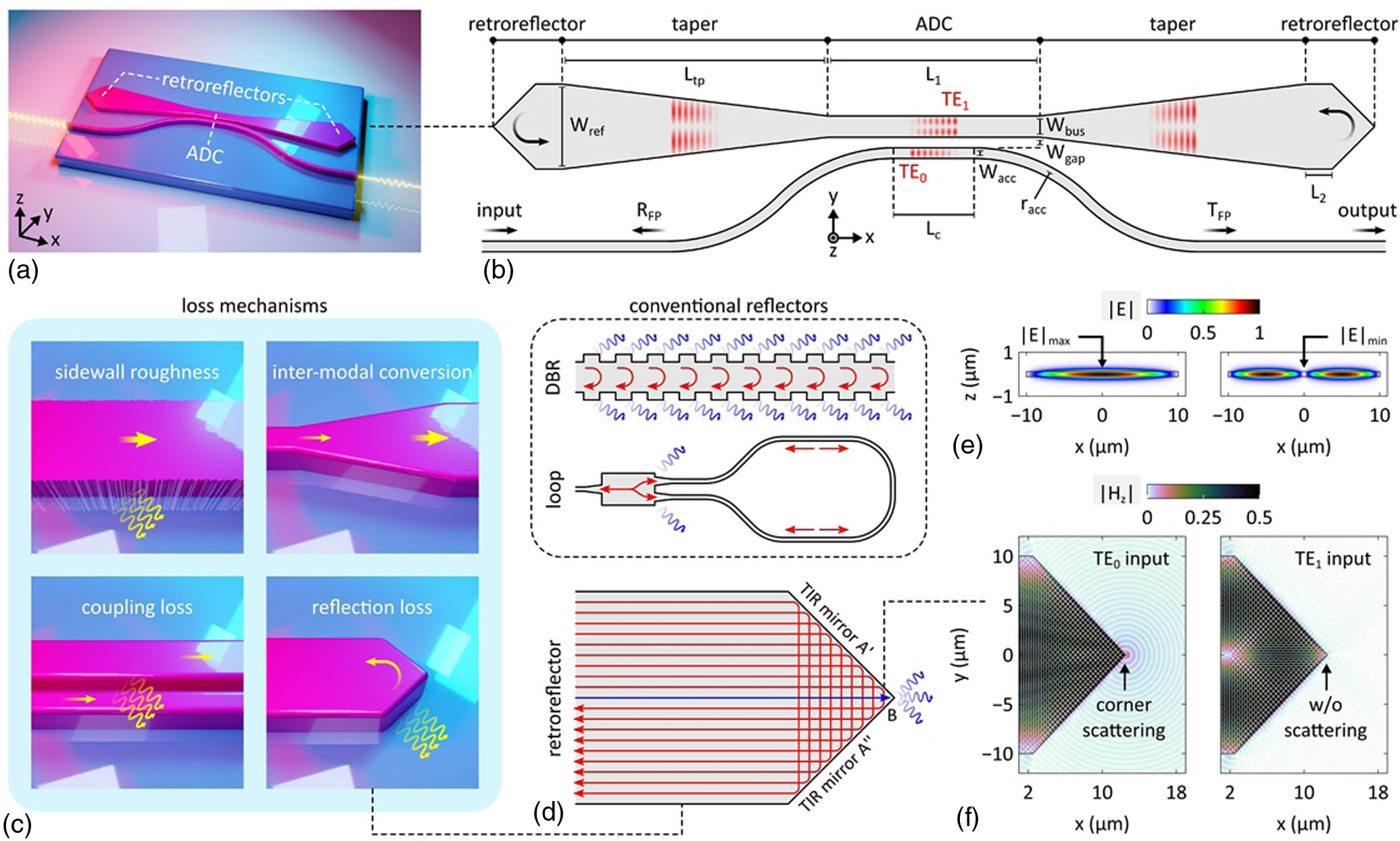
Fig. 1. Conceptual illustration of the FP cavity. (a) 3D view of the FP cavity; (b) schematic configuration of the FP cavity with key parameters labeled. The side coupling is accomplished by using an ADC. The cavity is terminated by a pair of retroreflectors at each end. (c) Illustration of loss mechanisms in the FP cavity; (d) working principle of the retroreflector. Other types of reflectors are also illustrated for comparison. The guided mode in a wide waveguide can be modeled by treating it as a cluster of rays. Each ray will bounce off at mirrors A and A ′ via TIR. The corner scattering at the point B contributes the greatest to reflection losses. (e) Calculated electric field profiles of TE 0 and TE 1 modes; for TE 1 , the field intensity is zero at the central position, thereby depressing the corner scattering completely. (f) Calculated light propagation profiles for the retroreflector when TE 0 and TE 1 modes are launched. The image contrast is enhanced to clearly show the scattering wave. The scattering loss is significantly mitigated when the TE 1 mode is injected.

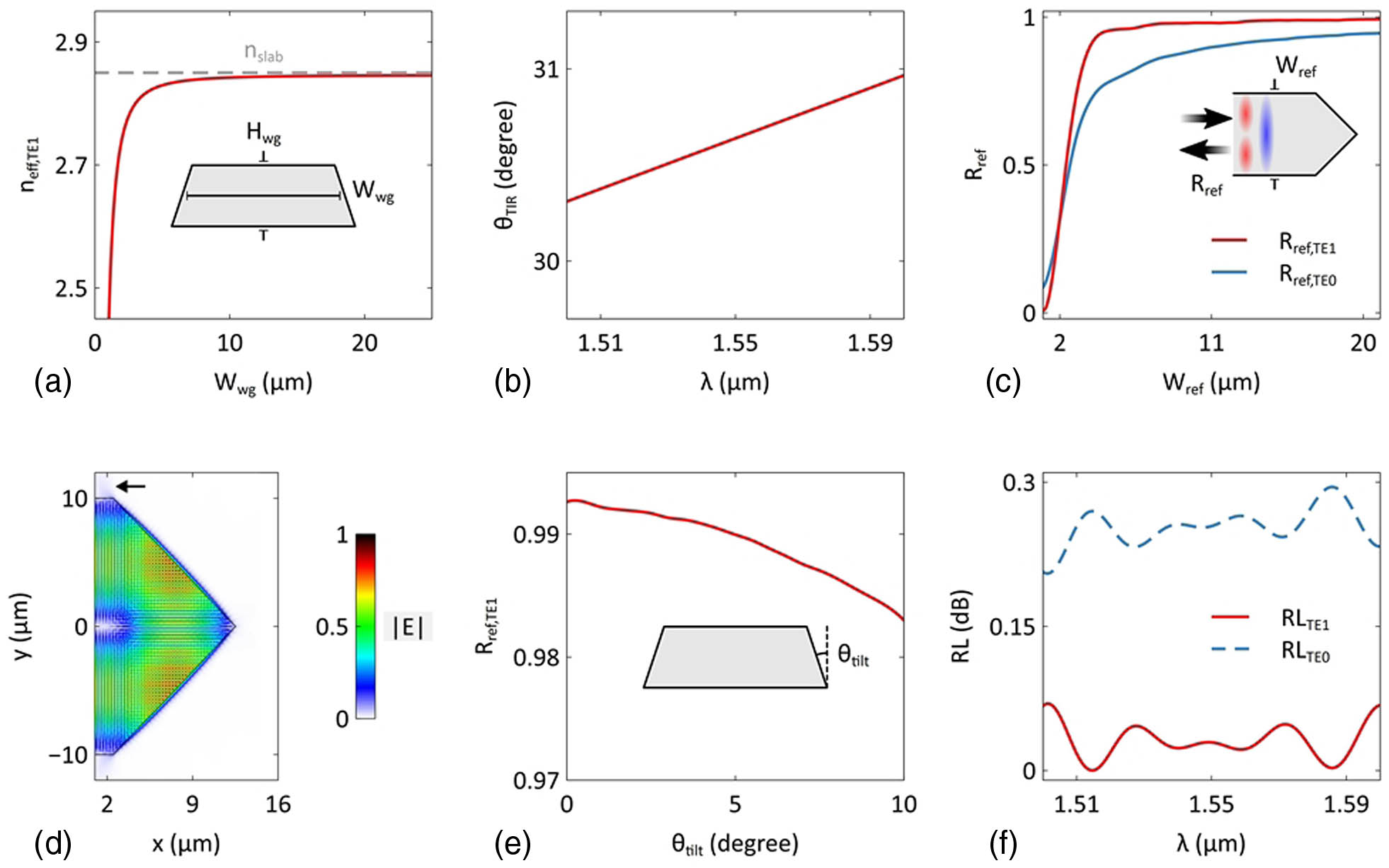
Fig. 2. Analysis and optimization of the retroreflector. (a) Calculated TE 1 effective indices (n eff , TE 1 ) with varying waveguide widths (W wg ). The dashed line represents the effective index of the slab mode (n slab ). The inset shows the waveguide cross section. (b) Calculated TIR angles (θ TIR ) with varying wavelengths; (c) calculated reflectance (R ref , TE 0 , R ref , TE 1 ) with varying retroreflector widths (W ref ). The inset shows the structural top view. The near-unity reflectance can be achieved for TE 1 . (d) Calculated light propagation profile for the optimized retroreflector. The arrow shows the side-scattering effect. (e) Calculated R ref , TE 1 with varying sidewall tilt angles (θ tilt ). The inset shows the waveguide cross section. (f) Calculated TE 1 -reflection-loss (RL TE 1 ) spectrum for the optimized retroreflector. The dashed line shows the calculated TE 0 reflection losses (RL TE 0 ).

Fig. 3. Analysis and optimization of the ADC. (a) Calculated TE 0 and TE 1 effective indices (n eff , TE 0 , n eff , TE 1 ) with varying waveguide widths (W wg ); the dashed lines show the phase matching between TE 0 and TE 1 modes. Calculated coupling-loss (CL) spectra with different (b) widths (W acc ) and (c) bending radii (r acc ) of the accessing waveguide; (d) calculated TE 1 coupling ratio (T CRO , TE 1 ) with varying coupling lengths (L c ). The inset shows the structural top view. (e) Calculated T CRO , TE 1 spectra with different L c ; (f) calculated light propagation profile for the optimized ADC; (g)–(i) calculated intermodal cross talk (XT TE 0 , XT TE 2 , XT TE 3 ) and extinction-ratio (ER TE 0 , ER TE 2 , ER TE 3 ) spectra for the optimized ADC.

Fig. 4. Analysis and optimization of the FP cavity. (a) Calculated TE 1 propagation losses (α TE 1 ) with varying waveguide widths (W wg ) under different mean deviations of sidewall roughness (σ ); (b) calculated transmission efficiencies (T tp , TE i ) with varying taper lengths (L tp ); the inset shows the structural top view. (c) Calculated light propagation profile for the tapered waveguide with L tp = 1.5 mm ; (d) calculated TE 1 effective indices (n eff , TE 1 ) as a two-dimensional map in terms of W wg and wavelengths; calculated (e) mean effective indices (n ˜ eff , TE 1 ) and (f) mean group indices (n ˜ g , TE 1 ) of the TE 1 mode with varying wavelengths; (g) calculated transmittance (T FP ) and reflectance (R FP ) spectra for the FP cavity with L tp = 1.5 mm ; (h) zoom-in view of the T FP spectrum in the vicinity of a single resonance. The red arrow indicates the corresponding spectral position in (g). (i) Calculated loaded Q factors (Q load ) with varying L tp ; the dashed line represents the intrinsic Q factor (Q i ). An ultrahigh intrinsic Q factor of Q i ≈ 4.1 × 10 6 is attained.

Fig. 5. Experimental results for the fabricated FP cavities. (a), (b) Microscopic images of the fabricated devices; the scale bars represent 350 and 200 μm, respectively. (c) Schematic configuration of the measurement setup; (d) measured transmittance (T tp ) spectra with varying taper lengths (L tp ). For clarity, a progressive shift is applied on the plotted spectra. Zoom-in views of the T tp spectra in the vicinity of a single resonance with (e) L tp = 1.5 mm and (f) 4.0 mm; (g) measured loaded Q factors (Q load ) with varying L tp ; (h) reconstructed reflectance (R ref , TE 1 ) and mean-propagation-loss (α ˜ TE 1 ) spectra; (i) measured T FP spectra at different ambient temperatures (t ); (j) measured thermo-optical responses with varying electric power (P ) applied. PC, polarization controller; TEC, thermo-electric cooler; DUT, device under test.

Fig. 6. Calculated TE 1 -coupling ratio (T CRO , TE 1 ) and coupling-loss (CL) spectra with parameter deviations.

Fig. 7. Measured transmittance (T FP ) spectra at different wavelength bands (λ ≈ 1.51 , 1.55, and 1.59 μm) with taper lengths of (a) L tp = 1.5 mm and (b) 4.0 mm; measured (c) extinction ratios (ER res ) and (d) free spectral ranges (FSRs) with varying L tp ; (e) reconstructed TE 1 coupling-ratio (T CRO , TE 1 ) spectrum.
|
Table 1. Performance Comparison of On-Chip FP Cavities

Set citation alerts for the article
Please enter your email address