The monolithic integration of Fabry-Perot cavities has many applications, such as label-free sensing, high-finesse filters, semiconductor lasers, and frequency comb generation. However, the excess loss of integrated reflectors makes it challenging to realize integrated Fabry-Perot cavities working in the ultrahigh- regime (). Here, we propose and experimentally demonstrate what we believe is the first silicon integrated million- Fabry-Perot cavity. Inspired by free-space optics, a novel monolithically integrated retroreflector is utilized to obtain near-unity reflectance and negligible reflection losses. The corner scattering in the retroreflector is prevented by the use of the mode, taking advantage of its zero central field intensity. Losses incurred by other mechanisms are also meticulously engineered. The measurement results show resonances with an ultrahigh intrinsic factor of spanning an 80-nm bandwidth. The measured loaded factor is . Ultralow reflection losses () and propagation losses () are experimentally realized.
1. INTRODUCTION
Fabry-Perot (FP) cavities confine light between a pair of reflectors in the form of a standing wave [1]. Due to its sharp spectral responses and capability for field enhancement, the FP cavity plays a central role in a vast range of applications, e.g., wavemeters [2], gravity-wave detection [3], label-free sensing [4], semiconductor lasers [5], linewidth narrowing [6], quantum-information processing [7], frequency comb generation [8,9], and high-capacity communications [10,11]. Compared to traveling-wave cavities, FP cavities have some unique applications due to the standing-wave property, such as cavity-enhanced optical trapping [12] and atom cooling [13]. In addition, bent waveguides are not required in FP cavities, leading to a smaller footprint and a higher integration density. Silicon-on-insulator (SOI) has become a mainstream platform for photonic integration, thanks to its scalability, high yield, and CMOS compatibility [14]. A variety of FP cavities on SOI have been investigated in recent research [8–11,15–22], but their factors are all quite limited. The photonic-crystal (PhC) nanocavity can offer high factors by trapping the resonant mode in a photonic bandgap [23]. However, the nanocavity mode in PhCs cannot be depicted by FP mechanisms when the cavity length only involves few PhC lattices [24]. Longer FP cavities formed by PhC waveguides have been experimentally characterized, but their factors cannot exceed one million [24,25]. To date, the ultrahigh- () silicon-integrated FP cavity has not yet been demonstrated.
Unlike traveling-wave cavities, such as microring resonators [26,27] and microdisk resonators [28,29], whose intrinsic factors are predominantly governed by propagation loss, FP cavities also suffer from excess losses of reflectors. In order to improve the factor of FP cavities, it is essential to reduce the reflection loss. The distributed Bragg reflector (DBR) is the most commonly used on-chip reflector. The DBR relies on grating structures to form the constructive interference of multiple reflected waves. Typically, DBRs can be realized by introducing sidewall corrugations [8–10,16–18], embedded nanoholes [15], and deep trenches [19,20,30]. However, the requirement for broadband reflection necessitates the use of high-contrast gratings with strong out-of-plane diffraction losses [31]. For a silicon-integrated DBR, such diffraction losses can be as high as 5% [19,30] unless the trench depth is scaled up to several micrometers [20]. Therefore, the factor of most DBR-based FP cavities is restricted to the order of [10,19,20]. In Refs. [8,9], silicon-nitride-on-insulator (SNOI) with a lower index contrast is exploited to alleviate diffraction losses and lift the factor to in a narrow bandwidth, but a higher factor () has remained unattainable. As an alternative, on-chip reflectors can also be built by connecting the output ports of a 3-dB coupler to a looped waveguide [11]. The performance of loop structures is, however, limited by the scattering loss in Y-junctions [32] or multimode interference couplers [33]. The scattering loss can be inhibited by using directional couplers (DCs) [34]. Nevertheless, the coupling ratio of DCs is usually susceptible to fabrication defects and typically has a limited optical bandwidth, making it difficult to attain near-unity reflectance over a broad bandwidth. The reported factor of loop-based FP cavities is limited to [11]. Other types of on-chip reflectors, such as coated metallic mirrors [21] and inverse-designed structures [22], all suffer from the intrinsically high reflection loss caused by ohmic absorption or stringent feature sizes; hence, the measured factors cannot exceed . The ultralow-loss on-chip reflector for ultrahigh- () FP cavities has remained an unsolved open problem.
In this work, we present the first demonstration on million- silicon-integrated FP cavities. Inspired by free-space optics, a nearly lossless retroreflector is developed to address the reflection loss issue. By employing the mode with zero central field intensity, the scattering loss is minimized at the corner region of retroreflectors. Losses from other mechanisms are also reduced to an ultralow level. An ultrahigh intrinsic factor () is experimentally achieved. The maximum loaded factor is measured to be .
Sign up for Photonics Research TOC. Get the latest issue of Photonics Research delivered right to you!Sign up now
2. DESIGN AND ANALYSIS
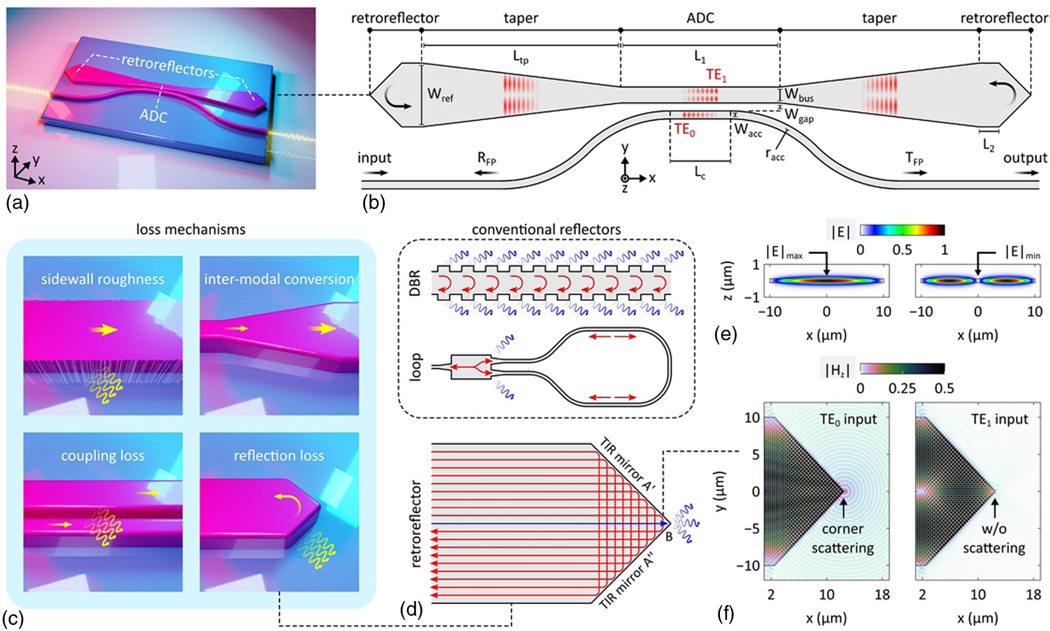
Figures 1(a) and 1(b) depict the schematic configuration of the proposed FP cavity, which consists of an asymmetric directional coupler (ADC) in the middle, a pair of reflectors at each end, and adiabatically tapered waveguides as connectors. The cavity is fed by an accessing waveguide through weak side coupling with a phase shift in the ADC. The tapered waveguide introduces a round-trip group delay, thereby building up a standing-wave resonance in the cavity. The dropped carrier experiences another phase shift, resulting in the total phase shift. At the output port, the destructive interference will dramatically diminish the field intensity for resonant wavelengths, leading to the all-pass filtering of light [21,22]. The on-resonance carriers are reflected back into the input port.
Figure 1.Conceptual illustration of the FP cavity. (a) 3D view of the FP cavity; (b) schematic configuration of the FP cavity with key parameters labeled. The side coupling is accomplished by using an ADC. The cavity is terminated by a pair of retroreflectors at each end. (c) Illustration of loss mechanisms in the FP cavity; (d) working principle of the retroreflector. Other types of reflectors are also illustrated for comparison. The guided mode in a wide waveguide can be modeled by treating it as a cluster of rays. Each ray will bounce off at mirrors and via TIR. The corner scattering at the point contributes the greatest to reflection losses. (e) Calculated electric field profiles of and modes; for , the field intensity is zero at the central position, thereby depressing the corner scattering completely. (f) Calculated light propagation profiles for the retroreflector when and modes are launched. The image contrast is enhanced to clearly show the scattering wave. The scattering loss is significantly mitigated when the mode is injected.
In such a design, loss mechanisms can be categorized into four classes: the propagation loss produced by sidewall roughness, the intermodal conversion in tapered waveguides, the coupling loss in the ADC, and the reflection loss at reflectors, as illustrated in Fig. 1(c). As previously stated, the primary concern is to reduce the reflection loss. Here, we introduce the on-chip retroreflector to realize ultralow-loss reflection, as illustrated in Fig. 1(d). The structure is formed by two total-internal-reflection (TIR) mirrors at an angle of 90°. In a wide waveguide, the guided mode can be approximated as a cluster of weakly divergent rays [35]. Through the TIR effect, each ray will consecutively bounce off at and [36]. Moreover, outer rays strike the mirror earlier than interior rays yet travel a longer transverse distance, resulting in identical light-path lengths for all launched rays. Thus, the input mode can be reflected while preserving its initial phase profile perfectly. The archetype of this structure, well known as the roof prism [37], has served as a fundamental element in numerous free-space optical systems. The retroreflection mechanism is ineffective at the corner point , where mirrors and are joined together, as illustrated in Fig. 1(d). Such corner scattering is the prime cause of reflection losses for on-chip retroreflectors. The mode is employed to tackle this issue. The maximum field intensity of the mode occurs at the central position, as shown in the left panel of Fig. 1(e). In contrast, the central field intensity of the mode is zero, as shown in the right panel of Fig. 1(e). Consequently, the corner scattering can be naturally prevented by choosing the mode to carry resonances. Figure 1(f) shows the calculated light propagation profiles when and modes are injected. For , the corner scattering is significantly mitigated, since all the launched rays reside only on two lateral sides. In the following sections, we will analyze and optimize all the essential components in the proposed FP cavity to achieve an ultrahigh factor.
The design is implemented on the SOI platform consisting of a silicon core with and a silicon-dioxide buffer with μ. The upper cladding is a silicon-dioxide layer with a thickness of μ. The central wavelength is chosen as μ. The reference data for refractive indices can be found in Ref. [38]. We calculate the effective index () with varying widths () by using the finite-difference frequency-domain (FDFD) method [39], as shown in Fig. 2(a). It can be observed that converges to the effective index of the slab mode () when is large enough. Under the ray-optic approximation, the TIR angle () can be obtained by using the equation below, where denotes the refractive index of silicon dioxide. Figure 2(b) shows the calculated dispersion curve of . It can be found that is almost invariant over a 100-nm wavelength range. Thus, the TIR condition (i.e., ) can be fulfilled for mirrors and regardless of working wavelengths.
Figure 2.Analysis and optimization of the retroreflector. (a) Calculated effective indices () with varying waveguide widths (). The dashed line represents the effective index of the slab mode (). The inset shows the waveguide cross section. (b) Calculated TIR angles () with varying wavelengths; (c) calculated reflectance () with varying retroreflector widths (). The inset shows the structural top view. The near-unity reflectance can be achieved for . (d) Calculated light propagation profile for the optimized retroreflector. The arrow shows the side-scattering effect. (e) Calculated with varying sidewall tilt angles (). The inset shows the waveguide cross section. (f) Calculated -reflection-loss () spectrum for the optimized retroreflector. The dashed line shows the calculated reflection losses ().
The reflectance is then calculated for the retroreflector as its width () is varied, as shown in Fig. 2(c). The simulation is carried out by using the finite-difference time-domain (FDTD) method [39]. For comparison, both and are considered in the simulation. The and reflectance (, ) are extracted by applying mode decomposition on the reflected wave [39]. For and , the calculated reflectance rises as increases, suggesting that the lateral divergence of light is mitigated, and the ray-optic approximation is valid. However, for , the maximum reflectance can only reach due to the strong corner scattering. In contrast, for , the near-unity reflectance () can be attained when the width is optimized to be μ. Here, the large modal area is also advantageous for the reduction of propagation losses, since the field intensity is diminished at sidewalls [40]. For a narrower width, e.g., μ, the reflectance is still quite high (), making the proposed reflector well suited for optical filters with smaller footprints and relatively lower factors. Figure 2(d) shows the calculated light propagation profile with μ. From the profile, high reflectance and negligible corner scattering can be observed. A slanted waveguide sidewall may arise because of the difficulty in the precise control of dry-etching processes. The inclination of sidewalls in retroreflectors will introduce excess losses [41]. To address this concern, we also calculate the reflectance as a function of the sidewall tilt angle (), as shown in Fig. 2(e). High reflectance of can still be accomplished, even with a considerably large sidewall tilt angle, e.g., . Such perpendicularity can be ensured by most silicon photonic foundries. The reflection loss () is then calculated to further evaluate the performance, as shown in Fig. 2(f). The calculation results show ultralow reflection losses of for over a 100-nm bandwidth. Around the central wavelength, the reflection loss is reduced by compared to the case. In addition, RL is also slightly affected by the side scattering [see the arrow in Fig. 2(d)], and its strength is tied to the (anti-)node position of lateral standing waves. The ripples in RL spectra are opposite between and , since their symmetries are inversed and the positions of nodes and antinodes are exchanged.
The ADC is leveraged to achieve the side coupling between and . The cross-talk-free -to- conversion relies on the perfect matching between of the accessing waveguide and of the bus waveguide [42]. Figure 3(a) shows the calculated and with varying widths. The combination of accessing-waveguide and bus-waveguide widths (, ) can be then determined according to the phase-matching condition. The coupling loss is calculated for the ADC with various structural parameters, as shown in Figs. 3(b) and 3(c). Here, the coupling loss is defined as , where denotes the remnant transmittance in the accessing waveguide, and denotes the coupling ratio. In the simulation, the gap width is set as to ensure a large feature size and easy gap filling. The coupling loss in an ADC is usually sensitive to the perturbation caused by strong evanescent coupling, since the transmission of higher-order modes is more vulnerable. Therefore, we tend to choose a wide width () to depress the evanescent field intensity and a large bending radius (μ) to ensure the gradual approaching of accessing and bus waveguides, thereby establishing an adiabatic coupling process [26]. According to Fig. 3(a), the bus-waveguide width is then determined as μ. The optimal coupling loss is as low as over a 100-nm wavelength range. Figure 3(d) shows the calculated with varying coupling lengths (). Figure 3(e) shows the corresponding spectra. To enable high- resonances, the coupling length is chosen as μ, with a weak coupling ratio of . Figure 3(f) shows the calculated light propagation profile for the optimized ADC. An efficient -to- conversion and a weak coupling strength can be clearly observed. In total, four TE modes (i.e., ) are supported by the bus waveguide with μ. To verify the mode selectivity, intermodal cross talks () and extinction ratios () are calculated for the optimized ADC [see Figs. 3(g)–3(i)]. Around the central wavelength, low cross talks () and high extinction ratios () can be attained, so that only resonances carried by the mode will be excited in the FP cavity. In addition, high performance can be maintained despite fabrication defects, as detailed in Appendix A.
Figure 3.Analysis and optimization of the ADC. (a) Calculated and effective indices () with varying waveguide widths (); the dashed lines show the phase matching between and modes. Calculated coupling-loss (CL) spectra with different (b) widths () and (c) bending radii () of the accessing waveguide; (d) calculated coupling ratio () with varying coupling lengths (). The inset shows the structural top view. (e) Calculated spectra with different ; (f) calculated light propagation profile for the optimized ADC; (g)–(i) calculated intermodal cross talk (, , ) and extinction-ratio (, , ) spectra for the optimized ADC.
The propagation loss is mainly induced by the sidewall roughness. The volume-current method is used to model this stochastic process by making sidewall nonuniformity as polarized current sources equivalent. The detailed description of this method can be found in Ref. [43]. In Fig. 4(a), we present the calculated propagation losses () with varying under different mean deviations of roughness (). Here, the correlation length of roughness is assumed to be 50 nm [43]. The propagation loss can be reduced to an extremely low level () when the waveguide is quite wide (e.g., μ). In the tapered waveguide, the taper width varies linearly from to ; hence, the taper length () must be carefully designed to avoid the intermodal conversion. Figure 4(b) shows the calculated transmission efficiencies () with varying by using the eigenmode expansion (EME) method. The conversion from to other modes can be fully eliminated (i.e., ) when the taper length is long enough (). The calculated light propagation profile for the tapered waveguide with is shown in Fig. 4(c). Other types of taper trajectories can also be adopted to define the waveguide shape and reduce the device footprint [44]. In this work, it is unnecessary to further shorten the taper length, since the long round-trip length is a desirable attribute in the realization of ultrahigh factors. In a slow-varying taper, light transmission can be described by the following equations [45]: where and denote the magnitudes of electric field at the beginning and end of the tapered waveguide, denotes the vacuum wavenumber, denotes the mean effective index, and denotes the mean propagation loss. Figure 4(d) shows the calculated map in terms of and wavelengths. The spectrum can be then obtained according to Eq. (3), as shown in Fig. 4(e). In addition, we also calculate the corresponding mean group indices (), as shown in Fig. 4(f). By using Eq. (4), the mean propagation loss is calculated to be with at the central wavelength of 1.55 μm. Further calculations show that is nearly wavelength-independent, which is due to the large modal area. Both and are independent with because of the linear taper trajectory. By using Eqs. (3) and (4), the tapered waveguide can be substituted by an equivalent straight waveguide to simplify the modeling of FP cavities.
Figure 4.Analysis and optimization of the FP cavity. (a) Calculated propagation losses () with varying waveguide widths () under different mean deviations of sidewall roughness (); (b) calculated transmission efficiencies () with varying taper lengths (); the inset shows the structural top view. (c) Calculated light propagation profile for the tapered waveguide with ; (d) calculated effective indices () as a two-dimensional map in terms of and wavelengths; calculated (e) mean effective indices () and (f) mean group indices () of the mode with varying wavelengths; (g) calculated transmittance () and reflectance () spectra for the FP cavity with ; (h) zoom-in view of the spectrum in the vicinity of a single resonance. The red arrow indicates the corresponding spectral position in (g). (i) Calculated loaded factors () with varying ; the dashed line represents the intrinsic factor (). An ultrahigh intrinsic factor of is attained.
Eventually, all the essential components in the FP cavity have been optimized. The optimal structural parameters are listed as follows: μ, , μ, , μ, , μ, and μ. Here, and refer to the lengths of straight sections in between retroreflectors and tapers. By using the transient sample mode time-domain (TSMTD) method [39], the transmittance () and reflectance () spectra are obtained for the optimized FP cavity. Here, each component is described by a transfer matrix, which is readily available in Lumerical cosimulation suites [39]. In the simulation, the sidewall roughness is set as , as an example. Figure 4(g) shows the calculated and spectra for the FP cavity with . At resonant wavelengths, the summation of and is nonunity, since a portion of energy is dissipated by intracavity losses. Figure 4(h) is the zoom-in view of the spectrum in the vicinity of a single resonance. The 3-dB bandwidth is calculated to be with the corresponding loaded factor of . A high extinction ratio of can be attained at the resonant wavelength. The calculated rises as increases [see Fig. 4(i)], since the adiabatic taper constitutes the majority of the round-trip length. To determine the intrinsic factor, we also calculate the curve with a reduced coupling length (μ) and a near-zero coupling ratio (). The intrinsic quality factor is estimated to be when the taper length is extended to .
3. FABRICATION AND CHARACTERIZATION
An array of FP cavities with varying was fabricated at Applied Nanotools Inc. [46] by applying electron beam lithography (EBL) and reactive ion etching (RIE) on a commercial SOI wafer, as shown in Figs. 5(a) and 5(b). An oxide upper cladding was deposited through plasma-enhanced chemical vapor deposition (PECVD). Titanium–tungsten heaters were patterned on the top of FP cavities to offer thermo-optical tunability. Efficient edge coupling with lensed fibers is enabled by leveraging inverse tapers [47]. On-chip polarizers were monolithically integrated with inverse tapers to ensure single-polarization operations [48]. Several straight waveguides were fabricated in close proximity for normalization purposes.
Figure 5.Experimental results for the fabricated FP cavities. (a), (b) Microscopic images of the fabricated devices; the scale bars represent 350 and 200 μm, respectively. (c) Schematic configuration of the measurement setup; (d) measured transmittance () spectra with varying taper lengths (). For clarity, a progressive shift is applied on the plotted spectra. Zoom-in views of the spectra in the vicinity of a single resonance with (e) and (f) 4.0 mm; (g) measured loaded factors () with varying ; (h) reconstructed reflectance () and mean-propagation-loss () spectra; (i) measured spectra at different ambient temperatures (); (j) measured thermo-optical responses with varying electric power () applied. PC, polarization controller; TEC, thermo-electric cooler; DUT, device under test.
Figure 5(c) illustrates the measurement setup. The fabricated devices were characterized by scanning the wavelength of a narrow-linewidth tunable laser (Keysight 8164B) while reading the output power from a synchronized high-detectivity power meter (Keysight 81636B). The polarization state was adjusted by a polarization controller (PC). The chip was mounted on a thermo-electric cooler (TEC) to stabilize the ambient temperature. We used an optical isolator to filter out the reflected light, since the performance of an FP cavity can be fully depicted by its spectrum. Figure 5(d) shows the measured spectra around μ with varying . In Figs. 5(e) and 5(f), we show the spectra in the vicinity of a single resonance with and 4.0 mm. By applying Lorentz fitting, loaded factors are characterized to be and , respectively. The measured line shape is virtually symmetric even if the launched laser power is up to , indicating a cold-cavity state and suppressed optothermal responses. This phenomenon originates in the large modal area of multimode waveguides. Numerous applications can benefit from the optothermal stability, such as linewidth narrowing [6] and frequency stabilization [49]. The measured curve is shown in Fig. 5(g). Here, the measurement error is estimated by the standard deviation of obtained from several neighboring resonances. In Appendix B, we also measured the spectra at different wavelength bands. Due to the dispersion of , the measured is higher at shorter wavelengths. In the experiment, we observe a maximum loaded factor of around μ. It is impossible to obtain the intrinsic factor by directly measuring the 3-dB bandwidth of resonances, since the cavity length is constrained by the die size. Here, we propose to use the cavity-scattering theorem to resolve [21]. To achieve this, it is necessary to extract several hidden parameters (i.e., , , and ) from the measured spectra by using the following equations: where FSR denotes the free spectral range, denotes the cavity length (), denotes the mean group index throughout the cavity, and denotes the attenuation over . Three unknown variants (i.e., product, product, and ) can be derived from Eqs. (5)–(7) given the measured , and FSR (see Appendix B). The propagation loss dominates the attenuation process; hence, the product can be formulated as a log-scale linear regression on ,
From Eq. (8), and can be reconstructed by using the intercept and slope of the regression curve. This method is applied at different wavelengths; the reconstruction results are shown in Fig. 5(h). The reflectance is measured to be , with a flattened dispersion over an 80-nm bandwidth. The corresponding reflection loss is , which is in good agreement with the simulation results. The measured propagation loss is . This loss level is quite close to the experimental results demonstrated in Ref. [50]. The reconstructed spectrum is presented in Appendix B. The intrinsic factor is then estimated to be by assuming and in Eq. (5). Figure 5(i) shows the measured spectra at different ambient temperatures (). The temperature sensitivity is measured to be . The thermo-optical tuning was implemented by applying different electric power () with a power source (Keithley 2400), as shown in Fig. 5(j). A high tuning efficiency of is experimentally realized.
4. CONCLUSION AND DISCUSSION
In this work, we report a silicon-integrated FP cavity with an ultrahigh intrinsic factor of . From the measured spectra, we observe a maximum loaded factor of . These results represent the highest factor ever demonstrated in an FP cavity on SOI. The high performance is enabled by a novel on-chip retroreflector working in the multimode regime. The reflectivity of the proposed retroreflector is supported by the naturally low-loss and broadband TIR effect. Moreover, the mode is employed to dampen the corner scattering and bring the reflection loss to an ultralow level. The experimental results provide strong evidence that this new type of reflector possesses ultralow reflection losses () over a broad bandwidth (). The performance of several on-chip FP cavities is summarized and compared in Table 1. The reflection loss of the proposed retroreflector is comparable to that of the bulk DBR with microscale trenches. Compared to the previous results on silicon, the demonstrated factor has been improved by more than 2 orders of magnitude. Usually, such high factors can only be accomplished by using bulky silica waveguides with an ultralow index contrast () [51]. The loaded factor can be further enhanced by decreasing the coupling ratio of ADCs. In addition, it is possible to improve the intrinsic factor through the utilization of more advanced fabrication technologies (e.g., the photonic Damascene process [52]) or material platforms with a lower index contrast (e.g., SNOI) to reduce the sidewall roughness. The reflection loss can be mitigated by using the hard mask in the dry-etching process to improve the perpendicularity of sidewalls [53]. The measured finesse is as high as , which can be improved to by reducing the propagation loss (e.g., ) and coupling ratio (e.g., ).
Performance Comparison of On-Chip FP Cavities
Reference
Platform
Reflector Type
RL [dB]
BW [nm]
FSR [nm]
[dB/cm]
[8]
SNOI
DBR
/
1.39
0.33
/
430
[10]
SOI
DBR
/
/
10.3
/
/
[11]
SOI
Loop
/
1.3
/
19
[15]
SOI
DBR
0.22
80
31.3
/
26
[19]
SOI
DBR
0.32
30
/
/
270
[20]
Bulk Si
DBR
0.03
29.4
1.32
/
500
[21]
SOI
Metallic mirror
0.97
200
21
/
5
[22]
SOI
Inverse design
0.71
200
/
13
This work
SOI
Retroreflector
0.05
0.18
Our design has the potential to serve as a versatile platform for numerous applications, including, but not limited to, comb lasers and linewidth narrowing. The proposed FP cavity possesses an ultrahigh factor and a relatively small free spectral range. These features are desirable for electrically pumped narrow-linewidth dense comb lasers [5]. It is anticipated that a low-threshold low-repetition-rate comb laser could be realized via the heterogeneous integration with thin-filmed III-V gain materials. Another potential application is linewidth narrowing, which is to suppress close-to-carrier noises of lasers by using an ultrahigh- cavity isolated in a cryogenic environment [6]. The large modal volume of the proposed FP cavity could help to mitigate optical nonlinearity and optothermal phase noises [40]. Overall, this work demonstrates a novel method for realizing ultralow-loss on-chip reflectors for the use in ultrahigh- integrated FP cavities, which enriches the silicon photonic toolbox and paves ways for numerous applications.
Acknowledgment
Acknowledgment. The authors acknowledge Applied Nanotools Inc. for enabling the device fabrication. H. Xu thanks ITF Research Talent Hub for the financial support.
APPENDIX A: FABRICATION-TOLERANCE ANALYSIS OF ADCs
The fabricated ADC usually has deviated core dimensions and gap widths as a result of imperfect patterning and etching. In addition, the silicon core thickness is not homogeneous at the wafer scale. Therefore, it is vital to ensure that the designed ADC is immune to these fabrication defects. Figure 6 shows the calculated and CL with , , and . It can be found that the deviation range of is quite small. Ultralow coupling losses of can be also maintained.
Figure 6.Calculated -coupling ratio () and coupling-loss (CL) spectra with parameter deviations.
Figures 7(a) and 7(b) show the measured spectra at different wavelength bands with and 4 mm. The highest loaded factor () is attained around μ. The increasing and decreasing can be observed at shorter wavelengths, which is due to the dispersion of . In Fig. 7(c), the measured extinction ratio ranges from to 2.6 dB as the taper length varies from to 4.5 mm. Figure 7(d) shows the measured curve. The reconstructed spectrum is plotted in Fig. 7(e). At the central wavelength, the coupling ratio is measured to be .
Figure 7.Measured transmittance () spectra at different wavelength bands (, 1.55, and 1.59 μm) with taper lengths of (a) and (b) 4.0 mm; measured (c) extinction ratios () and (d) free spectral ranges (FSRs) with varying ; (e) reconstructed coupling-ratio () spectrum.