
Yanyang Zhou, Linjie Zhou, Haike Zhu, Chiyan Wong, Yida Wen, Lei Liu, Xinwan Li, Jianping Chen. Modeling and optimization of a single-drive push–pull silicon Mach–Zehnder modulator[J]. Photonics Research, 2016, 4(4): 0153
- Photonics Research
- Vol. 4, Issue 4, 0153 (2016)
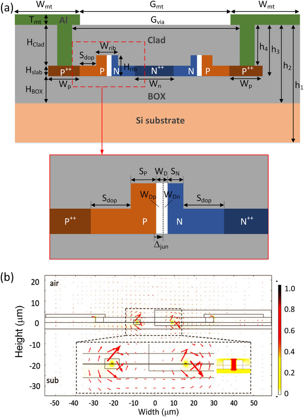
Fig. 1. (a) Cross section of a single-drive push–pull carrier-depletion-based optical modulator. Inset shows the zoom-in of the PN junction. (b) Microwave electrical field distribution in the modulation arms.
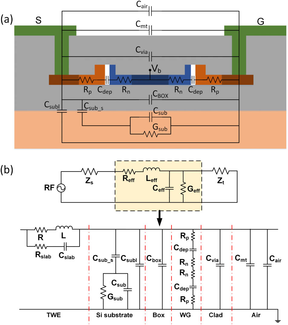
Fig. 2. (a) Electrical components contributed by each layer. (b) Two-port network and the equivalent circuit model of the modulator.
Fig. 3. (a) Calculated L R Z β α S S 21 S 11
Fig. 4. (a) Calculated EO 3 dB bandwidth as a function of metal line width W m t G m t H BOX S dop
Fig. 5. (a) Modulation efficiency V π L V b = 0 V
Fig. 6. (a) Measurement setup to characterize the modulators. (b) Optical microscope image of the MZMs.
Fig. 7. (a) Optical transmission spectra of MZM-2 at 0 and 4 V reverse biases. (b) Modulation efficiency V π L S 21 S 11 S 21
Fig. 8. Measured 56 Gb/s OOK modulation eye diagrams for (a) MZM-1, (b) MZM-2, and (c) MZM-3.
Fig. 9. 40 Gb/s BPSK modulation eye diagrams for (a) MZM-1, (b) MZM-2, and (c) MZM-3.
Fig. 10. Measured 40 Gb/s BPSK modulation BER curves for (a) MZM-2 and (b) MZM-3. Inset shows the constellation diagram.
|
Table 1. Design Parameters for Three MZMs

Set citation alerts for the article
Please enter your email address
© Copyright 2018-2021 | Chinese Laser Press. All Rights Reserved 沪ICP备15018463号-20