Abstract
We present an equivalent circuit model for a silicon carrier-depletion single-drive push–pull Mach–Zehnder modulator (MZM) with its traveling wave electrode made of coplanar strip lines. In particular, the partialcapacitance technique and conformal mapping are used to derive the capacitance associated with each layer. The PN junction is accurately modeled with the fringe capacitances taken into consideration. The circuit model is validated by comparing the calculations with the simulation results. Using this model, we analyze the effect of several key parameters on the modulator performance to optimize the design. Experimental results of MZMs confirm the theoretical analysis. A 56 Gb/s on–off keying modulation and a 40 Gb/s binary phase-shift keying modulation are achieved using the optimized modulator.1. INTRODUCTION
In recent years, the rapid growth of transmission capacity in fiber-optic networks has required optical modulators to possess a large electro-optic (EO) bandwidth to transmit optical signals at high bit rates. Silicon optical modulators based on the free carrier plasma dispersion effect have the unique advantage of monolithic integration with microelectronic circuits on one single chip [1,2]. The carrier-depletion-based silicon Mach–Zehnder modulator (MZM) with the traveling wave electrode (TWE) has been widely investigated over the past decade [3]. Both PN junction and TWE play critical roles in achieving high-speed and high-efficiency modulation. The PN junction needs to be optimized to interact efficiently with the waveguide mode while keeping a low optical loss. Many types of PN junctions have been adopted, such as the interdigitated PN junction [4], the vertical PN junction [5,6], and the PN junction with a compensated region [7,8]. On the other hand, the TWE should be designed to have impedance match, phase match, and low microwave loss to offer a larger EO bandwidth [9–11]. Coplanar waveguides (CPW) and coplanar striplines (CPS) are the two major microwave guiding structures used in the TWE.
In order to design and optimize the PN junction and TWE, finite-element-method (FEM) simulations, which involve complex 2D or 3D device modeling with a fine mesh are routinely used to ensure a high level of accuracy. However, this method lacks efficiency because it needs a long time for numerical calculation and huge computing resources. Moreover, interpretation of the simulation results is sometimes difficult without a clear physical model. Therefore, it is highly demanded to develop a more efficient and physically orientated model to guide silicon modulator design. An equivalent circuit model established based on the device physics can give clear directions for device optimization. Most of the differential-drive silicon modulators adopt the CPW as the TWE [4,10,12,13], and the corresponding equivalent circuit model has been built [14]. The analytical model presented in [14] simplifies the PN junction and does not take into consideration the effect of the fringing electric fields and capacitances, which was later studied theoretically in [15]. Compared with the differential-drive modulators, the single-drive push–pull silicon modulators with a CPS-type TWE [16–19] feature low chirp [20], large bandwidth [19], high linearity [21], and simplified RF interface. The drawback is the increased drive voltage, which is a shortcoming because low voltage is always required to be compatible with CMOS circuits. Nevertheless, such a drive scheme is preferably demanded in implementation of advanced modulation formats such as quadrature phase-shift keying, quadrature amplitude modulation, and N-level pulse amplitude modulation. Hence, it is desired to develop an equivalent circuit model for the single-drive push–pull silicon MZM.
In this paper, we present an equivalent circuit model for the carrier-depletion-based silicon MZM driven by a single-drive push–pull electrode. The device design is optimized based on the model. In Section 2, we present the details of the circuit model, including the CPS TWE and the PN junction. The key features of our model are twofold: (1) the model is derived according to the electrical field distribution in the phase shifter; (2) the model incorporates the microwave loss due to the doped slab layer, which is eliminated by using segmented PN junctions. The derived circuit model is justified by comparing with FEM simulations. In Section 3, we use the circuit model to optimize the TWE and the segmented PN junction to enlarge the EO bandwidth while reducing the microwave loss. The doping concentration is also separately optimized by using FEM simulation to achieve high modulation efficiency. In Section 4, we present the measured performance of the MZMs. The S-parameter measurements show that the modulator with segmented PN junctions suffers a lower microwave loss in the high RF frequency end. The EO bandwidth of the optimized modulator is 33 GHz at 4 V reverse bias. On–off keying (OOK) modulation at the data of 56 Gb/s is realized with an extinction ratio (ER) of 4 dB and a -factor of 3.73. Binary phase-shift keying (BPSK) modulation is also realized at 40 Gb/s with the bit error rate (BER) below the forward error correction level.
Sign up for Photonics Research TOC. Get the latest issue of Photonics Research delivered right to you!Sign up now
2. EQUIVALENT CIRCUIT MODEL
Figure 1(a) shows the cross section of the active arms driven by the CPS-TWE of the silicon MZM. PN junctions are embedded in the silicon-on-insulator rib waveguides. The waveguide has a width , a height , and a remaining slab height . The PN junction is located in the waveguide center with a lateral offset toward the N-doped side. Highly doped regions are separated from the waveguide sidewalls with a distance to reduce free-carrier absorption loss. The doping regions are connected to the signal and ground metal lines of the CPS-TWE, respectively. A DC bias is applied to the middle doping region to set the two PN junctions in a reverse bias mode. We adopt the asymmetric MZI structure because the bias point needed for OOK and BPSK modulations can be conveniently set by tuning the input laser wavelength. Figure 1(b) shows the calculated electric field distribution of the microwave drive signal, which is helpful to establish the equivalent circuit model. As the electric field is distributed in all layers, we will consider the contribution of each layer to the entire circuit.
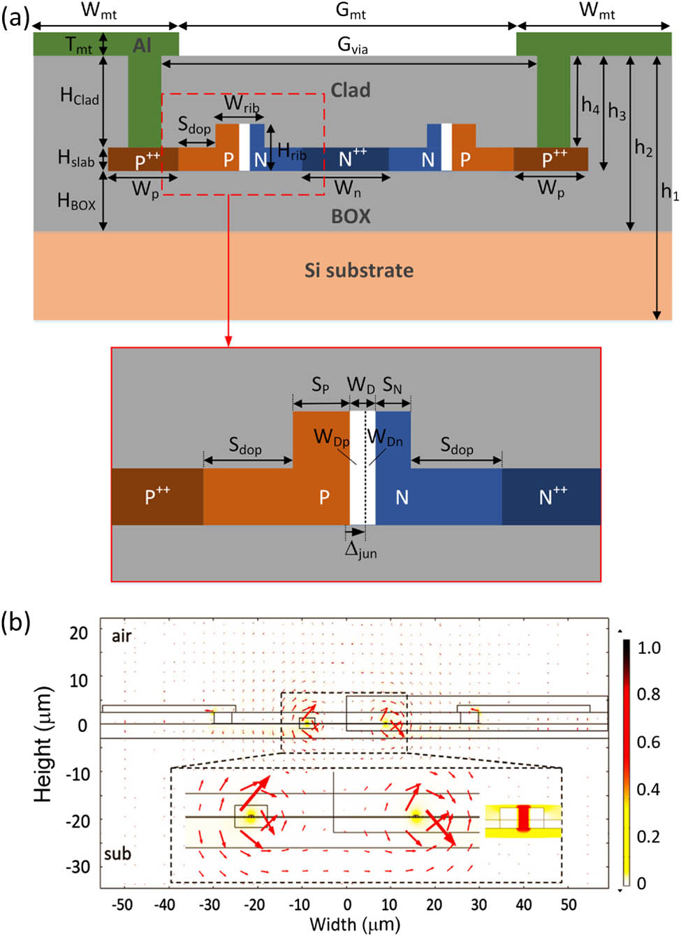
Figure 1.(a) Cross section of a single-drive push–pull carrier-depletion-based optical modulator. Inset shows the zoom-in of the PN junction. (b) Microwave electrical field distribution in the modulation arms.
Figure 2(a) shows the equivalent circuit model of the CPS-TWE in each layer. Figure 2(b) depicts the two-port transmission line model where the CPS-TWE can be represented by the characteristic impedance () and the propagation constant (). In order to achieve a high EO bandwidth, should be equal to the source impedance () and the terminal impedance (), eliminating the microwave signal backreflection. Generally, in the conventional microwave communication system, and are 50 Ω. The microwave effective refractive index () should be close to the group refractive index of the waveguide optical mode () to synchronize the electrical and optical waves. The microwave attenuation factor () is a key parameter to determine the electro–electro (EE) bandwidth of the TWE. Both and can be deduced from .

Figure 2.(a) Electrical components contributed by each layer. (b) Two-port network and the equivalent circuit model of the modulator.
Based on the partial-capacitance technique and the conformal mapping, we can derive the capacitance associated with each layer. We use the theoretical derivation in [22] to calculate the capacitances. The geometrical factor for a conformal mapped air-filled CPS is defined as follows: where is the complete elliptic integral of the first kind, is the argument of the integral (, 1, 2, 3, 4) and , is the thickness denoted in Fig. 1(a), is the gap size between the two metal lines, and is the metal width. The capacitances contributed by each layer can be expressed using the geometrical factor.
The behavior of the silicon substrate is described by a conductor and a capacitor connected in parallel [23]: where is the conductivity of the silicon substrate, is the permittivity in vacuum, and is the silicon relative permittivity. A capacitor is used to represent the capacitance between the signal metal strip and the Si substrate, given by where is the silicon dioxide relative permittivity. An auxiliary capacitor is present to make the total capacitance converge to at the high-frequency limit [14]. Therefore, we have the following expression:
The capacitance of the BOX layer is given by
According to [15], the PN junction depletion capacitance is made of four parts: the ideal depletion capacitance , the fringe capacitance due to the charges at the center of the diode, and the fringe capacitances and due to extended depletion widths at the top and bottom surfaces of the waveguide, respectively. These constituent capacitances are expressed as where is the center depletion region width, and is the depletion widths in the and sides of the diode calculated using . The depletion width can be approximated from 1D PN diode model as where is the carrier concentration in regions, is the built-in potential of the junction, is the bias voltage on the junction, is the fundamental electron charge, is the Boltzmann constant, and is the ambient temperature. The impedance due to the lightly doped slab and rib sections is given by where is the mobility of the , -doped silicon, and is the microwave frequency.
The capacitance between the two metal vias in the upper cladding layer is modeled by a parallel plate capacitance:
Similarly, the capacitance formed between the signal and ground metal lines is expressed as
The capacitance in the air space outside the chip is expressed as
At the high microwave frequencies, the longitudinal current flows along the transmission lines and highly doped slabs [24]. The resistance of the slab per unit length, , is expressed as where is the conductivity of the -doped slabs. In order to reduce the microwave loss due to the doped slab, we can use a segmented PN junction (e.g., a 1 μm long striation undoped in every 10 μm long PN junction) to ensure that current flows only in the metal strips [25]. This undoped striation forms an extra capacitance in the slab. The capacitance per unit length, , is expressed as where is the undoped striation width and is the period of segmented PN junction.
The longitudinal current flow in the metal strips is represented as the resistance in series with the inductance . According to electrical field distribution in the CPW and CPS structures, the CPS can be regarded as one half of CPW. The and are expressed as where and can be calculated by the formulas given in [26]. The longitude current also flows in the substrate, which is ignored because the resistance of substrate is much larger than the highly doped slabs [27].
The above constituent circuit components can be transformed to a simple transmission line model with effective components , , , , as shown in Fig. 2(b). The complex characteristic impedance and the complex propagation constant are expressed as
The average voltage that drops across the signal and ground metal lines is given by [14] where is the drive signal voltage amplitude, is its modulation frequency, and is the length of the TWE. The average voltage formula in Eq. (29) has taken into account the velocity match, impedance match, and the microwave loss. Any velocity mismatch and impedance mismatch will reduce the accumulated interaction between microwave and optical wave. Based on the and , the -parameters of the TWE are expressed as where and are reflections at the input and load ends, respectively, given by where is the TWE input impedance, given by
The voltage useful for modulation is the voltage drop on the PN junctions:
Therefore, the modulator frequency response can be expressed as the junction voltage normalized to its low-frequency () value:
As a first-order approximation, the EO response is directly related to . The 3 dB EO bandwidth is reached when .
In order to verify the validity of the equivalent circuit model, we compare the analytical modeling results with the numerical simulation results by the commercial software COMSOL Multiphysics, which uses the FEM to solve Maxwell’s equations. The MZM design was described in detail in our previous work [17]. The device parameters are , , , , , , , , , , , , , , , , and .
Figure 3(a) shows the calculated and of the TWE using Eqs. (25) and (26). Figure 3(b) illustrates the real and imaginary parts of the characteristic impedance as a function of microwave frequency. The relative error of is less than 9%. The discrepancy in between the calculation and simulation at the low frequency end may probably come from the errors in solving the RF eigenmode by COMSOL Multiphysics where the electromagnetic field is weekly confined in the TWE at the low frequencies. At the high-frequency end, the discrepancy is possibly due to the inaccuracy in calculating the resistances because the skin effect becomes more severe toward the high frequency. Figure 3(c) depicts the microwave propagation constant and attenuation change with frequency. We further compare the EE -parameters between calculation and simulation, as shown in Fig. 3(d). The overall good agreement verifies the validity of the TWE model.
Figure 3.(a) Calculated and as a function of frequency. Comparison between calculation and simulation results for (b) characteristic impedance (), (c) propagation constant () and microwave attenuation (), and (d) EE -parameters ( and ).
3. DEVICE OPTIMIZATION
The equivalent circuit model can provide us with clear physical insight into the TWE. We use the model to further optimize the MZM. We first study the influence of metal line dimensions and on the MZM EO bandwidth [Fig. 4(a)]. The other parameters remain unchanged. It is revealed that should be reduced and should be around to 30 μm in order to have a higher EO bandwidth. We next explore the effect of the buried oxide (BOX) layer thickness [Fig. 4(b)]. The BOX layer has a slight impact on microwave loss, characteristic impedance, and microwave effective index; hence, we will not take it into prime consideration in our optimization. It is clear that has a significant influence on all three parameters [Fig. 4(c)]. A lower microwave loss is achieved by using a smaller , accompanied by reduced impedance and increased microwave refractive index. According to Eq. (16), a smaller leads to a lower series impedance and, therefore, a higher EO bandwidth as suggested by Eqs. (39) and (40). The simulation results show the MZM with segmented PN junction can have less microwave attenuation as shown in Fig. 4(d).
Figure 4.(a) Calculated EO 3 dB bandwidth as a function of metal line width and gap separation . (b) Effect of BOX layer thickness on the TWE characteristics. (c) Effect of doping separation on the TWE characteristics. (d) Microwave attenuation of the MZMs designed with a single or a segmented PN junction.
Doping concentrations and of the PN junctions are another two key parameters to affect the modulator performance. Here we use the COMSOL software to simulate the modulation efficiency and the optical loss change with and with the DC bias , as shown in Fig. 5. Here the small-signal is calculated from the following equation: where is the effective refractive index of the silicon waveguide. The modulation efficiency can be improved by increasing the P and N doping concentrations, as shown in Fig. 5(a). It should be noted that the overlap between the free-carrier depletion and the optical mode determines the waveguide effective refractive index change. The donor/acceptor concentration change will affect the electron/hole concentration and the depletion width. The combined effect on the waveguide modal index can only be solved numerically. The optical loss also increases with the higher doping concentrations, as shown in Fig. 5(b). The trade-off between modulation efficiency and optical loss should be taken into consideration. Here we choose and . The simulation results show that and the doping-induced optical loss is 5.54 dB for the 3 mm long active arm.
Figure 5.(a) Modulation efficiency and (b) optical loss versus PN junction doping concentrations at .
4. EXPERIMENT
We designed three MZMs with different design parameters, as shown in Table 1. The design of MZM-1 follows the previous work reported in [17]. The three key parameters of the TWE (, , and ) are further optimized using our model, as described in the previous section, and the resulting device is denoted as MZM-2. In order to investigate the effect of the segmented PN junction, we also designed a modulator MZM-3 with the same set of parameters as MZM-1, but the PN junction is segmented with a 1 μm long striation undoped in every 10 μm long PN junction.
| Device | PN Junction | Wmt(μm) | Gmt(μm) | Wn(μm) | Wp(μm) |
| MZM-1 | Regular | 60 | 50 | 16.2 | 20.7 |
| MZM-2 | Regular | 40 | 28 | 14 | 10.8 |
| MZM-3 | Segmented | 60 | 50 | 16.2 | 20.7 |
Table 1. Design Parameters for Three MZMs
Figure 6 shows the experimental setup to characterize the modulators. A pulse pattern generator (PPG N4975A) was used to generate a pseudo-random binary sequence (PRBS) drive signal with a pattern length. The drive signal was amplified and fed into the TWE via a 40 GHz microwave probe. The other end of the TWE was terminated with external 50 ohm resistors via another microwave probe. A bias voltage was applied to the heavily doping region via a DC probe. A tunable continuous wave (CW) laser was used as the light source. The light was set to the transverse electric (TE) polarization by using a polarization controller before launching into the chip. On-chip inverse tapers were used for optical input and output coupling. The modulated optical signal from the chip was fed into an optical modulation analyzer (OMA N4392A) for constellation diagram measurement. Alternatively, it was first amplified by an erbium-doped optical fiber amplifier (EDFA) followed by a 3 nm bandwidth optical filter and then collected by a Keysight digital signal analyzer (DSA-X 93204A) for eye diagram measurement.
Figure 6.(a) Measurement setup to characterize the modulators. (b) Optical microscope image of the MZMs.
A. Characterization of the Modulators
The measured optical transmission spectra of the MZM-2 at 0 and 4 V reverse bias are shown in Fig. 7(a). The optical responses of the other two designs are similar. The free spectra range (FSR) is 6.4 nm. The peak transmission of 9.5 dB represents the on-chip insertion loss of the modulator, including about 8 dB waveguide loss and 1.5 dB loss from the two multimode interferometers that compose the MZI. The is 5.4 and 4.95 V for the top and bottom arms, respectively. The measured modulation efficiency is shown in Fig. 7(b). at is and for the top and bottom arms, respectively. The measured agrees well with the simulation result, as presented in Section 3. The modulation efficiency is dependent on the DC bias voltage, so the DC bias needs to be carefully set in order to balance the modulation efficiency and speed. A low DC bias results in a small and hence low microwave drive voltage, but the junction capacitance is also high, which is unfavorable for high-speed modulation. On the contrary, a high DC bias improves the modulation speed, but the modulation efficiency is low; therefore, a large microwave voltage swing is required.
Figure 7.(a) Optical transmission spectra of MZM-2 at 0 and 4 V reverse biases. (b) Modulation efficiency of MZM-2. (c) Real part of the characteristic impedance. (d) Imaginary part of the characteristic impedance. (e) Microwave transmission response EE . (f) Microwave reflection response EE . (g) Modulator frequency response EO .
Before characterization of the TWE, the microwave probe and coaxial cables were calibrated by using the standard short-open-load-through method. Figures 7(c) and 7(d) show the characteristic impedance of the TWE for three different designs. Low microwave reflection requires the characteristic impedance close to . The measured EE -parameters of the TWE at are shown in Figs. 7(e) and 7(f). According to [11], when the RF phase velocity is well-matched with the optical wave group velocity, the 3 dB EO bandwidth is given by the 6.4 dB EE bandwidth. The 6.4 dB EE bandwidth of all MZMs are above 25 GHz. Compared with MZM-1, MZM-3 presents a higher EE bandwidth, indicating that the segmented PN junction can effectively reduce the microwave loss. Return loss () of the TWE indicates the microwave reflection at the entrance of the TWE due to impedance mismatch. The of all MZMs are below , suggesting very low reflection from the 10 MHz to 32 GHz frequency range. Figure 7(g) shows the measured EO response of the modulator by using a lightwave component analyzer (LCA), which covers the frequency range from 100 MHz to 40 GHz. The electrical ports of the LCA were calibrated by the standard SLOT method. The EO 3 dB bandwidth of MZM-1 at is 29 GHz. The MZM-2 has an improved EO bandwidth of 33 GHz due to the optimization of the TWE. Comparing MZM-1 and MZM-3, we notice that the latter one with a segmented PN junction exhibits a slower roll-off, due to the low microwave attenuation [see Fig. 4(d)]. To further improve the modulator performance, the TWE in MZM-2 could also be segmented.
B. High-Speed OOK and BPSK Modulations
We first performed the OOK modulation using the three modulators. The RF drive signal was a 56 Gb/s PRBS signal amplified to a 7.8 V peak-to-peak voltage. A 6 V DC bias was simultaneously applied to the MZM. The input laser wavelength was set at the quadrature point of the MZI. The measured 56 Gb/s OOK modulation eye diagram of these MZMs are shown in the Figs. 8(a)–8(c). The top curves in each graph are the clock signal and the modulated optical waveforms. It can be seen that MZM-2 presents a better eye diagram than the other two. The measured ER is 4.0 dB, and the -factor is 3.73.
Figure 8.Measured 56 Gb/s OOK modulation eye diagrams for (a) MZM-1, (b) MZM-2, and (c) MZM-3.
We next carried out the BPSK modulation. The laser wavelength was tuned to the minimum transmission point, and the DC bias was set to . Figure 9 shows the eye diagrams of the 40 Gb/s BPSK modulation. The measured BER of MZM-2 is shown in Fig. 10(a). The inset shows the constellation diagram when the optical signal-to-noise-ratio is 15.56 dB. The BPSK signal magnitude and phase errors are 18.9% and 6.9°, respectively, and the error vector magnitude (EVM) is around 22%. The -factor is 6.6. The BER deduced from the measured EVM is . The BER can be decreased by increasing the received optical power. All the measured BER are below the requirement in forward error correction techniques. The measured BER and constellation diagram of MZM-3 are shown in the Fig. 10(b). It has a similar modulation performance with MZM-2.
Figure 9.40 Gb/s BPSK modulation eye diagrams for (a) MZM-1, (b) MZM-2, and (c) MZM-3.
Figure 10.Measured 40 Gb/s BPSK modulation BER curves for (a) MZM-2 and (b) MZM-3. Inset shows the constellation diagram.
A low drive voltage is required in order for the modulators to be compatible with CMOS drive circuits. The drive voltage can be lowered with an improved modulation efficiency either by increasing the doping concentration or designing a PN junction that can provide more depletion overlap with the waveguide mode. Interleaved PN junctions [4] or L-shaped/U-shaped PN junctions [28] could be used to ensure a low . In order to obtain a high EO bandwidth, the silicon substrate can even be etched off to give a better phase match between the RF mode and the optical mode [29].
5. CONCLUSION
We have established an equivalent circuit model for the CPS-TWE in a single-drive push–pull silicon modulator. The partial-capacitance technique and conformal mapping were used to calculate the capacitance contributed by each layer. Fringe capacitances were taken into consideration to accurately model the PN junction. The accuracy of the equivalent circuit model was justified by comparing with numerical simulations. Based on this model, we optimized the key parameters in TWE design to achieve a large EO bandwidth. The segmented PN junction design was proved to be efficient in reducing the microwave loss. The doping concentrations were chosen to make a compromise between modulation efficiency and optical loss. The 3 dB EO bandwidth of the optimized 3 mm long MZM was measured to be 33 GHz at 4 V reverse bias. 56 Gb/s OOK and 40 Gb/s BPSK modulations have been successfully demonstrated.
Acknowledgment
Acknowledgment. We also thank IME Singapore for device fabrication.
References
[1] G. T. Reed, G. Z. Mashanovich, F. Y. Gardes, D. J. Thomson. Silicon optical modulators. Nat. Photonics, 4, 518-526(2010).
[2] T. Y. Liow, K. W. Ang, Q. Fang, J. F. Song, Y. Z. Xiong, M. B. Yu, G. Q. Lo, D. L. Kwong. Silicon modulators and germanium photodetectors on SOI: monolithic integration, compatibility, and performance optimization. IEEE J. Sel. Top. Quantum Electron., 16, 307-315(2010).
[3] G. T. Reed, G. Z. Mashanovich, F. Y. Gardes, M. Nedeljkovic, Y. Hu, D. J. Thomson, K. Li, P. R. Wilson, S.-W. Chen, S. S. Hsu. Recent breakthroughs in carrier depletion based silicon optical modulators. Nanophotonics, 3, 229-245(2014).
[4] H. Xu, X. Y. Li, X. Xiao, Z. Y. Li, Y. D. Yu, J. Z. Yu. Demonstration and characterization of high-speed silicon depletion-mode Mach–Zehnder modulators. IEEE J. Sel. Top. Quantum Electron., 20, 23-32(2014).
[5] D. J. Thomson, F. Y. Gardes, S. Liu, H. Porte, L. Zimmermann, J. M. Fedeli, Y. F. Hu, M. Nedeljkovic, X. Yang, P. Petropoulos, G. Z. Mashanovich. High performance Mach–Zehnder-based silicon optical modulators. IEEE J. Sel. Top. Quantum Electron., 19, 85-94(2013).
[6] S. S. Azadeh, F. Merget, S. Romero-García, A. Moscoso-Mártir, N. von den Driesch, J. Müller, S. Mantl, D. Buca, J. Witzens. Low Vπ silicon photonics modulators with highly linear epitaxially grown phase shifters. Opt. Express, 23, 23526-23550(2015).
[7] X. Tu, T.-Y. Liow, J. Song, X. Luo, Q. Fang, M. Yu, G.-Q. Lo. 50-Gb/s silicon optical modulator with traveling-wave electrodes. Opt. Express, 21, 12776-12782(2013).
[8] K. Goi, A. Oka, H. Kusaka, Y. Terada, K. Ogawa, T.-Y. Liow, X. Tu, G.-Q. Lo, D.-L. Kwong. Low-loss high-speed silicon IQ modulator for QPSK/DQPSK in C and L bands. Opt. Express, 22, 10703-10709(2014).
[9] R. Ding, Y. Liu, Y. J. Ma, Y. S. Yang, Q. Li, A. E. J. Lim, G. Q. Lo, K. Bergman, T. Baehr-Jones, M. Hochberg. High-speed silicon modulator with slow-wave electrodes and fully independent differential drive. J. Lightwave Technol., 32, 2240-2247(2014).
[10] J. F. Ding, R. Q. Ji, L. Zhang, L. Yang. Electro-optical response analysis of a 40 Gb/s silicon Mach-Zehnder optical modulator. J. Lightwave Technol., 31, 2434-2440(2013).
[11] M. Streshinsky, R. Ding, Y. Liu, A. Novack, Y. Yang, Y. Ma, X. Tu, E. K. S. Chee, A. E.-J. Lim, P. G.-Q. Lo. Low power 50 Gb/s silicon traveling wave Mach–Zehnder modulator near 1300 nm. Opt. Express, 21, 30350-30357(2013).
[12] D. Thomson, F. Gardes, Y. Hu, G. Mashanovich, M. Fournier, P. Grosse, J. Fedeli, G. Reed. High contrast 40 Gbit/s optical modulation in silicon. Opt. Express, 19, 11507-11516(2011).
[13] J. Wang, C. Qiu, H. Li, W. Ling, L. Li, A. Pang, Z. Sheng, A. M. Wu, X. Wang, S. C. Zou, F. W. Gan. Optimization and demonstration of a large-bandwidth carrier-depletion silicon optical modulator. J. Lightwave Technol., 31, 4119-4125(2013).
[14] H. Yu, W. Bogaerts. An equivalent circuit model of the traveling wave electrode for carrier-depletion-based silicon optical modulators. J. Lightwave Technol., 30, 1602-1609(2012).
[15] H. Jayatilleka, W. D. Sacher, J. K. S. Poon. Analytical model and fringing-field parasitics of carrier-depletion silicon-on-insulator optical modulation diodes. IEEE Photon. J., 5, 2200211(2013).
[16] P. Dong, L. Chen, Y.-k. Chen. High-speed low-voltage single-drive push-pull silicon Mach-Zehnder modulators. Opt. Express, 20, 6163-6169(2012).
[17] J. T. Wang, L. J. Zhou, H. K. Zhu, R. Yang, Y. Y. Zhou, L. Liu, T. Wang, J. P. Chen. Silicon high-speed binary phase-shift keying modulator with a single-drive push-pull high-speed traveling wave electrode. Photon. Res., 3, 58-62(2015).
[18] H. K. Zhu, L. J. Zhou, T. Wang, L. Liu, C. Y. Wong, Y. Y. Zhou, R. Yang, X. W. Li, J. P. Chen. Optimized silicon QPSK modulator with 64-Gb/s modulation speed. IEEE Photon. J., 7, 1-6(2015).
[19] M. Chagnon, M. Morsy-Osman, M. Poulin, C. Paquet, S. Lessard, D. V. Plant. Experimental parametric study of a silicon photonic modulator enabled 112-Gb/s PAM transmission system with a DAC and ADC. J. Lightwave Technol., 33, 1380-1387(2015).
[20] L. Chen, P. Dong, Y. K. Chen. Chirp and dispersion tolerance of a single-drive push-pull silicon modulator at 28 Gb/s. IEEE Photon. Technol. Lett., 24, 936-938(2012).
[21] Y. Zhou, L. Zhou, F. Su, J. Xie, H. Zhu, X. Li, J. Chen. Linearity measurement of a silicon single-drive push-pull Mach-Zehnder modulator. Conference on Lasers and Electro-Optics (CLEO): Science and Innovations, SW3N-6(2015).
[22] E. L. Chen, S. Y. Chou. Characteristics of coplanar transmission lines on multilayer substrates: modeling and experiments. IEEE Trans. Microwave Theory Tech., 45, 939-945(1997).
[23] V. Milanovic, M. Ozgur, D. C. DeGroot, J. A. Jargon, M. Gaitan, M. E. Zaghloul. Characterization of broad-band transmission for coplanar waveguides on CMOS silicon substrates. IEEE Trans. Microwave Theory Tech., 46, 632-640(1998).
[24] Y. R. Kwon, V. M. Hietala, K. S. Champlin. Quasi-TEM analysis of ‘slow-wave’ mode propagation on coplanar microstructure MIS transmission lines. IEEE Trans. Microwave Theory Tech., 35, 545-551(1987).
[25] T. Baehr-Jones, R. Ding, Y. Liu, A. Ayazi, T. Pinguet, N. C. Harris, M. Streshinsky, P. Lee, Y. Zhang, A. E.-J. Lim. Ultralow drive voltage silicon traveling-wave modulator. Opt. Express, 20, 12014-12020(2012).
[26] W. Heinrich. Quasi-TEM description of MMIC coplanar lines including conductor-loss effects. IEEE Trans. Microwave Theory Tech., 41, 45-52(1993).
[27] D. Petousi, L. Zimmermann, A. Gajda, M. Kroh, K. Voigt, G. Winzer, B. Tillack, K. Petermann. Analysis of optical and electrical tradeoffs of traveling-wave depletion-type Si Mach–Zehnder modulators for high-speed operation. IEEE J. Sel. Top. Quantum Electron., 21, 199-206(2015).
[28] K. Goi, N. Ishikura, H. Ishihara, S. Sakamoto, K. Ogawa, T.-Y. Liow, X. Tu, G.-Q. Lo, D. L. Kwong. Low-voltage silicon Mach-Zehnder modulator operating at high temperatures without thermo-electric cooling. Optical Fiber Communication Conference, W2A–23(2016).
[29] X. Xiao, M. Li, Z. Li, L. Wang, Q. Yang, S. Yu. Substrate removed silicon Mach-Zehnder modulator for high baud rate optical intensity modulations. Optical Fiber Communication Conference, Th4H-5(2016).

