Abstract
We propose a novel silicon optical phase shifter structure based on heterogeneous strip-loaded waveguides on a photonic silicon on insulator (SOI) platform. The features of an etchless SOI layer and loaded strip would enhance the performance and uniformity of silicon optical modulators on a large-scale wafer. We implemented the phase shifter by loading an amorphous silicon strip onto an SOI layer with a vertical PN diode structure. Compared to the conventional lateral PN phase shifter based on half-etched rib waveguides, this phase shifter shows a >1.5 times enhancement of modulation efficiency and provides >20 GHz high-speed operation.1. INTRODUCTION
Silicon optical modulators are key components in silicon photonic transceivers for short-reach optical interconnects and telecommunications applications. In silicon, the free carrier dispersion effect is the only practical mechanism for realizing high-speed modulators. At present, the three main types of optical phase shifters for modulators are the capacitor type [1,2], carrier-injection type [3–5], and carrier-depletion type [6–16]. Among these, the carrier-depletion-type phase shifters are the ones mainly used for high-speed silicon modulators. Extensive effort has been made to improve the modulation efficiency and achieve low-voltage and low-power driving. The modulation efficiency is determined by the overlap between the optical field and the depletion region, which can be tuned by applying reverse bias. A depletion-type phase shifter usually has three types of diodes—vertical PN [6], horizontal PN [7–13], and orthogonal interleaved PN [14,15]—normally formed in half-etched rib waveguides to provide electrical connection to electrodes. Various PN junction structures based on such rib waveguides have been proposed with the intention of enhancing the overlap between the optical mode and depletion region. For a rib waveguide, however, it is difficult to precisely control the rib height (i.e., etching depth) due to the dry-etching process. Fluctuation in rib height will induce a deviation in optical confinement and thus cause variation in modulation efficiency. Moreover, the thickness difference between the rib and slab makes it impossible to achieve a uniform doping profile, which is believed to be important for increasing efficiency.
To address these two issues, we propose a strip-loaded waveguide-based phase shifter on a photonic silicon on insulator (SOI) layer without any etching of the top silicon layer. In this phase shifter, the SOI layer retains its flatness and ions are implanted before the strip-loaded waveguide is formed so that a uniform doping profile can be easily achieved. In the waveguide, optical confinement is provided in the SOI layer by the upper loaded strip, which can be precisely fabricated by etching because an etching endpoint exists between the heterogeneous materials.
In this paper, we first explain the concept of the novel phase shifter for a silicon modulator. Then we describe the characteristics of the strip-loaded phase shifter employing hydrogenated amorphous silicon (a-Si:H) as the strip material. We performed device simulation for the phase shifter using commercial optic and opto-electronic simulation environments [17–19] and verified a significant efficiency improvement in comparison with the conventional lateral PN half-etched rib modulator.
Sign up for Photonics Research TOC. Get the latest issue of Photonics Research delivered right to you!Sign up now
2. CONCEPTUAL DEVICE STRUCTURE
Figure 1(a) shows a schematic image of a typical Mach–Zehnder modulator (MZM), in which phase shifters are formed in both arms. Figure 1(b) shows the geometry of the phase shifter using the strip-loaded waveguide. On a flat SOI layer, a strip made of dielectric materials is formed, and there is a thin passivation layer between the strip and SOI layer. The passivation layer, typically made of silicon dioxide (), can also work as an endpoint layer in the etching process. The strip-loaded waveguide is fabricated simply by etching the strip material without any etching of the SOI layer. This waveguide is applicable to any type of diode—vertical, horizontal, or interleaved PN.
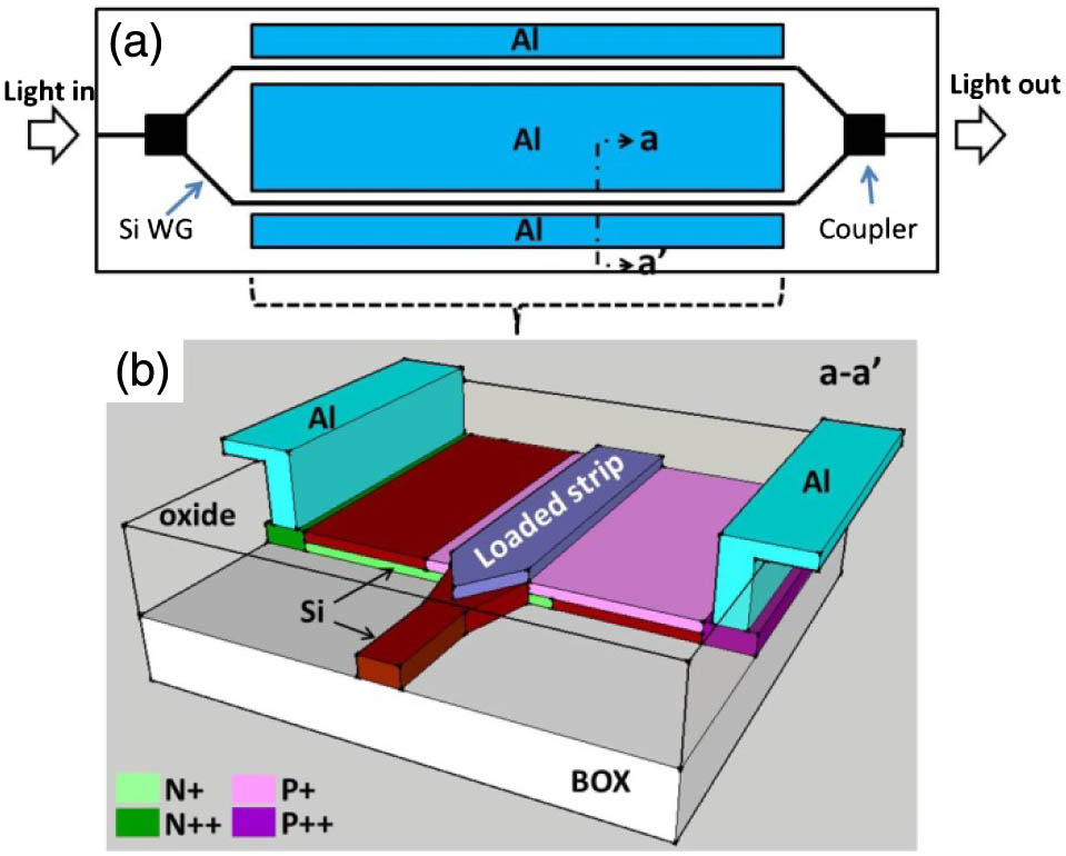
Figure 1.(a) MZM schematic with proposed phase shifters. (b) Proposed phase shifter using heterogeneous strip-loaded waveguide.
Strip-loaded waveguides have various benefits in constructing phase shifters for optical modulators. First of all, they do not require half-etching in waveguide fabrication. In the proposed structure, the SOI layer is not etched because the waveguide is formed by loading a heterogeneous strip and has an etching endpoint layer. Therefore, the strip height can be determined precisely for the whole wafer. On the other hand, in conventional modulators based on half-etched rib waveguides, it is very difficult to precisely control the rib height because the etching endpoint cannot be monitored. In addition, the fluctuation of slab thickness greatly limits the stability and uniformity of silicon modulators produced on a large scale such as a 300 mm line.
Another advantage is precise control of the implantation profile. In the proposed structure, ions can be implanted into the flat SOI wafer before the strip is formed, and any intended dopant profile can be precisely obtained. For example, in a vertical PN junction, where the overlap of the optical field and depletion region, or modulation efficiency, can be significantly increased, an optimal dopant profile can easily be obtained. On the other hand, in the conventional rib waveguide, there are step differences around the rib and slab corners for which optimal doping profiles cannot be obtained simultaneously. In particular, in a phase shifter using vertical PN diodes based on a half-etched rib waveguide, the risk of electrical breakdown at the corners of the waveguide cores increases as the bias voltage increases. If this occurs, the optical modulation disappears at high reverse bias when the depletion region touches the corners, and it is very difficult to construct a vertical PN junction modulator in rib waveguides. Indeed, there are not so many reports of vertical PN junction modulators based on rib waveguides.
A third advantage is ease of design optimization for different purposes. It is well known that a performance tradeoff always exists between efficiency and bandwidth in depletion-type phase shifters. A large overlap between the optical field and depletion region increases modulation efficiency, while the overlap’s large capacitance decreases operation bandwidth. So far, the performance tradeoff for conventional phase shifters is almost always determined by means of trial and error cycles. Optimal device parameters, such as the doping depth, dose, and PN overlap, significantly vary with rib height deviation. For the proposed phase shifter, however, the modulation performance can be stably adjusted by tuning the doping depth, doses, or PN overlap. Accordingly, the rib height issue just described for the conventional phase shifter is resolved.
3. HYDROGENATED AMORPHOUS SILICON STRIP-LOADED MODULATOR
A. Structure
In the proposed structure, it is very important to select an appropriate material for the strip. For high-speed modulators, the strip material should have a large refractive index so that the optical field and PN overlap region is compact. Of course, the strip material should have high optical transmittance. From these viewpoints, a-Si:H is a superior material for the strip, and we have already developed a low-loss a-Si:H wire waveguide that is compatible with silicon photonics processes [20,21]. In addition, a-Si:H has a refractive index as high as 3.5, so it can provide strong optical confinement and contribute to compactness. Figure 2(a) shows a cross-sectional schematic of an a-Si:H strip-loaded phase shifter constructed in a flat SOI structure. A thin thermal oxide layer is inserted between the a-Si:H and SOI layers. The oxide layer is typically 10 nm thick and also works as a passivation layer for the electronic structure. In the SOI layer below the a-Si:H strip, a vertical PN junction is formed for phase modulation. As shown in Fig. 2(b), the optical field in a strip-loaded waveguide constructed with 220 nm thick SOI and 800 nm wide, 75 nm high a-Si:H can be well confined inside the SOI layer. The strip width was determined so that the mode field is minimized. For the fabrication, etching of an a-Si:H strip is easier because the thermal oxidation and ion implantation can be done prior to its deposition. For comparison, a cross-sectional schematic and the optical field of a conventional rib waveguide are shown in Figs. 2(c) and 2(d). The rib width is set to 600 nm, a typical value in this kind of device. From the viewpoint of practical performance, stability and uniformity are the most serious issues in the conventional vertical junction devices. For the comparison, we adopted a conventional lateral junction device, which is widely used as a standard Si optical modulator. In these mode-field calculations, refractive indices of the SOI layer, a-Si:H, and cladding/passivation were set to 3.48, 3.50, and 1.44, respectively.

Figure 2.(a) Cross-sectional schematic of the proposed a-Si:H strip-loaded modulator. (b) Optical field of strip-loaded waveguide for 75 nm thick and 800 nm wide a-Si:H strip. (c) Cross-sectional schematic of a rib waveguide for conventional modulators. (d) Optical field of rib waveguide for 110 nm high and 600 nm wide rib.
Figure 3 shows the optical confinement factor for the core regions in the strip and rib waveguides as a function of strip and rib height. The core regions are defined in Figs. 2(b) and 2(d). As shown in this figure, the sensitivity of the confinement factor to the strip height in the strip-loaded waveguide is almost the same as that to the rib height in the rib waveguide. Since the strip height can be precisely controlled by the etching endpoint layer, the strip-loaded waveguide is advantageous for uniformity of modulation efficiency on a large-scale wafer.
Figure 3.Confinement factors of strip-loaded waveguide and rib waveguide as functions of strip and rib height.
Figure 4 shows the overlap integral of the optical field and depletion region as a function of lateral displacement of the PN junction position. The overlap width of the vertical PN junction was set to 0.6 μm. For simplicity, the thickness of the depletion region was assumed to be 100 nm. As shown in this figure, with the lateral junction displacement of , the overlap integral varies by 16% in the proposed structure while it varies by 50% in the conventional rib waveguide with the lateral PN junction. Thanks to the weak sensitivity of the overlap integral to the lateral displacement of the PN junction, the proposed phase shifter can work with a large allowance for lateral alignment error between the junction and waveguide core, which can easily occur in the photolithography process. This capability overcomes fabrication limitations and eliminates many of the negative factors associated with the conventional rib waveguide.
Figure 4.Overlap integral of optical mode field and depletion region as function of strip and rib height.
B. Modulation Efficiency
We performed device simulations for the proposed phase shifter with a 75 nm high and 800 nm wide strip on 220 nm SOI. We set the doping densities of low-dose and high-dose regions to and , respectively. The high-dose region for electrical contacts was located 1 μm from the waveguide center, so that it would not affect the optical absorption in that region. The PN overlap width is the important parameter with respect to the performance tradeoff between modulation efficiency and speed. For comparison, we also performed a simulation for the conventional lateral PN phase shifter based on a half-etched rib waveguide. The SOI thickness, rib height, and rib width were 220, 110, and 600 nm, respectively.
Normally, the modulation efficiency of phase shifters is described by , which denotes the multiplication of the -shift voltage and device length. Small means high efficiency. Figure 5(a) shows the phase shift in relation to the bias voltage for a device length of 5 mm and DC bias references. For the proposed phase shifter, the PN overlap width is tuned from 0.6 to 0.9 μm. The -shift voltages () are 2.0 and 3.2 V for the proposed structure with a 0.6 μm overlap and a conventional structure, respectively. The corresponding values of , the figure of merit used to describe the modulation efficiency, are 1.0 and 1.6 V·cm. This indicates efficiency enhancement of times in the proposed phase shifter. Figure 5(b) shows the dependence of the modulation efficiency on the PN overlap width. Further increasing the PN overlap can continue to enhance the efficiency, which increases from 1.0 to 0.89 V·cm. The with a change in the PN overlap can be interpreted as stability, or robustness. The efficiency fluctuation, 0.11 V·cm, is small enough within the 300 nm overlap variance. Therefore, the modulation efficiency is acceptable because the alignment accuracy of the photolithography related to ion implantation is not more than 100 nm.
Figure 5.(a) Phase shift in relation to reverse bias. (b) PN overlap dependence of efficiency .
C. Propagation Loss
Figure 6 compares the bias voltage dependence of the propagation loss for the conventional lateral PN phase shifter and the proposed phase shifter with three different overlap widths. The total propagation loss of the proposed phase shifter is much lower than that of the conventional one. For example, at bias, the propagation loss can be significantly reduced from 24 to 17 dB/cm. There is little change in the propagation loss due to variation of the PN overlap. In particular, that for all PN overlaps corresponds to around , which is usually set as the operation bias. Therefore, stabilized propagation loss is achieved within the alignment accuracy of photolithography. The propagation loss reduction in the proposed structure is mainly due to a large overlap between the optical field and depletion region, where carrier plasma absorption is lower than in other P and N regions. Further increasing the PN overlap with the depletion layer will further reduce propagation loss.
Sign up for Photonics Research TOC. Get the latest issue of Photonics Research delivered right to you!Sign up now
Figure 6.Comparison of propagation loss between the conventional lateral PN modulator in the rib waveguide and the proposed vertical one with three different overlap distances.
D. Transient and Frequency Response
The intrinsic modulation speed of a phase shifter is governed by the resistor–capacitor (RC) time constant. Figure 7 compares the voltage dependence of capacitance for the conventional lateral PN phase shifter and the proposed vertical PN shifter with 0.6 μm overlap. The respective calculated capacitances for the conventional structure and proposed one are 0.30 and 0.79 fF/μm at around , which is the typical operation bias. The calculated resistances are 2.88 and 1.94 Ω; thus, the intrinsic modulation speeds are estimated to be 36.7 and 20.8 GHz for the conventional structure and proposed one, respectively. The speed of the conventional structure is higher than that of the proposed one because the overlap between the optical field and depletion region in the conventional structure is small. However, the design and resultant electrical performance of the electrodes can significantly influence the high-frequency performance of a modulator. Therefore, there might not be such a large difference in the practical modulation speed between the conventional structure and the proposed one.
Figure 7.Capacitance of the conventional lateral PN junction and the proposed vertical one as a function of bias.
In the proposed structure with 0.6 μm overlap, the transient phase-shift response was calculated under a 2 V step pulse condition with 10 ps duration. As shown in Fig. 8(a), almost a 1 phase change was obtained for a 2 V voltage difference. If considering a push–pull driving method for an arm-balanced Mach–Zehnder configuration, only 1 V is required for half- driving. To obtain the response time, an exponential decay fitting to the phase response was performed, which indicated a time constant of 20 ps. The electro-optic (E–O) response calculated from the impulse response is shown in Fig. 8(b), which reveals a 3 dB bandwidth of . Therefore, this response approximately corresponds to the intrinsic modulation speed calculated previously.
Figure 8.(a) Transient response and (b) frequency response of the proposed phase shifter.
4. CONCLUSION
We propose a novel silicon optical phase shifter based on strip-loaded waveguides on a photonic SOI platform. An etchless SOI layer, with a vertical PN diode structure, and a strip-loaded waveguide can enhance both the performance and uniformity of silicon modulators on a large-scale wafer. We performed device simulation of a phase shifter with an a-Si:H strip loaded onto the SOI layer. Compared to conventional lateral PN phase shifters based on half-etched rib waveguides, this phase shifter achieves 1.6 times higher modulation efficiency enhancement and propagation loss reduction at around the typical operation bias. Both the efficiency improvement and propagation loss reduction are a result of the increase in the PN overlap between the optical field and depletion region. In spite of the enhanced modulation efficiency, the proposed phase shifter provides a frequency response of over 20 GHz, and it will have various beneficial uses such as in state-of-the-art 28 Gbps quadrature phase-shift keying applications.
References
[1] L. Liao, A. Liu, D. Rubin, J. Basak, Y. Chetrit, H. Nguyen, R. Cohen, N. Izhaky, M. Paniccia. 40 Gbit/s silicon optical modulator for high-speed applications. Electron. Lett., 43, 1196-1197(2007).
[2] J. Fujikata, S. Takahashi, M. Takahashi, M. Noguchi, T. Nakamura, Y. Arakawa. High-performance MOS-capacitor-type Si optical modulator and surface-illumination-type Ge photodetector for optical interconnection. Jpn. J. Appl. Phys, 55, 04EC01(2016).
[3] F. Gan, F. X. Kärtner. High-speed silicon electrooptic modulator design. IEEE Photon. Technol. Lett., 17, 1007-1009(2005).
[4] G.-R. Zhou, M. W. Geis, S. J. Spector, F. Gan, M. E. Grein, R. T. Schulein, J. S. Orcutt, J. U. Yoon, D. M. Lennon, T. M. Lyszczarz, E. P. Ippen, F. X. Kärtner. Effect of carrier lifetime on forward-biased silicon Mach-Zehnder modulators. Opt. Express, 16, 5218-5226(2008).
[5] S. Akiyama, T. Baba, M. Imai, T. Akagawa, M. Takahashi, N. Hirayama, H. Takahashi, Y. Noguchi, H. Okayama, T. Horikawa, T. Usuki. 12.5-Gb/s operation with 0.29-V·cm VπL using silicon Mach-Zehnder modulator based-on forward-biased pin diode. Opt. Express, 20, 2911-2923(2012).
[6] M. R. Watts, W. A. Zortman, D. C. Trotter, R. W. Young, A. L. Lentine. Low-voltage, compact, depletion-mode, silicon Mach-Zehnder modulator. IEEE J. Sel. Top. Quantum Electron., 16, 159-164(2010).
[7] D. Marris-Morini, L. Vivien, J. M. Fédéli, E. Cassan, P. Lyan, S. Laval. Low loss and high speed silicon optical modulator based on a lateral carrier depletion structure. Opt. Express, 16, 334-339(2008).
[8] N. N. Feng, S. Liao, D. Feng, P. Dong, D. Zheng, H. Liang, R. Shafiiha, G. Li, J. E. Cunningham, A. V. Krishnamoorthy, M. Asghari. High speed carrier-depletion modulators with 1.4 V-cm VπL integrated on 0.25 μm silicon-on-insulator waveguides. Opt. Express, 18, 7994-7999(2010).
[9] K. Ogawa, K. Goi, Y. T. Tan, T.-Y. Liow, X. Tu, Q. Fang, G.-Q. Lo, D.-L. Kwong. Silicon Mach-Zehnder modulator of extinction ratio beyond 10 dB at 10.0–12.5 Gbps. Opt. Express, 19, B26-B31(2011).
[10] G. Kim, J. W. Park, I. G. Kim, S. Kim, S. Kim, J. M. Lee, G. S. Park, J. Joo, K. S. Jang, J. H. Oh, S. A. Kim, J. H. Kim, J. Y. Lee, J. M. Park, D. W. Kim, D. K. Jeong, M. S. Hwang, J. K. Kim, K. S. Park, H. K. Chi, H. C. Kim, D. W. Kim, M. H. Cho. Low-voltage high-performance silicon photonic devices and photonic integrated circuits operating up to 30 Gb/s. Opt. Express, 19, 26936-26947(2011).
[11] T. Baehr-Jones, R. Ding, Y. Liu, A. Ayazi, T. Pinguet, N. C. Harris, M. Streshinsky, P. Lee, Y. Zhang, A. E.-J. Lim, T.-Y. Liow, S. H.-G. Teo, G.-Q. Lo, M. Hochberg. Ultralow drive voltage silicon traveling-wave modulator. Opt. Express, 20, 12014-12020(2012).
[12] K. Goi, K. Oda, H. Kusaka, Y. Terada, K. Ogawa, T.-Y. Liow, X. Tu, G.-Q. Lo, D.-L. Kwong. 11-Gb/s 80-km transmission performance of zero-chirp silicon Mach-Zehnder modulator. Opt. Express, 20, B350-B356(2012).
[13] D. Petousi, L. Zimmermann, K. Voigt, K. Petermann. Performance limits of depletion-type silicon Mach–Zehnder modulators for telecom applications. J. Lightwave Technol., 31, 3556-3562(2013).
[14] H. Xu, X. Xiao, X. Li, Y. Hu, Z. Li, T. Chu, Y. Yu, J. Yu. High speed silicon Mach-Zehnder modulator based on interleaved PN junctions. Opt. Express, 20, 15093-15099(2012).
[15] H. Yu, M. Pantouvaki, J. V. Campenhout, D. Korn, K. Komorowska, P. Dumon, Y. Li, P. Verheyen, P. Absil, L. Alloatti, D. Hillerkuss, J. Leuthold, R. Baets, W. Bogaerts. Performance tradeoff between lateral and interdigitated doping patterns for high speed carrier-depletion based silicon modulators. Opt. Express, 20, 12926-12938(2012).
[16] G. T. Reed, G. Z. Mashanovich, F. Y. Gardes, M. Nedeljkovic, Y. Hu, D. J. Thomson, K. Li, P. R. Wilson, S.-W. Chen, S. S. Hsu. Recent breakthroughs in carrier depletion based silicon optical modulators. Nanophotonics, 3, 229-245(2014).
[17] .
[18] Lumerical Solutions,.
[19] Lumerical Solutions,.
[20] K. Furuya, K. Nakanishi, R. Takei, E. Omoda, M. Suzuki, M. Okano, T. Kamei, M. Mori, Y. Sakakibara. Nanometer-scale thickness control of amorphous silicon using isotropic wet-etching and low loss wire waveguide fabrication with the etched material. Appl. Phys. Lett., 100, 251108(2012).
[21] R. Takei, S. Manako, E. Omoda, Y. Sakakibara, M. Mori, T. Kame. Sub-1 dB/cm submicrometer-scale amorphous silicon waveguide for backend on-chip optical interconnect. Opt. Express, 22, 4779-4788(2014).


