Hongtao Lin, Boshu Sun, Hui Ma, Chuyu Zhong, Zezhao Ju. Review of mid-infrared on-chip integrated photonics (Invited)[J]. Infrared and Laser Engineering, 2022, 51(1): 20211111
Search by keywords or author
- Infrared and Laser Engineering
- Vol. 51, Issue 1, 20211111 (2022)
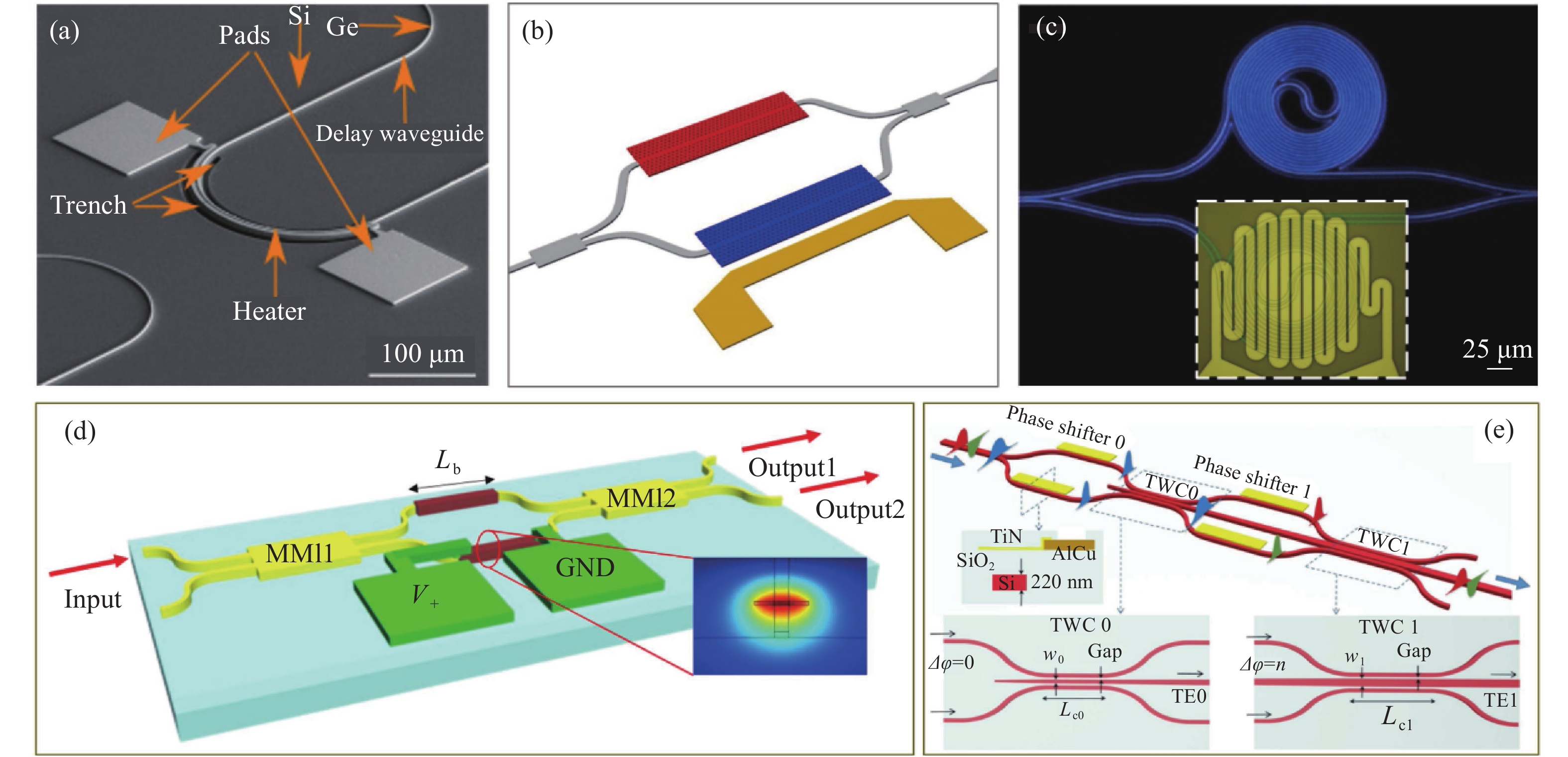
![(a) Thermo-optical (TO) modulator based on Ge-on-SOI waveguide platform [6]; (b) Si-on-sapphire TO modulator with PhC (photonic crystal) waveguide[7]; (c) TO modulator based on SOI with spiral waveguides arms. Inset shows the heater [8]; (d) 2×2 MZI TO switch[10]and; (e) Dual mode TO switch based on SOI MZI structure at 2 μm band[11]](/richHtml/irla/2022/51/1/20211111/img_1.jpg)
Fig. 1. (a) Thermo-optical (TO) modulator based on Ge-on-SOI waveguide platform [6]; (b) Si-on-sapphire TO modulator with PhC (photonic crystal) waveguide[7]; (c) TO modulator based on SOI with spiral waveguides arms. Inset shows the heater [8]; (d) 2×2 MZI TO switch[10]and; (e) Dual mode TO switch based on SOI MZI structure at 2 μm band[11]
![Thermo-optic modulator with doped-silicon heater[12]. (a) Microscope image, (b) the static response and (c) the dynamic response of the MZI modulator; (d) Microscope image, (e) the static response and (f) the dynamic response of the MRR-based modulator](/richHtml/irla/2022/51/1/20211111/img_2.jpg)
Fig. 2. Thermo-optic modulator with doped-silicon heater[12]. (a) Microscope image, (b) the static response and (c) the dynamic response of the MZI modulator; (d) Microscope image, (e) the static response and (f) the dynamic response of the MRR-based modulator
Fig. 3. (a) Diagrams of silicon photonic circuits integrated with LiNbO3 thin plate, wafer, single die and basic circuit and the cross-section illustration of bonding[16]; (b) Integrated Ta2O5 -LiNbO3 rib waveguide[17]; (c) Mid-infrared electro-optic modulator based on Si-on-LiNbO3 waveguide[18]
Fig. 4. Changes of (a) refractive index and (b) absorption coefficient of silicon and germanium in the Mid--IR caused by free carrier; (c) Wavelength scaling of −Δn /Δk [23], the carrier concentration is fixed at 5×1017 cm−3
Fig. 5. (a), (b) carrier-injection modulators[24,26] and (c) carrier-depletion modulators based on SOI [27]; (d) Electro-optic modulator and electro-absorption modulator on Ge-on-Si [28]
Fig. 6. Graphene-chalcogenide modulator[4]. (a) The structure and working principle of the graphene Mid-IR waveguide modulator; (b) Measured and (c) simulated modulation depth of the device versus wavelength and bias (Unit: dB/mm)
Fig. 7. Performance of Mid-IR graphene-chalcogenide modulators[38]. (a) The Fermi-level-related optical absorption of a graphene layer across the Mid-IR band evaluated by the surface conductive model; (b) Simulation result of modulation depth for graphene mid-IR electro-absorption modulators (The white dashed line is zero modulation depth); (c) FOM (modulation depth/insertion loss) of the modulator (The black dashed line represents unity FOM)
Fig. 8. Mid-IR extrinsic silicon photodetectors. (a) B doped SOI detector; (b) SEM of the same device (Inset: Schematic diagram of a silicon waveguide); (c) Relationship between the reverse bias voltage and the photocurrent/response of the detectorat two micron wavelength range; (d) Eye diagram of the detector with voltage of 27 V[56, 69]
Fig. 9. Mid-infrared Black Phosphorus(BP) detector. (a)-(b) Structure of the silicon-based BP slow-light integrated detector; (c) Relationship between the power and the responsivity of the BP detector at three different wavelengths; (d) Current noise power density of the photonic crystal waveguide and the subwavelength grating waveguide BP photodetectors, respectively[52]
| ||||||||||||||||||||||||||||||||||||||||||||||||||||||||||||||||||||||||||||||||||||||||||||||||||
Table 1. Hybrid integrated photodetectors with different active materials on silicon

Set citation alerts for the article
Please enter your email address


