Qiang Zhang, Ning Jiang, Yiqun Zhang, Anran Li, Huanhuan Xiong, Gang Hu, Yongsheng Cao, Kun Qiu, "On-chip spiking neural networks based on add-drop ring microresonators and electrically reconfigurable phase-change material photonic switches," Photonics Res. 12, 755 (2024)
Copy Citation Text
【AIGC One Sentence Reading】:We propose a photonic spiking neural network using ring microresonators and phase-change material switches, demonstrating handwritten digit recognition, paving the way for efficient neuromorphic photonic systems.
【AIGC Short Abstract】:We introduced a photonic spiking neural network using add-drop ring microresonators and phase-change material switches. This neuromorphic system demonstrates dual neural dynamics and can generate optical neural spikes. A thermodynamic leaky integrate-and-fire neuron system was proposed, enabling a fully connected spiking neural network for deep learning tasks like handwritten digit recognition. Simulation results show effective optical recognition using the surrogate gradient algorithm, opening new possibilities for efficient neuromorphic photonic systems.
Note: This section is automatically generated by AI . The website and platform operators shall not be liable for any commercial or legal consequences arising from your use of AI generated content on this website. Please be aware of this.
Abstract
We propose and numerically demonstrate a photonic computing primitive designed for integrated spiking neural networks (SNNs) based on add-drop ring microresonators (ADRMRs) and electrically reconfigurable phase-change material (PCM) photonic switches. In this neuromorphic system, the passive silicon-based ADRMR, equipped with a power-tunable auxiliary light, effectively demonstrates nonlinearity-induced dual neural dynamics encompassing spiking response and synaptic plasticity that can generate single-wavelength optical neural spikes with synaptic weight. By cascading these ADRMRs with different resonant wavelengths, weighted multiple-wavelength spikes can be feasibly output from the ADRMR-based hardware arrays when external wavelength-addressable optical pulses are injected; subsequently, the cumulative power of these weighted output spikes is utilized to ascertain the activation status of the reconfigurable PCM photonic switches. Moreover, the reconfigurable mechanism driving the interconversion of the PCMs between the resonant-bonded crystalline states and the covalent-bonded amorphous states is achieved through precise thermal modulation. Drawing from the thermal properties, an innovative thermodynamic leaky integrate-and-firing (TLIF) neuron system is proposed. With the TLIF neuron system as the fundamental unit, a fully connected SNN is constructed to complete a classic deep learning task: the recognition of handwritten digit patterns. The simulation results reveal that the exemplary SNN can effectively recognize 10 numbers directly in the optical domain by employing the surrogate gradient algorithm. The theoretical verification of our architecture paves a whole new path for integrated photonic SNNs, with the potential to advance the field of neuromorphic photonic systems and enable more efficient spiking information processing.
1. INTRODUCTION
The emergence of artificial intelligence (AI) technology has revolutionized various aspects of human society, showcasing remarkable accomplishments in cognitive tasks such as image recognition [1] and natural language processing (NLP) [2]. However, the performance of extensive parallel computing tasks using conventional von Neumann architectures [3] results in considerable processing latency and power inefficiency, which contrasts with the highly efficient massively parallel processing capabilities of the brain. Recently, brain-inspired neuromorphic systems have attracted significant attention as promising approaches to enhance parallel computing efficiency and enable in-memory computing capabilities [4–10]. Among diverse neuromorphic networks, SNNs, commonly recognized as the third generation of neural networks, closely emulate the architecture and functionality of the biological brain, demonstrating greater biological plausibility and energy efficiency [11–16]. Recently, noteworthy advancements have been made in the electronic hardware implementation of several SNNs, with notable examples including SpiNNaker [17], Neurogrid [18], TrueNorth [19], and Tianjic [20]. However, prevalent electronic neuromorphic systems predominantly adopt a shared digital communications bus through time division multiplexing (TDM) for AI matrix computations. This TDM-based compromise between interconnectivity and bandwidth imposes multiple restrictions concerning low bandwidth efficiency, limited parallelism, and large processing latency. In contrast, photonic counterparts can fully harness the potential of wavelength division multiplexing (WDM) technology, coupled with their exceptionally high bandwidth, minimal energy consumption, and negligible electromagnetic interference, to perform highly efficient massively parallel matrix operations in photonic networks [21]. These unique capabilities significantly boost the performance of neuromorphic computing. Therefore, the implementation of SNNs through photonic hardware presents a promising avenue to achieve ultrafast neuromorphic computing.
In recent years, significant progress has been made in the design of optical devices with the capability to mimic spiking neurons and synapses, facilitating the development of photonic SNNs [22–35]. As an illustration, vertical-cavity surface-emitting lasers (VCSELs), which effectively mimic biologically plausible nonlinear spiking responses, have established themselves as pivotal active devices in the field of photonic neuromorphic computing. Their noteworthy accomplishments encompass the successful implementation of a variety of VCSEL-based SNNs, which demonstrate the capability to handle various neuromorphic computing tasks [36–45]. In addition to their active counterparts, passive optical devices possess immense potential for realizing photonic SNNs with large-scale integration and ultralow power consumption. For instance, passive chalcogenide PCMs, such as (GST), have been demonstrated as functional blocks in in-memory computing platforms, showcasing the advantages of reversible phase transition, high scalability, and low power consumption. Utilizing GST-on-silicon waveguides, significant research efforts have been devoted to the development of CMOS-compatible, compact, and reconfigurable photonic switching units [46–59]. These inherently nonvolatile switches are characterized by near-zero static loss and outstanding durability in reversible switching, making them ideally suited for passive neuromorphic systems. Moreover, in 2019, Feldmann et al. proposed an all-optical spiking neurosynaptic network and showcased its ability to perform the fundamental task of pattern recognition, emphasizing the scalability of photonic SNNs and their remarkably low static power consumption [32]. Concurrently, Chakraborty et al. proposed an innovative photonic computing primitive based on a nonvolatile synaptic array and bipolar integration-firing neurons, enabling the potential for massively integrated in-memory computing as well as ultrafast neuromorphic computation [60,61]. In 2020 and 2022, Xiang et al. theoretically and experimentally presented an all-optical spiking neuron based on passive microresonators [62,63]. Subsequently, our previous work demonstrated an all-optical synaptic neuron based on add-drop microring resonators with power-tunable auxiliary light, highlighting the capability of passive add-drop microring resonators for dual neural dynamics, encompassing spiking response and synaptic plasticity [64]. By cascading these microring-based synaptic neurons and combining with a PCM switch, an LIF neuron that supports flexible implementation of a synaptic weighting operation and layer-individual spike generation can be achieved [65]. Nevertheless, compared to the advancements made in SNNs based on active optical devices, passive approaches are still in their infancy. An inherent challenge lies in the absence of optical excitation in passive devices, making the realization of spiking neurons using passive components considerably more formidable than with active devices. Thus, research in the passive domain is particularly scarce. Moreover, within the framework of WDM-based SNNs, the structural paradigm to simultaneously achieve both a spiking response and synaptic plasticity at a single wavelength within a single device has been largely disregarded for an extended period. However, such devices and models that enable dual neural dynamics have the capacity to maximize device utilization. Additionally, in passive GST-based photonic switches, the manual transmission of reset pulses after each activation, required to restore GST to its initial state, imposes constraints on achieving large-scale integration within GST-based passive SNNs.
In this paper, we propose an on-chip SNN based on ADRMRs and electrically reconfigurable PCM photonic switches. In this neuromorphic system, a hardware matrix array is constructed by cascading the silicon-on-insulator (SOI) ADRMRs with distinct resonant wavelengths. It is demonstrated that each ADRMR within the ADRMR-based array can serve as a synaptic neuron based on its nonlinearity-induced self-pulsation, excitability, and synaptic plasticity. When external wavelength-addressable optical pulses are injected, they trigger the nonlinear effects of the ADRMRs corresponding to the respective wavelengths within the ADRMR-based array. As a result, multiwavelength weighted spikes are generated at the terminal of the ADRMR-based array. Then, the output multiwavelength weighted spikes are converted into electrical power input to the positive electrode of the electrically reconfigurable GST optical switch via a photodetector (PD). Activation of the electrically reconfigurable GST optical switch takes place when the accumulated Joule heat, resulting from the TLIF dynamics impact of multiwavelength weighted spikes on the heater of the switch, reaches the GST melting point. The activation status of the GST switch is continuously monitored in real-time by employing a continuous beam of light; then, an automatic output spike and reset operation are executed upon switch activation. Finally, an exemplary four-layer fully-connected SNN is formed by integrating the ADRMR-based arrays and electronically reconfigurable GST photonic switches. The exhibited capabilities of this proposed SNN in successfully accomplishing image recognition tasks are explicitly highlighted through its recognition of datasets, including MNIST and EMNIST.
Sign up for Photonics Research TOC. Get the latest issue of Photonics Research delivered right to you!Sign up now
2. PRINCIPLE
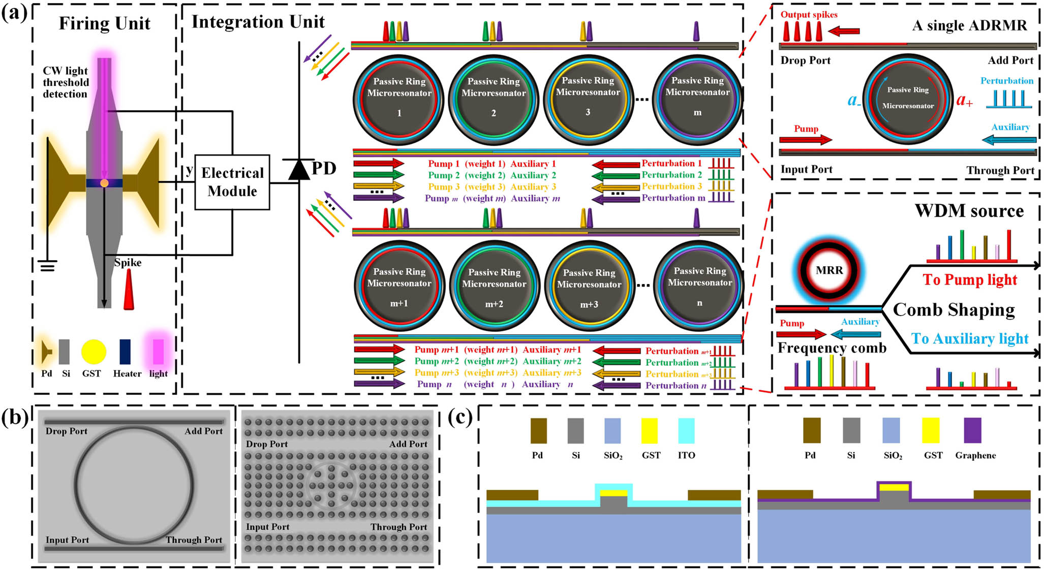
Figure 1(a) presents the schematic of our proposed TLIF neuron system, which mainly incorporates an integration unit and a firing unit. The integration unit of the TLIF neuron system comprises an ADRMR-based synaptic neuron array, a PD, a WDM source, and an electronic module; the firing unit consists of an electrically reconfigurable GST photonic switch, a beam of probe continuous light, and an output neural spike. In the integration unit, an on-chip optical frequency comb is generated as the WDM source for the ADRMR array, via an auxiliary laser heating approach [66,67]. The WDM source is split into two components, with each part being directed into the “input” port (pump light) and the “through” port (auxiliary light) of the cascaded ADRMRs, respectively. The resonant wavelengths of ADRMRs are set to correspondingly match with the wavelengths of the WDM source. Next, our attention will be directed toward the ADRMR, one of the essential foundational components in the proposed TLIF neuron system. Figure 1(b) illustrates the two silicon-based ADRMRs: an add-drop microring resonator [68] and a photonic crystal add-drop ring resonator [69,70]. In such a scenario, by accurately tuning the powers of the pump and auxiliary light above a certain threshold, along with appropriate wavelength detuning, self-pulsation would be observed in ADRMRs. Then, by decreasing the sum power of both the pump light and the auxiliary light below the self-pulsation threshold power, the ADRMRs would be excited to output neural spikes through adding perturbations of proper strength to the auxiliary light. Moreover, by injecting two beams of power-tunable and opposite-direction continuous light into the ADRMRs and maintaining their sum power at a constant value, linearly-tunable and single-wavelength neural spikes can be generated in virtue of the nonlinear effects triggered by perturbation pulses. Utilizing coupled mode theory (CMT) for the passive side-coupled microresonator, a universal synaptic neuron model applicable to all silicon-based ADRMRs with a power-tunable auxiliary light to describe these nonlinear effects, can be expressed through [62,64,71–76] Within these equations, the symbols “+” and “−” signify the forward and backward directions, respectively. Here, represents the complex amplitude of the propagation mode, and stands for the density of free carriers in the ADRMR. Additionally, () is the complex amplitude of pump (auxiliary) light, while represents the complex amplitude of the perturbation light. Furthermore, indicates the complex amplitude of the output light at the “drop” port. Several other key parameters are involved: the cold resonance frequency , the nonlinear frequency shift , the frequency of the input light in the waveguide , the mode-averaged temperature difference with the environment , the relaxation time for temperature , the effective free-carrier decay rate , the density of silicon , the thermal capacity of silicon , the effective mode volume , the confinement coefficient , the propagation constant in the output waveguide , the finite distance between the reference planes , the absorption power , the coupling coefficient , the constant governing two-photon absorption , the velocity of light , the group index , the correction factor taking values in the range 1–2, and the total loss for the cavity mode .
Figure 1.Core structure of the proposed on-chip silicon-based computational primitive. (a) Schematic representation of the TLIF neuron system, comprising an ADRMR-based synaptic neuron array, a photodetector (PD), an electronic module, a WDM optical source, a beam of probe continuous light, an output neural spike, and an electrically reconfigurable GST photonic switch. Real-time multiwavelength weighted spikes generated by the ADRMR-based synaptic neuron array are guided into the PD and then enter the electrical module for processing. Activation of the electrically reconfigurable GST photonic switch occurs upon reaching a predefined threshold of cumulative power from the weighted spikes. This activation leads to the continuous detection of light at the switch output, subsequently triggering an output neural spike and a reset pulse. (b) Two types of ADRMRs: add-drop microring resonator and photonic crystal add-drop ring resonator. (c) Electrically reconfigurable GST photonic switches with an ITO heater and a graphene heater, respectively.
Next, in the scenario of multiple parallel-connected synaptic neurons based on ADRMRs, each characterized by distinct resonant wavelengths, their individual output spikes are coupled into a single waveguide. The cumulative power of these multiwavelength weighted spikes is calculated as where represents the complex amplitude of light emitted from the th ADRMR at the “drop” port at time . The value of depends on the number of ADRMR-based neurons in the array.
Next, the output spikes generated by the hardware array consisting of ADRMRs are directed toward an integrated PD. The PD executes the transformation of these optical spikes into electrical spikes, which are then transmitted to the electronic module for further processing. The electronic module primarily handles biasing and amplification operations on the electrical spikes converted by the PD, concomitantly establishing a linear correlation between optical power and electrical power, ultimately culminating in the generation of a total power density that can be calculated by where denotes the responsivity of the photodetector, represents the bias current, and the current amplification is indicated by . To enhance the flexibility of the overall SNNs, the value can be dynamically modulated.
Finally, the cumulative weighted electronic spikes are directed to the firing unit. The pivotal component within the firing unit is an electrically reconfigurable GST photonic switch. Within Fig. 1(c), two representative electrically reconfigurable GST photonic switches are depicted, employing indium tin oxide (ITO) and graphene as electrical heaters. Here, a concise overview of the optical properties of the electrically reconfigurable GST optical switches is given. In the context of programmable photonic applications, strong optical modulation and low insertion loss are essential for the optimal optical performance of the GST optical switch. It is demonstrated that these GST-based optical switches exhibit notable contrasts in resistivity and complex refractive indices across a wide spectral range when undergoing a structural phase transition from the covalent-bonded amorphous form to the resonant-bonded crystalline state. In its crystalline state, GST displays an elevated refractive index and extinction coefficient values, resulting in a significantly reduced optical transmission capability of the device. In contrast, the transition of GST from its crystalline state to a disordered glassy state, accompanied by lower optical constants, enhances the optical transmission properties of the device. To elucidate the optical properties of the electrically reconfigurable GST optical switches more effectively, the mode profiles of the photonic switching units were modeled and simulated using a frequency-domain two-dimensional (2D) finite element method (FEM), achieved through mode analysis. Then, in terms of the reconfigurable mechanism, electrically reconfigurable GST photonic switches employ external heaters to achieve electrical switching. This process relies on the transmission of joule heat, generated by electrical pulses from the heaters, to induce status transitions in the GST. Therefore, nonlinear threshold activation is accomplished when the cumulative power of weighted output spikes stemming from the ADRMR-based array reaches a threshold that generates joule heat adequate to induce the transition of the GST photonic switch from the crystalline state to the disordered glass state. Subsequently, the GST material was heated to a level slightly above its glass transition temperature yet remained below its melting point by employing a low-power and prolonged pulse to promote the nucleation of small crystals and their subsequent growth, resulting in a return to the crystalline state of high optical constants. Additionally, it is crucial to recognize that the heat generated by electrically reconfigurable GST photonic switches may influence other components within the proposed architecture. Therefore, a prudent approach involves the application of thermal isolation measures to adequately segregate arrays of electrically reconfigurable GST photonic switches. To investigate the thermodynamic processes associated with these GST-based optical switches, a coupled electro-thermal 2D FEM model was developed. This model is instrumental in qualitatively simulating the electrical switching of the photonic devices with electronic heaters, enabling the prediction of temperature distributions across the entire switching units. Moreover, in cyclic reconfigurable processes that incorporate GST-based optical switches, the neuron-like dynamics of the system, based on the heat transfer equation, can be elucidated as Here, is the material density, is the thermal conductivity, is the specific heat, and the represents the heating source. The parameter denotes a relatively refractory period. stands for the resting temperature. represents the threshold values for the TLIF neuron system, with the melting point () serving as the threshold for GST. Nevertheless, the coupled electro-thermal 2D FEM model based on the heat transfer equation, although capable of accurate simulation of thermal dynamics, is relatively difficult to utilize to currently complete the calculation of the network. We consider a specific set of cases in the overall TLIF system, where a temperature control circuit is used to maintain the temperature around the switch at a constant value, designated as . The model prescribes the constant temperature as a boundary condition. In this situation, the 2D FEM model based on the heat conduction equation is approximated by the linear differential equation [77] The parameter denotes the heat transfer coefficient, which is utilized to approximate the rate of temperature cooling for fitting the temperature distributions of our proposed 2D FEM model. This linear differential equation represents a typical mathematical model utilized to emulate the most basic LIF neurons. Consequently, these TLIF neuron systems effectively emulate the LIF behavior observed in biological neurons and can be utilized to construct a variety of LIF-based architectures for SNNs.
3. RESULTS AND DISCUSSION
A. Dual Neural Dynamics of the Passive ADRMR
Figure 2(a) presents the schematic of an all-optical synaptic neuron based on ADRMR with a power-tunable auxiliary light. On the one hand, the ADRMR exhibits the capability to generate neural spiking responses akin to those observed in biological neurons when influenced by external stimuli. On the other hand, it governs the output magnitude of the spikes directed to subsequent neurons, in a manner reminiscent of biological synapses. This dual neural dynamic has been demonstrated in an add-drop microring resonator [64]. It is worth underscoring that the add-drop microrings should be considered as a specific case, and the exploration of other ring resonators with dual neural dynamics, including an add-drop microdisk and photonic crystal add-drop ring resonators, is still relatively scarce. Previous reports have introduced a universal CMT for all passive side-coupled microresonators [62,63], providing a structured framework for elucidating the nonlinear-induced self-pulsation and excitability behaviors experimentally observed in these resonators [72,73,78–84]. Here, we narrow down our study to a particular subset of all passive side-coupled microresonators that target ring resonators coupled with two waveguides. Figures 2(b)–2(d) demonstrate the nonlinearity-induced self-pulsation, excitability, and synaptic plasticity behaviors of an add-drop microdisk, an add-drop microring, and a photonic crystal add-drop ring resonator, respectively. In our simulations, the parameter values for the microdisk, microring, and photonic crystal are selected based on reference to previously reported values [62,64,71–75,79,82,84]. Simulation outcomes reveal that all passive ADRMRs, including add-drop microdisks, add-drop microrings, and photonic crystal add-drop ring resonators that meet certain parametric criteria can exhibit self-pulsation behavior upon surpassing a nonlinearity-correlated power threshold. When the input power is decreased below the self-pulsation threshold power, the self-pulsation behavior disappears, and subsequently, a neuron-like excitability of the spiking response can be induced through the activation of the nonlinearity-based self-pulsation using an external perturbation pulse as a power medium. At the same time, the input continuous light, which includes both pump light and auxiliary light and is coupled into the ADRMR from the opposite direction, maintains a constant power. By modulating the power ratio between pump light and auxiliary light, it becomes feasible to generate amplitude-adjustable neural spikes at the “drop” port, and these spikes exhibit an approximately linear variation concerning the power of the pump light. It is noteworthy that ADRMR-based spiking neurons are minimally affected by the shape and noise of the perturbation pulses, and their output spikes exhibit considerable robustness [64]. By controlling the output spike amplitude with our proposed linear scheme, the output spikes also have equal linear changes in energy. Hence, the precise energy-controlled mechanism and robust characteristics of neural spikes contribute to the enhanced accuracy of the proposed neuromorphic computation. Moreover, by capitalizing on the wavelength selectivity and the dual neural dynamics inherent in ADRMRs, the incorporation of ADRMRs with varied wavelengths can be employed to construct arrays conducive to WDM. External wavelength-addressable perturbation pulses with different wavelengths are introduced into the ADRMRs array, and these perturbation pulses seek out the ADRMRs within the array that corresponds to their individual resonant wavelength. Subsequently, the ADRMR-based array responds to these perturbations, generating multiwavelength weighted neural spikes. Furthermore, the photonic crystal-based synaptic neuron can operate much faster than the microdisk- and microring-based synaptic neuron. This accelerated performance imparts heightened computational processing potential to SNNs grounded in photonic crystal-based synaptic neurons.
Figure 2.(a) All-optical ADRMR-based synaptic neuron. (b)–(d) Self-pulsation behavior, excitability behavior, and synaptic plasticity of (from left to right) (b) the microdisk, (c) the add-drop microring, and (d) the photonic crystal add-drop ring resonator.
Subsequently, the compatibility of ADRMR-based synaptic neurons with GST materials was investigated. Regarding the phase change material GST, the transition from the crystalline state to the amorphous state is achieved using high-power, short-duration energy pulses. These pulses rapidly elevate the temperature of GST above its melting point, leading to the fracture of chemical bonds associated with the resonance-bonded crystalline state and the transformation into the covalent-bonded amorphous state [85]. Our simulation results indicate that the output spike durations generated by the add-drop microdisk, add-drop microrings, and photonic crystal add-drop ring resonators are approximately 150 ns, 25 ns, and 10 ns, respectively. The nanosecond-duration pulses generated by these ADRMRs can be employed to induce the transition of GST from the crystalline to the amorphous state. As shown in Figs. 3(a1), 3(b1), and 3(c1), the amplified output spikes of microring-based synaptic neurons and photonic crystal-based synaptic neurons are inputted into the electrically reconfigurable GST photonic switching models with an ITO heater and a graphene heater, respectively. The real-time temperature distribution () of the GST optical switches was obtained in response to this specific form of electrical pulse. Here, it is hypothesized that the phase transitions are smoothly undergone within a limited temperature interval of (), centered around () for the purpose of swift melting (and relatively slow crystallization) [52,53]. The simulation parameters for the electrically reconfigurable GST photonic switches were adopted from previously reported literature [47,52,53,86–88]. Figure 3(a1) illustrates that when the pulse power remains below a certain threshold, the joule heat produced by the ITO heater does not attain the required level to reach the melting point (). Consequently, the GST does not undergo a transition into a disordered glassy state. However, Figs. 3(b1) and 3(c1) showcase that upon reaching a specific threshold power, the neural spikes effectively harness their energy to initiate the melting of GST (), followed by a rapid quenching below the glass transition temperature (). This process formed the disordered glass state with low optical constants and increased the optical transmission of the optical switch. Hence, when the weighted spikes of our TLIF neuron system attain a designated power threshold, they trigger an amorphization process of the GST material via joule heat generated by the heater, achieving a threshold determination function analogous to the spiking neuron. According to these simulation results, the elevated energy density of the neural spikes generated by ADRMRs aligns effectively with the GST materials, paving the way for the development of integrated SNNs that amalgamate the advantages of both elements.
Figure 3.(a1) and (b1) The add-drop microring-based output spikes after amplification as inputs to an electrically reconfigurable optical switching model employing an ITO heater. (c1) The photonic crystal-based output spikes after amplification as inputs to an electrically reconfigurable optical switching model employing a graphene heater. (a2), (b2), and (c2) represent the transient temperature response in the scenarios (a1), (b1), and (c1), respectively. (a3), (b3), and (c3) illustrate the temperature distribution at the end of a spike during the amorphization process for (a1), (b1), and (c1), respectively.
Figure 4(a) illustrates the three phases experienced by the TLIF neuron system: the heating and cooling phase, the firing phase, and the reset phase. These three phases collectively constitute a unified process that implements the neural dynamics of the TLIF neuron system. Specifically, the generation of joule heat through external pulses acting on the heater of the GST switch during both the heating and cooling phases can be analogized to an integration process within the framework of the LIF neuron. Following the cessation of heating, the material gradually cools down, resembling the leakage process exhibited by LIF neurons. The progression from the heating and cooling phases to a firing phase is contingent upon the condition that when the instantaneous temperature of GST reaches a threshold corresponding to its melting point () the GST undergoes a transformation from its crystalline state to a noncrystalline state. This transition results in the reduction of the optical constant of GST, consequently increasing the optical transmission. Subsequently, once the electronics module detects continuous light of a specific intensity, the resulting detection signal forces the positive electrode of the GST switch to 0, thereby cooling it rapidly. Concurrently, the input port of GST optical switch receives a customized external optical spike driven by the detection signal and then emits the spike to the output port. Following the firing phase, the reset phase commences. The reset electrical pulse, generated during the reset phase, is automatically directed toward the positive electrode of the electrically reconfigurable GST optical switch by the electrical module, following the firing of the neural spike. This procedure guarantees that the GST is gradually heated to a point just above its glass transition temperature (), yet remains below its melting point (), across an adequately prolonged interval. Notably, the electrothermal module employed to reset the amorphous GST to its crystalline state introduces a small energy overhead to the overall network. Additionally, the electrical resetting method is dedicated solely to the activation and deactivation of the reset pulse, avoiding an increase in the footprint and complexity through its inherent simplicity. This electrical automation scheme offers the benefit of effectively resolving the drawbacks associated with previous manual GST resetting methods. Finally, the GST resets from its disordered glassy state to its initial crystalline state. Moreover, it is noteworthy that, at the input of the GST-based optical switch, two lasers are employed: one generating continuous wave (CW) light for real-time threshold detection, and the other producing customized optical spikes directed to the next neural layer. The wavelength of the CW light is intentionally chosen to be distinct from the wavelength of the neural spikes. At the output of the optical switch, the probing CW light can be filtered out using a wavelength selector. Figure 4(b) presents two illustrative examples demonstrating the temperature changes during the heating and cooling phase, triggered by external pulse input. When a high-energy density spike is received from an external source, the heating material undergoes temperature elevation. In the absence of input spikes, the temperature experiences a rapid decay. The simulations carried out using the 2D FEM show that the heating process bears a resemblance to the integrated dynamics observed in LIF neurons, while the cooling process mirrors the leaky dynamics characteristic of LIF neurons.
Figure 4.Dynamics of the TLIF neuron system. (a) The TLIF computational primitives undergo three sequential phases: the heating and cooling phase, the firing phase, and the reset phase. (b) Schematic representation of thermal leakage and integration dynamics when exposed to external pulse inputs. In this diagram, “I” symbolizes the integration process, and “L” represents the leakage process.
Furthermore, Fig. 5 presents the results obtained from the modal analysis conducted on two illustrative electrically reconfigurable GST optical switches. The GST width and thickness are set at 500 nm and 20 nm, respectively. Based on the mode analysis, significant modifications in the mode profile and the complex effective index () are evident when the GST undergoes electrical switching between the amorphous and crystalline states. The distinct extinction coefficients () observed in crystalline GST (cGST) and amorphous GST (aGST) signify the level of insertion loss at different GST states within the device. Notably, cGST exhibits a significantly larger optical loss compared to aGST. Substantial mode modification is expected to ensue after the phase transitions, as indicated by the simulated mode profiles involving aGST and cGST. Hence, the modulation of the extinction coefficient within the GST material during the phase transition has a significant impact on the transmittance of waveguide.
Figure 5.Normalized electrical field profile and the complex effective index () of the fundamental quasi-transversal electric mode of the GST-on-silicon hybrid waveguide with (a1) ITO-aGST, (a2) ITO-cGST, (b1) graphene-aGST, and (b2) graphene-cGST at a wavelength () of 1550 nm, respectively.
Figure 6(a) provides a schematic overview of an architecture that utilizes individually addressable, fully connected photonic SNNs. In this architecture, the TLIF neuron system is employed as the basic building block of the photonic neural network, and wavelengths and interconnections are utilized to establish connections between the TLIF neuron systems to construct larger and more diverse SNNs. The entire network consists of an input layer and an output layer, optically linked through hidden layers. Each hidden layer takes the output from the preceding layer as its input and transmits the processed outputs to the subsequent layer. The input layer acts as the optical interface to the physical world, receiving and disseminating the data to be processed by the subsequent layers in the network. In the real world, the target dataset is encoded using the spiking encoding transform, such as the Poisson encoding transform, and converted to a spike-based time series. Each spike possesses its own wavelength attributes and is directed into the optical interface of the input layer. Moreover, a single layer of the network consists of a collector, a distributor, and its TLIF neuron system. The collector gathers all the outputs from the previous layer, which are then equally distributed to all ADRMR-based synaptic neurons within the layer by the distributor. These synaptic neurons with distinct resonant wavelengths process their respective inputs, computing the power sum within the shared waveguide. Subsequently, the calculated result is forwarded to the activation unit, the electrically reconfigurable GST optical switch that determines whether to transmit the output spike. In this architecture, the output spikes originating from the TLIF computational primitives in the preceding layer solely serve to trigger the excitatory response of the ADRMR-based synaptic neurons in the subsequent layer. Due to the inherent characteristics of ADRMR-based synaptic neurons [64], the properties of the output spikes from each TLIF neuron system remain highly robust against transmission-related factors such as noise, dispersion, and nonlinear effects. Additionally, the output spikes from the TLIF neuron systems in each layer are independent and do not accumulate various noises as the neural network level increases, making this property a significant advantage for multilayer SNNs.
Figure 6.Scaling architecture for the SNNs based on TLIF neuron systems. (a) The overall SNNs structure comprises an input layer, an output layer, and multiple hidden layers. Each of these layers consists of a collector gathering the information from the previous layer, and a splitter that splits the signal equally to individual TLIF neuron systems. Each TLIF neuron system has electrically reconfigurable GST photonic switches to calculate the weighted sum of the inputs, which decides whether an output pulse is generated. (b) A four-layer fully connected SNN consisting of the proposed TLIF neuron systems.
In Fig. 6(b), we perform a simulation of a four-layer fully connected SNN and analyze its accuracy in the context of a well-established MNIST (EMNIST) handwritten digit classification task. The surrogate gradient method algorithm is employed for a comprehensive system-level analysis of our SNN. Furthermore, the selection of the MNIST dataset is instrumental in comparing and evaluating our SNN against traditional nonspiking counterparts. This simulation is conducted using the SpikingJelly [89] simulation package, which allows for SNN simulations within the PyTorch [90] framework. Each input image in the MNIST (EMNIST) dataset consists of pixels. Initially, every pixel in each image undergoes encoding using the Poisson encoding transform in SpikingJelly and is transformed into a spike-based time series, a format interpretable by the spiking neurons. On the hardware level, the pixel array is divided into 28 groups, with each group containing 28 encoded spikes, each associated with a different wavelength. Subsequently, each time series is fed into an input layer comprising synaptic neuron nodes. The input layer establishes complete connections with the first hidden layer, comprising 100 nodes, resulting in a total of 78,400 trainable parameters (). Following this, the first hidden layer forms full connections with the second hidden layer, consisting of 64 nodes, introducing additional 6400 trainable parameters () in this interaction. Finally, the second hidden layer is entirely linked to the output layer, which includes 10 nodes representing digitally labeled outputs, contributing extra 640 trainable parameters (). The process of digit recognition culminates by identifying the digit represented by the TLIF neuron system emitting the highest frequency of spikes among digits 0 to 9.
Subsequently, the network parameters of the SNN are configured. For the 2D FEM simulation (the model prescribes the room temperature as a boundary condition), the thermal distribution values have undergone normalization. This process encompasses subtracting the room temperature (293.15 K) and then dividing by the temperature (), where denotes the melting point of the reconfigurable GST optical switch. The normalized charging equation of membrane voltage of LIF neurons can be expressed as
Figures 7(a1) and 7(a2) portray two representative instances of the fitting of normalized LIF neuron curves to finite element-derived normalized thermodynamic outcomes for various values. The response curve corresponding to exhibits the closest resemblance to the simulated thermal distribution curve obtained from the 2D FEM simulations. In the current scenario of structural configuration and boundary constraints, the determined time constant stands as a fitting approximation. However, disparities in the structural geometry, temperature boundary conditions, and material thermal conductivity across different electro-reconfigurable PCMs photonic switches may result in varying time-constant values () when fitting the normalized LIF neuronal curve to finite element simulations of joule heat dissipation for specific structures. Moreover, the time-constant values () play a pivotal role in determining the temporal scale of spike emission, representing a key parameter that influences the information processing speed of the TILF neuron system. Then, in the SNN that leverages the surrogate gradient method algorithm, the forward propagation phase of the SNN uses the fitted normalized LIF neuron model as its core computational unit. In contrast, during the backward propagation of the neural network, the arctangent function (ATAN) is substituted for the step function used in forward propagation. The forward output of this neural network is compared to the labels associated with the image, and the negative log-likelihood loss is computed as a measure of the disparity between the predicted output and the actual labels. The training of the network involved minimizing the loss using a stochastic gradient descent-based optimizer known as Adam. Moreover, Figs. 7(b1) and 7(b2) present the thermal distribution of the electronically reconfigurable GST optical switch with an ITO heater for an add-drop microring-based neural spike and a rectangular neural spike, respectively. Remarkably, the heating effect of the rectangular-based spike unit was intentionally aligned with the heating effect of the add-drop microring-based spike unit. At the same time, both types of spike power are scaled up , , , , , , , , , , and in equal proportions. The simulation results indicate that the heating impact of the neural spike generated by the add-drop microring is fundamentally equivalent to that of a rectangular counterpart. The integration operation of our proposed TLIF neuron system relies on converting the temporal integral of the optical spike power (optical energy) into thermal energy. The impact of the inherent shape of the pulse on this energy conversion process is virtually negligible. Consequently, for the simulation of SNN, to streamline analysis and enhance the computational efficiency, substituting irregularly shaped neural spikes from the ADRMRs with rectangular pulses can be adopted. In Figs. 7(c2) and 7(d2), the variation of the inference accuracy over time is showcased, illustrating that the neural network accuracy converges to about 87% across the set weights ranging from 0 to 1. The present challenge in implementing inhibitory schemes within electrically reconfigurable GST optical switches arises from the absence of a corresponding cooling mechanism. In the proposed TLIF neuron, an inhibitory dynamic behavior should also be introduced. We define a pulse cooling mechanism that exhibits inhibitory dynamics, achieved by applying electrical pulses to induce cooling effects on the PCMs, opposite to heating. Then, our investigation reveals that the accuracy of our proposed SNNs could experience substantial enhancement by introducing the inhibitory dynamics above and extending the weight range from [0,1] to [−1,1]. In such a scenario, the accuracy has the potential to surpass 98%. In the final step, the network weight matrix values are mapped onto individual ADRMR-based synaptic neurons, culminating in the realization of a fully functional neuromorphic network in hardware. Additionally, as shown in Figs. 7(c1) and 7(d1), a significant fraction of weights assume a value of 0. Consequently, ADRMRs corresponding to these 0 weights can be omitted during hardware production, resulting in a significant reduction in the overall hardware footprint. Furthermore, it is imperative to highlight that TLIF necessitates recrystallization after each spike event during the continuous operation of the architecture. The number of operation cycles is eventually limited by the endurance of the electrically reconfigurable GST photonic switch. Therefore, to enhance the performance of the proposed SNN, a crucial step involves not only the development of an electrically reconfigurable GST switch equipped with a dual mechanism of heating and cooling, but also ensuring that this switch possesses exceptional cycle reconfigurable durability.
Figure 7.(a1) and (a2) Schematic illustrating the fitting process of normalized LIF neurons with varying values compared to the 2D time-domain finite element method (FEM) thermodynamic simulations of the GST photonic switch with an ITO heater. Here, the input pulse width is 65 ns. (b1) and (b2) Visualization of the 2D FEM thermal distribution of electronically reconfigurable GST optical switch with an ITO heater for (b1) an add-drop microring-based spike unit and (b2) a rectangular-based spike unit, along with their respective power scaling by factors of to . (c1) Representation of the weight distribution and (c2) digit recognition accuracy achieved by the proposed four-layer fully connected SNNs when training through the MNIST dataset after 300 epochs. (d1) Representation of the weight distribution and (d2) digit recognition accuracy achieved by the proposed four-layer fully connected SNNs when training through the EMNIST dataset after 100 epochs.
In the present work, we propose an innovative photonic SNN based on passive ADRMRs and electrically reconfigurable PCMs photonic switches. The core hardware components within the neuromorphic networks predominantly encompass ADRMR-based arrays and electrically reconfigurable GST optical switches. On the one hand, a universal synaptic neuron model for silicon-based ADRMRs equipped with a power-tunable auxiliary light is proposed. The simulation results demonstrate that silicon-based ADRMRs can exhibit dual neural dynamics, encompassing spiking responses and synaptic plasticity. This capability facilitates the generation of linearly-tunable and single-wavelength neural spikes. On the other hand, the synaptic neurons based on ADRMRs, which emit neural spikes with high energy density, exhibit strong compatibility with GST and are well-suited for triggering the transition of GST from its crystalline to its amorphous state. Subsequently, we successfully construct a scalable integrated SNN architecture by integrating ADRMR-based arrays with electrically reconfigurable GST photonic switches. To demonstrate the practicality of this architecture, we utilize an exemplary SNN to effectively accomplish the recognition task of the MINIST (EMNIST) digital patterns. Moreover, we introduce a novel LIF neuron model based on thermodynamics for the first time to the best of our knowledge, opening an avenue for simulating spiking neurons. In summary, the proposed photonic SNN architecture not only pioneers a paradigm LIF neuron design grounded in thermodynamics but also fosters extensive integration capabilities within the neural network structure. This paves the way for a completely new trajectory in the advancement of photonic neuromorphic systems.
[65] Q. Zhang, N. Jiang, G. Hu. All-optical leaky-integrate-and-fire neuron based cascaded microrings with power-tunable auxiliary light. CLEO 2023, JTu2A-55(2023).
[66] H. Zhou, Y. Geng, W. Cui. Soliton bursts and deterministic dissipative Kerr soliton generation in auxiliary-assisted microcavities. Light Sci. Appl., 8, 50610(2019).
[90] A. Paszke, S. Gross, F. Massa. PyTorch: an imperative style, high-performance deep learning library. Advances in Neural Information Processing Systems 32 (NeurIPS 2019), 7997-8005(2020).
Qiang Zhang, Ning Jiang, Yiqun Zhang, Anran Li, Huanhuan Xiong, Gang Hu, Yongsheng Cao, Kun Qiu, "On-chip spiking neural networks based on add-drop ring microresonators and electrically reconfigurable phase-change material photonic switches," Photonics Res. 12, 755 (2024)
 AI Video Guide
  AI Picture Guide
 AI One Sentence