1State Key Laboratory of Digital Manufacturing Equipment and Technology, Huazhong University of Science and Technology, Wuhan 430074, China
2Wuhan National Laboratory for Optoelectronics and School of Optical and Electronic Information, Huazhong University of Science and Technology, Wuhan 430074, China
3School of Aerospace Engineering, Huazhong University of Science and Technology, Wuhan 430074, China
【AIGC One Sentence Reading】:Indium-doped Cs3Cu2I5 scintillator films, with high photoluminescence and low self-absorption, offer ultralow detection limit and high spatial resolution, making them excellent for X-ray imaging.
【AIGC Short Abstract】:In summary, this study presents a facile method for synthesizing indium-doped cesium copper iodide scintillator films, which exhibit high photoluminescence quantum yield and excellent optical properties. These flexible films demonstrate ultralow detection limit, high spatial resolution, and strong stability, making them promising candidates for high-performance X-ray imaging applications, especially in medical radiography. This work offers an innovative approach for cost-effective and eco-friendly scintillator development.
Note: This section is automatically generated by AI . The website and platform operators shall not be liable for any commercial or legal consequences arising from your use of AI generated content on this website. Please be aware of this.
Abstract
Scintillators are widely utilized in high-energy radiation detection in view of their high light yield and short fluorescence decay time. However, constrained by their current shortcomings, such as complex fabrication procedures, high temperature, and difficulty in the large scale, it is difficult to meet the increasing demand for cost-effective, flexible, and environment-friendly X-ray detection using traditional scintillators. Perovskite-related cesium copper halide scintillators have recently received multitudinous research due to their tunable emission wavelength, high photoluminescence quantum yield (PLQY), and excellent optical properties. Herein, we demonstrated a facile solution-synthesis route for indium-doped all-inorganic cesium copper iodide () powders and a high scintillation yield flexible film utilizing indium-doped powders. The large area flexible films achieved a PLQY as high as 90.2% by appropriately adjusting the indium doping concentration, much higher than the undoped one (73.9%). Moreover, benefiting from low self-absorption and high PLQY, the films exhibited ultralow detection limit of 56.2 nGy/s, high spatial resolution up to 11.3 lp/mm, and marvelous relative light output with strong stability, facilitating that films are excellent candidates for X-ray medical radiography. Our work provides an effective strategy for developing environment-friendly, low-cost, and efficient scintillator films, showing great potential in the application of high-performance X-ray imaging.
1. INTRODUCTION
X-ray detection can be divided into direct detection and indirect detection [1–5], and widely used in the fields of medical diagnosis [6,7], safety inspection [8], non-destructive testing [9], aerospace [10], etc. Direct detection has the advantage of high spatial resolution. However, its low attenuation efficiency () [11], low stopping power for X-ray energy above 60 keV, and high operating voltage seriously hinder its further applications [12,13]. In indirect X-ray detection, the top scintillator absorbs X-rays to achieve fluorescence conversion while the bottom photodetector array undergoes photoelectric conversion under fluorescence to generate electrical signals, making it a mainstream since it has great stability, high detection efficiency, and low cost [14]. Over the past decades, many scintillators have been commercialized, such as thallium-doped cesium iodide (CsI:Tl) [15,16], cerium-doped lutetium yttrium ortho-silicate (LYSO) [16,17], (BGO) [18], [19], and Tb-doped (GOS) [20]. Despite obtaining significant success, these materials still have boundedness in real applications. They usually involve time-consuming and complex manufacturing processes [21] and require high-temperature and high-vacuum environments [22], which are neither scalable nor environment-friendly. There is an urgent need to explore new scintillator materials with scalable manufacturing processes, high light yields, low cost, and short decay time [23].
Lead halide perovskite materials have been reported as a promising X-ray scintillator due to their simple preparation methods, strong X-ray attenuation ability, and high PLQY [24,25]. In 2018, the first perovskite scintillator device prepared by the thermal injection method was reported, exhibiting a detection limit 420 times lower than typical X-ray medical imaging doses [26]. However, the light yield of nanocrystals was only 21,000 photons/MeV [23], much lower than the traditional scintillators such as CsI:Tl (54,000 photons/MeV) [15] and GOS (60,000 photons/MeV) [27]. The severe self-absorption effect caused by the small Stokes shift of scintillators leads to low luminescence efficiency [23]. The stability of lead halide perovskite is also a great challenge for practical applications [28]. Thus, researchers tried to replace lead with low toxicity or toxicity-free elements to prepare a series of lead-free metal halide scintillator materials to overcome these problems [29–32].
Among them, inorganic cuprous halide perovskite-related compounds have been extensively studied [33,34] and bloomed into a great deal of optoelectronic devices [35,36]. is widely used in X-ray detection due to its high luminous efficiency and good stability [13]. The single crystals fabricated by the Bridgman method showed a light yield of 32,000 photons/MeV [37], and the films made of ball-milled powders realized the X-ray imaging spatial resolution of 6.8 lp/mm [38]. Researchers continuously explore higher light yield and resolution of to meet the long-term application in X-ray imaging [39]. Metal ion doping provides an efficacious way to improve the scintillation performance of [40,41]. Qu et al. prepared nanocrystals by hot-injection with a detection limit of 310 nGy/s and spatial resolution up to 15.7 lp/mm [42], while the material yield of the hot-injection-based nanocrystal fabrication process was low and the energy consumption of the vacuum evaporation procedures was relatively high. Wang et al. reported the doped single crystals by the vertical Bridgman method showing a high light yield of 53,000 photons/MeV and a low detection limit of 96.2 nGy/s [43]. However, the synthesis of single crystals also requires high cost and complex procedures. Meanwhile, some researchers doped into to improve its scintillation yields [40,44]. But doping will significantly lead to a very long scintillation decay time, and the doping of highly toxic Tl elements is undesirable [43]. A more efficacious way to prepare with excellent scintillation yield, high spatial resolution X-ray imaging, simple fabrication procedures, and low cost is needed.
Sign up for Photonics Research TOC. Get the latest issue of Photonics Research delivered right to you!Sign up now
In this work, we demonstrated a facile solution-synthesis route for -doped powders, which were mixed after grinding completely with PDMS at a ratio of 45% to obtain a flexible film with arbitrary sizes by spin-coating. Appropriately adjusting the indium-doped concentration could significantly improve the PLQY of the films from 73.9% to 90.2%. Profiting from the high PLQY and ultralow self-absorption, the indium doped films obtained a high relative light output, more than five times higher than that of the BGO. The films exhibited an ultralow detection limit with the doses of 56.2 nGy/s, approximately 98 times lower than the dose of the typical X-ray medical imaging. A high resolution of 11.3 lp/mm was achieved, facilitating films to be excellent candidates for X-ray medical radiography. Moreover, our films exhibited excellent radiation stability, cycle stability, and water tolerance, enabling high-resolution imaging in various complicated environments.
2. EXPERIMENT
A. Materials
Cesium iodide (CsI, 99.9%), copper iodide (CuI, 99.95%), indium iodide (InI, 99.99%), dimethyl sulfoxide (DMSO, AR), isopropanol (IPA, AR), and polydimethylsiloxane (PDMS) were purchased from Aladdin. All chemicals were used as received without further purification.
B. Preparation of Powders and Flexible Films
In a typical synthesis of powders, 2494.2 mg CsI, 1218.8 mg CuI, 3.1 mg InI, and 4 mL DMSO were added to a 10 mL bottle. The mixture was stirred at 75°C for 2 h to fully dissolve the powders. The precursor solution was mixed 1:1 with isopropanol and vigorously vibrated to completely dissolve them. After that, the solution was centrifuged at 9500 r/min for 5 min and the supernatant was discarded to obtain powders. Wash the powders three times with isopropanol to remove remains on the surface. Indium-doped flexible films were prepared by a simple spin-coating method. The prepared powders were hand-grinding in an agate mortar to obtain uniform size distribution powders. The PDMS was prepared by mixing two components of Sylgard 184 at a volume ratio of 10:1 and stirred vigorously to mix evenly. After that, the powders were added at a mass ratio of 45%, and the mixture was stirred for 2 h to disperse completely. A little mixture was sucked, quickly dripped onto the glass slide, and then cured for 1 h at 140°C to form the flexible film. The thickness of the films can be easily controlled by adjusting the spin-coating speed from 100 to 800 r/min.
C. Characterization Methods
The crystallinity characterization of the was analyzed by PANalytical BV X-ray diffraction (XRD). The morphologies of powders were analyzed by scanning electron microscopy (SEM) on a Nova NanoSEM 450. The X-ray photon spectroscopy (XPS) profile was measured by AXIS-ULTRA DLD-600W. PL and photoluminescence excitation (PLE) spectra were collected on a fluorescence spectrofluorometer (QuantaMaster 8000). The time-resolved PL (TRPL) spectra and PLQY were measured by the fluorescence spectrofluorometer with an integrating sphere. The excitation wavelength was set at 311 nm. The radioluminescence (RL) spectra were taken by a spectrometer (HORIBA FluoroMax-4/Plus) equipped with a photomultiplier tube (PMT, Hamamastu R928P) and an X-ray tube (tungsten target, HORIBA FluoroMax-4/Plus). The detection slit was set at 3 nm, and the X-ray outlet was set to 9 cm away from the samples for all spectral measurements. The X-ray doses were controlled by adjusting the input voltage and current values. A high sensitivity X-ray ion chamber dosimeter (Radcal Accu-Gold+) was used for calibration. To ensure no radiation leakage, all tests were conducted in a lead cabinet shielded from radiation.
3. RESULTS AND DISCUSSION
A. Preparation and Characterization Details of Powders
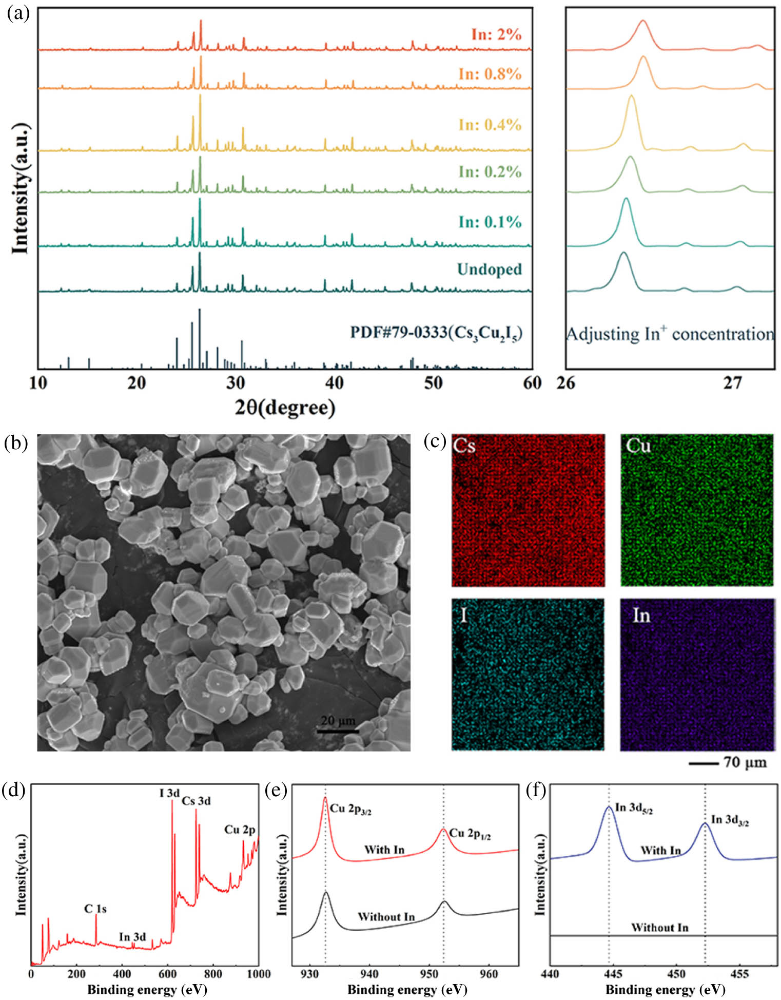
consists of zero-dimensional electronic structures. According to previous theoretical calculations, Cu 3d orbitals dominantly contribute to the valence band maximum (VBM), while the conduction band minimum (CBM) is mainly composed of Cu 4s and I 5p orbitals [45]. Therefore, exciton transition in occurs mainly in the Cu-I structures. The substitution of or ions has become the main strategy for modulating the electronic structure and optical properties of . Considering the ionic radius and spatial configuration of , was proved to be an excellent dopant [43]. In this work, we introduce an additional exciton recombination center in by doping to improve RL efficiency. The phase purity of undoped and In-doped powders was measured by XRD. The prepared powders matched the standard diffractions (PDF#79-0333) exactly, without the existence of impurities [Fig. 1(a)]. With the increase of doping concentration, the XRD peaks shifted continuously toward the higher values of . Compared with the undoped , the strongest diffraction peak of shifted from 26.341 to 26.459 deg implied that doping decreased the interplanar spacing. Figure 1(b) shows the morphology of the powders, an irregular micrometer spherical shape with an average size of 4.16 μm.
Figure 1.Characterization details of the powders. (a) XRD patterns of the powders samples doped with different indium concentrations (top), compared with the orthorhombic at the bottom (PDF#79-0333). (b) SEM image of the powders. (c) Elemental mapping images of the powders. (d) XPS survey spectrum of the powders. (e), (f) High-resolution XPS profiles of Cu ( and ) and In ( and ) of the powders synthesized with and without In, respectively.
The energy dispersive spectroscopy (EDS) and elemental mapping images of the powders are shown in Fig. 1(c), respectively, confirming that the proportions of Cs, Cu, and I atoms were 32.45%, 17.93%, and 48.15%, respectively, close to the stoichiometric ratio (3:2:5). The dopant was also detected at 1.47%. To further determine the composition and chemical state of the elements, we conducted XPS on the powders, showing peaks of the constituting elements C 1s, In 3d, Cs 3d, Cu 2p, and I 3d [Fig. 1(d)]. The valence state of Cu ions in the powders was analyzed in Fig. 1(e). The two peaks located at 932.5 and 952.3 eV were characteristic peaks of and . Moreover, no characteristic satellite peak of was observed (approximately 943 eV), further ruling out the presence of in the powders. Two additional peaks in the InI-doped powders appearing at 444.7 and 452.3 eV attributed to the In 3d further confirmed that was doped into the powders [Fig. 1(f)]. These results provided further support for the successful synthesis of the powders.
B. Ultraviolet Detection Performance of Films
Figure 2(a) shows the optical properties of films. The PLE spectrum of the films showed an excitation peak at 311 nm, while the PL spectrum exhibited strong blue emission at 438 nm with a full-width at half-maximum (FWHM) of 84 nm and a Stokes shift of 127 nm. There was almost no spectral overlap between the PLE and PL spectra, indicating that the prepared materials exhibited ultralow self-absorption [46], which was an indispensable parameter for high-performance scintillators. The PL spectral peaks measured at different doping concentrations showed the same shape but different intensities, indicating that the observed blue emission was caused by radiation recombination in the same excited state [Fig. 2(b)]. As shown in Fig. 2(c), after immersion in deionized water for 1 h, the PL intensity of the films only suffered a slight decay.
Figure 2.Ultraviolet detection performance of the films. (a) PL and PLE spectra of the films. (b) PL emission spectra of the films doped with different indium concentrations. (c) Comparison of the PL spectra of the films before and after being soaked in deionized water for 1 h. (d) PL decay spectra of the films with and without . (e) PLQY spectra of the films. (f) Configuration coordinate diagram of the photophysical dynamics in .
The corresponding TRPL decay curves of the doped and undoped films were measured in Fig. 2(d). The PL lifetime of the films was 0.9 μs, longer than that of the undoped films (0.75 μs), implying that after indium doping, the capture of excited electrons by surface states was inhibited. The efficient utilization of the excited carriers resulted in a high PLQY as well as a long lifetime. A high PLQY of 90.2% was achieved in the films [Fig. 2(e)]. We propose that extra incorporation of brings a new radiative recombination channel and accelerates the energy transfer, improving the utilization of excitons, as well as the PLQY. The high PLQY of the scintillation films ensures a subsequent high RL light yield [44]. Figure 2(f) shows the self-trapped exciton (STE) emission mechanism of the . Under the excitation of an external light source, electrons transitioned from the valence band to the conduction band, and the excited state underwent transient lattice distortion under strong electron phonon coupling, forming the STE state [47]. Due to the low STE barrier, a quantity of electrons relaxed to the STE state, ultimately combining with holes to produce bright blue emissions.
C. X-Ray Detection Performance of Films
Figure 3.X-ray detection performance of the powders. (a) X-ray absorption coefficients of the film, the film, and commercial BGO scintillator as a function of photon energy. (b) RL spectra of the films, the undoped films, and the BGO films (dose rate, 4.85 mGy/s; voltage, 50 kV). The size () and thickness (1 mm) of the films are the same. (c) Dose-rate-dependent RL spectra of the films. (d) Normalized RL intensity of films and BGO under 24 h continuous radiation irradiation with an X-ray dose rate of 7.5 m Gy/s. (e) Signal-to-noise ratio of X-ray response of the films at different irradiation dose rates. (f) MTF of the films, measured by the slanted-edge method.
D. Construction and Application of High-Performance X-Ray Testing System
To demonstrate the potential application of the films in X-ray scintillation, an X-ray image system was constructed with an X-ray source, an X-ray detector, and a computer placed in sequence [Fig. 4(a)]. As a proof-of-concept experiment, the self-made system based on the scintillator film with 220 μm thickness was used to evaluate the X-ray imaging performance. The standard resolution test sample was placed on the films, and we observed the resolution limit of 10 lp/mm, as shown in Fig. 4(b), coinciding well with the calculated MFT result in Fig. 3(f). Through X-ray imaging systems, we could clearly see the fine structures inside the earphone that could not be directly recognized by eyes [Fig. 4(c)]. The internal circuitry of the microchip was revealed in detail, indicating that the films possessed immense potential for application in industrial flaw detection [Fig. 4(d)]. We also imaged the charger and could see its internal structure very clearly, further indicating the films have great potential in imaging detection [Fig. 4(e)]. To evaluate the imaging effect on non-planar objects, we covered a pen with the films. The spring and fill inside the pen could be clearly displayed, and there was no haloing or ghosting [Fig. 4(f)], indicating that the films also had a good imaging effect on the curved surface. This further proved that the flexible films had excellent mechanical stability and could maintain good imaging quality on non-planar objects. These results demonstrated that the films can realize X-ray imaging in complex environments.
Figure 4.Construction and application of a high-performance X-ray testing system. (a) Schematic diagram of the X-ray imaging system. (b) X-ray imaging of the films on the standard resolution card. (c) Photograph and X-ray image (dose rate, 963 μGy/s; tube voltage, 50 kV; beam current, 200 μA; exposure time, 10 s) of internal structure of the earphone; (d) internal circuitry of the microchip; (e) internal structure of the charger plug; (f) internal spring and filling of the pen.
In summary, we demonstrated a facile solution-synthesis route to synthesize high-performance indium-doped perovskite-related X-ray scintillator powders and a flexible scintillator film of at an arbitrary size for X-ray imaging. The film exhibited bright blue light emission with a large Stokes shift of 127 nm and a high PLQY of 90.2%, and achieved good environmental stability. After continuous X-ray irradiation, soaking in deionized water, and continuous bending and stretching, the luminescence and imaging properties of the films remained stable. Benefiting from ultralow self-absorption and high PLQY, a high relative light output was obtained, more than 5 times higher than that of the BGO. The films achieved an ultralow detection limit of 56.2 nGy/s, approximately 98 times lower than the dose of typical X-ray medical imaging. The films also exhibited outstanding X-ray imaging performance, with a high resolution of 11.3 lp/mm, excellent stability under ambient conditions, and undistorted non-planar imaging. To sum up, the presented low-cost, stable, and high-luminous-efficiency flexible scintillator films have great application prospects in high-performance X-ray imaging.
Acknowledgment
Acknowledgment. The authors appreciate the Analytical and Testing Center and Flexible Electronics Research Center of Huazhong University of Science and Technology for the XRD and XPS measurements. The authors also acknowledge the Measurement Laboratory of Collaborative Innovation Center for Digital Intelligent Manufacturing Technology and Application for support in SEM testing.
 AI Video Guide
  AI Picture Guide
 AI One Sentence