• Advanced Photonics
  • Vol. 5, Issue 1, 016004 (2023)
George Giamougiannis1、*, Apostolos Tsakyridis1, Miltiadis Moralis-Pegios1, George Mourgias-Alexandris1, Angelina R. Totovic1, George Dabos1, Manos Kirtas1, Nikolaos Passalis1, Anastasios Tefas1, Dimitrios Kalavrouziotis2, Dimitris Syrivelis2, Paraskevas Bakopoulos2, Elad Mentovich3, David Lazovsky4, and Nikos Pleros1
Author Affiliations
  • 1Aristotle University of Thessaloniki, Department of Informatics, Thessaloniki, Greece
  • 2NVIDIA, Athens, Greece
  • 3NVIDIA, Yokneam, Israel
  • 4Celestial AI, Santa Clara, California, United States
  • show less
    DOI: 10.1117/1.AP.5.1.016004 Cite this Article Set citation alerts
    George Giamougiannis, Apostolos Tsakyridis, Miltiadis Moralis-Pegios, George Mourgias-Alexandris, Angelina R. Totovic, George Dabos, Manos Kirtas, Nikolaos Passalis, Anastasios Tefas, Dimitrios Kalavrouziotis, Dimitris Syrivelis, Paraskevas Bakopoulos, Elad Mentovich, David Lazovsky, Nikos Pleros. Neuromorphic silicon photonics with 50 GHz tiled matrix multiplication for deep-learning applications[J]. Advanced Photonics, 2023, 5(1): 016004 Copy Citation Text show less
    (a)–(c) The process of tiled matrix multiplication. (d) Electro-optic blocks cointegration for the development of a neuromorphic photonic processor with tiled matrix multiplication capabilities. (e) 2:1 hardware implementing a 5:1 neuron in three phases. (f) The tiled MVM process for a 3×5 weight matrix with 5×1 input vectors via 2:1 hardware. (g) The TDM scheme followed during the tiled MVM process of (f).
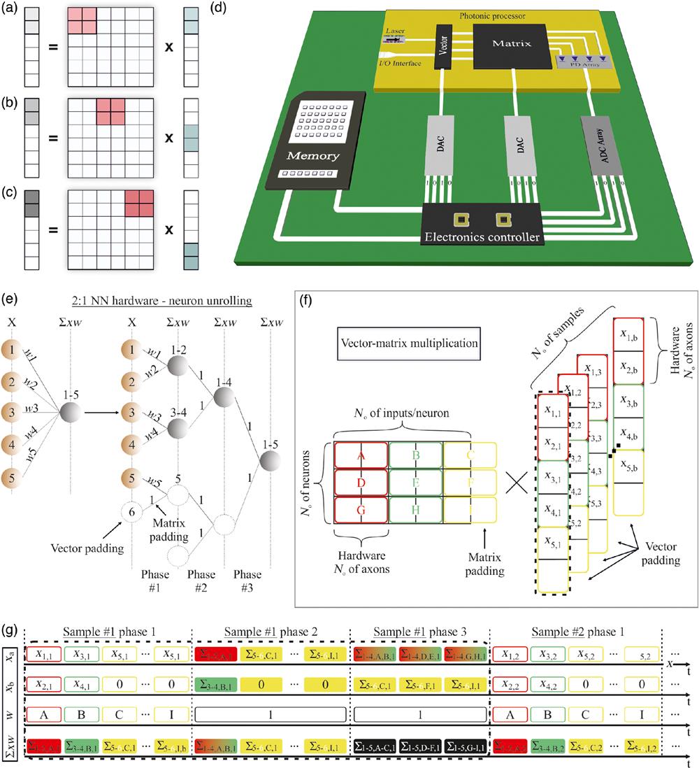
    Fig. 1. (a)–(c) The process of tiled matrix multiplication. (d) Electro-optic blocks cointegration for the development of a neuromorphic photonic processor with tiled matrix multiplication capabilities. (e) 2:1 hardware implementing a 5:1 neuron in three phases. (f) The tiled MVM process for a 3×5 weight matrix with 5×1 input vectors via 2:1 hardware. (g) The TDM scheme followed during the tiled MVM process of (f).
    (a) Microscope top-view photo of the integrated coherent optical linear neuron. The elementary computational cell is encapsulated within a red rectangle. Inset, 2-input neuron realized in the SiPho chip. (b) Experimental setup and visualization of the SiPho chip. (c) Normalized |S21| of the SiGe EAMs deployed in the SiPho processor. (d) Optical loss with respect to the electrical power injected to the PSa.
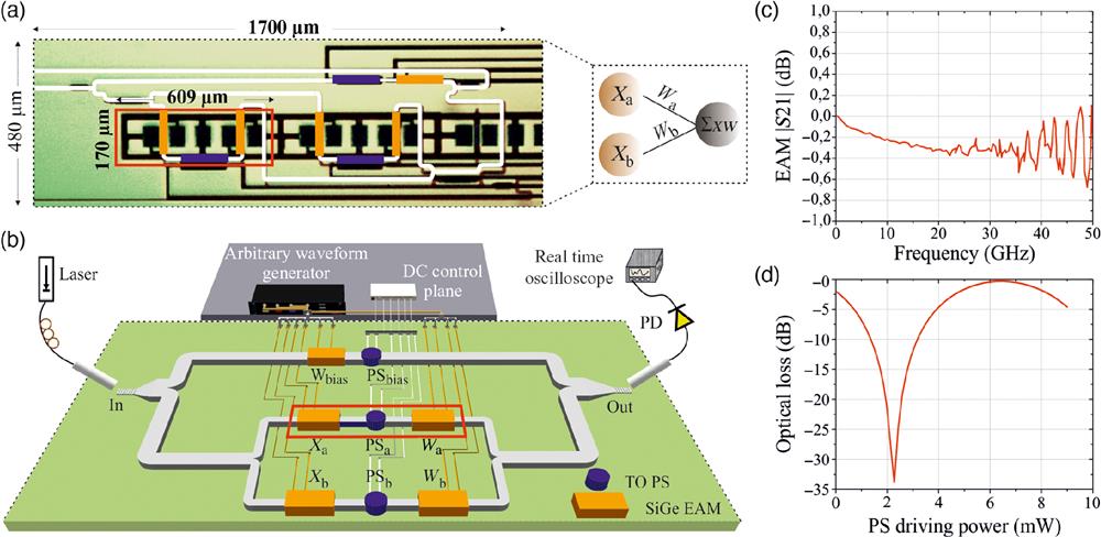
    Fig. 2. (a) Microscope top-view photo of the integrated coherent optical linear neuron. The elementary computational cell is encapsulated within a red rectangle. Inset, 2-input neuron realized in the SiPho chip. (b) Experimental setup and visualization of the SiPho chip. (c) Normalized |S21| of the SiGe EAMs deployed in the SiPho processor. (d) Optical loss with respect to the electrical power injected to the PSa.
    (a) 6:8:2 NN topology for the classification of benign and malicious traffic. (b)–(g) Sample traces obtained at the output of each inference phase, where black dashed lines represent the software-obtained traces and the orange and blue lines correspond to the experimentally obtained traces at 16 and 50 Gbaud, respectively. (h) MSE representation of the 16 and 50 Gbaud experimentally obtained signals per inference phase.
    Fig. 3. (a) 6:8:2 NN topology for the classification of benign and malicious traffic. (b)–(g) Sample traces obtained at the output of each inference phase, where black dashed lines represent the software-obtained traces and the orange and blue lines correspond to the experimentally obtained traces at 16 and 50 Gbaud, respectively. (h) MSE representation of the 16 and 50 Gbaud experimentally obtained signals per inference phase.
    (a) and (b) Experimentally derived confusion matrices of the RA binary classifier at 16 and 50 Gbaud. (c) Equivalent confusion matrix calculated via the software. (d) Experimentally obtained Cohen’s κ-score and SNR of the output layer at 16 and 50 Gbaud.
    Fig. 4. (a) and (b) Experimentally derived confusion matrices of the RA binary classifier at 16 and 50 Gbaud. (c) Equivalent confusion matrix calculated via the software. (d) Experimentally obtained Cohen’s κ-score and SNR of the output layer at 16 and 50 Gbaud.
    (a) N-input COLN. (b) The photonic N×M Xbar layout realizing the weight matrix (blue rectangle) and utilized as an MVM engine onto an N-element input vector (red rectangle). Green rectangle shows the 2:1 MVM architectural part fabricated as a silicon chip with SiGe EAMs for both the input and the weighting stage.
    Fig. 5. (a) N-input COLN. (b) The photonic N×M Xbar layout realizing the weight matrix (blue rectangle) and utilized as an MVM engine onto an N-element input vector (red rectangle). Green rectangle shows the 2:1 MVM architectural part fabricated as a silicon chip with SiGe EAMs for both the input and the weighting stage.
    Square Xbar radix scaling with respect to its IL.
    Fig. 6. Square Xbar radix scaling with respect to its IL.
    George Giamougiannis, Apostolos Tsakyridis, Miltiadis Moralis-Pegios, George Mourgias-Alexandris, Angelina R. Totovic, George Dabos, Manos Kirtas, Nikolaos Passalis, Anastasios Tefas, Dimitrios Kalavrouziotis, Dimitris Syrivelis, Paraskevas Bakopoulos, Elad Mentovich, David Lazovsky, Nikos Pleros. Neuromorphic silicon photonics with 50 GHz tiled matrix multiplication for deep-learning applications[J]. Advanced Photonics, 2023, 5(1): 016004
    Download Citation