Abstract
The explosive volume growth of deep-learning (DL) applications has triggered an era in computing, with neuromorphic photonic platforms promising to merge ultra-high speed and energy efficiency credentials with the brain-inspired computing primitives. The transfer of deep neural networks (DNNs) onto silicon photonic (SiPho) architectures requires, however, an analog computing engine that can perform tiled matrix multiplication (TMM) at line rate to support DL applications with a large number of trainable parameters, similar to the approach followed by state-of-the-art electronic graphics processing units. Herein, we demonstrate an analog SiPho computing engine that relies on a coherent architecture and can perform optical TMM at the record-high speed of 50 GHz. Its potential to support DL applications, where the number of trainable parameters exceeds the available hardware dimensions, is highlighted through a photonic DNN that can reliably detect distributed denial-of-service attacks within a data center with a Cohen’s kappa score-based accuracy of 0.636.1 Introduction
During the last decade, deep neural networks (DNNs) have become increasingly important for the resolution of numerous practical problems.1 With the amount of computing power required to train such DNNs doubling every 3.5 months,2 academic and industrial researchers started gravitating toward new technologies and hardware accelerators to keep pace with this growth. Highly parallelized computing solutions, including graphic processing units (GPUs),3 field programmable gate arrays,4 tensor processing units (TPUs),5 and application-specific integrated circuits,6–8 have been developed to accelerate the matrix-vector multiplication (MVM) operations, which form the most time- and power-consuming computational task in DNNs.9
Yet, as transistor scaling is stagnating,10 a high number of alternative emerging technologies have been investigated toward boosting energy efficiency and performance scaling, e.g., optoelectronic memristors,11–15 nanophotonics,16,17 and spintronics,18,19 with brain-inspired photonic accelerators forming one of the key candidate platforms for future AI computing engines due to their inherent credentials to support time-of-flight latencies and terahertz bandwidths.20,21 Remarkable progress has been witnessed during the last five years in the field of neuromorphic photonics across all necessary constituent technology blocks, including MVM photonic architectures,17,22–28 individual photonic computational elements,29–32 nonlinear activations,33–36 and photonic hardware-aware training models.37,38 All these demonstrations have highlighted the potential for energy-efficient and high-speed DNNs by utilizing low-speed weight encoding technologies and a rather small amount of neurons, validating their credentials to support inference within small scale neural network (NN) topologies that can fit in a practical silicon photonic (SiPho) chip.
However, typical NN layouts used for benchmarking purposes, such as ResNet152 and AlexNet,39 require a total number of 25 and 62 million trainable parameters, respectively, that can hardly fit as hardware-coded information even into the available number of computational elements supported by current top-class GPU and TPU platforms. This has turned tiled matrix multiplication (TMM) into the mainstream processing paradigm in today’s AI engines,40,41 where both the input and the weighting values have to be updated at line rate through time division multiplexing (TDM) approaches until all matrix tiles are processed. To this end, the upgrade of neuromorphic photonics into a versatile AI processing platform has to proceed along the paradigm of today’s TPU and GPU computational engines, where a limited amount of hardware resources can execute DNNs with significantly higher dimensions. This would necessitate, however, the use of photonic architectures and technologies that can support dynamic reconfiguration of both the NN input and weight parameters, with the existing demonstrations being incapable of meeting these requirements, as they mostly rely on low-speed weight encoding technology, such as thermooptic (TO) devices17,26 and phase change materials.22
Sign up for Advanced Photonics TOC. Get the latest issue of Advanced Photonics delivered right to you!Sign up now
In this paper, we present a compact SiPho computing engine that supports both input and weight update rates at a record-high 50 GHz clock frequency, reporting for the first time, to the best of our knowledge, on high-speed TMM directly in the optical domain that allows for DNN implementations over limited-scale photonic hardware. The photonic accelerator comprises a two-input coherent linear neuron (COLN) layout with high-speed SiGe electro-absorption modulators (EAMs) used both for input and weight imprinting. We experimentally demonstrate its credentials to implement TMM and support DNNs with higher dimensions through its deployment in data center (DC) traffic inspection for network security applications, employing the photonic engine for the identification of distributed denial-of-service (DDoS) attack patterns via the classification of reconnaissance attacks (RAs). The DNN comprises 10 neurons and 64 trainable parameters and was successfully executed via the COLN, revealing high experimental accuracy values with a Cohen’s kappa score (-score)42 of 0.638 at 50 GHz. Finally, the scaling perspectives of the EAM-based two-input COLN into a higher dimension coherent photonic crossbar (Xbar) are presented, providing the practical framework for the deployment of optical TMM operations in a layer–scale layout and for higher-dimension tiles.
2 Neuromorphic Processor for Tiled Matrix Multiplication
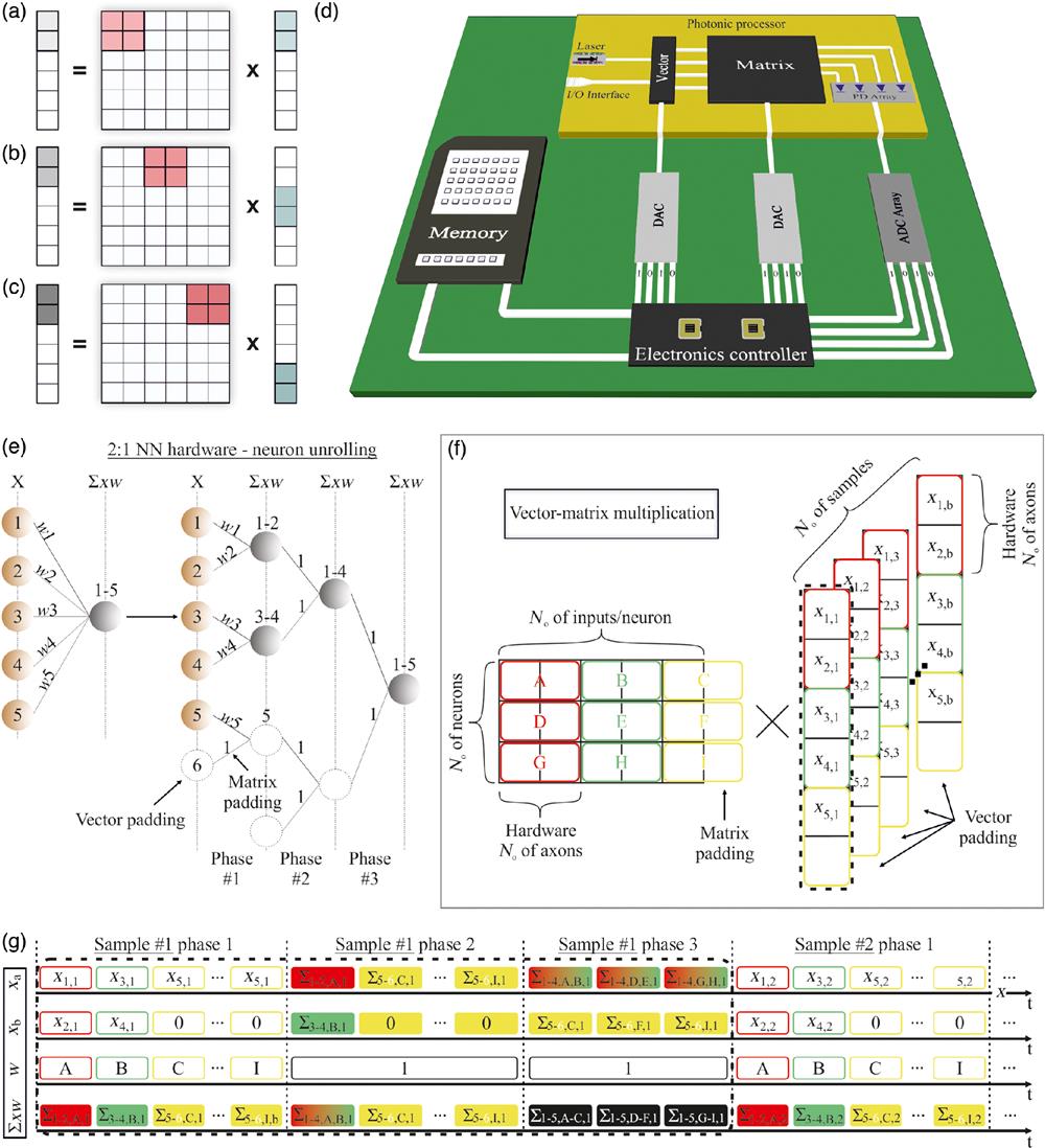
The TMM concept is illustrated in Figs. 1(a)–1(c), showing an example where three different steps are required for calculating the products between two rows of a matrix and a six-element input vector, when matrix tiles are used. The matrix tile starts from the top-left position of the matrix and gets multiplied with the first two input vector values, with the respective products being stored at the first two entries of the six-element output vector, as shown in Fig. 1(a). Then, the matrix tile shifts to the right and the two-element input vector tile shifts down [Fig. 1(b)] to incorporate the next entries of the first two matrix rows and the input vector, respectively, producing in this way two new partial weighted input sums through the multiplication of the tile with the corresponding values of the input vector. This process continues with the tile shifting to the right until the whole horizontal dimension of the matrix has been scanned, as illustrated in Fig. 1(c).

Figure 1.(a)–(c) The process of tiled matrix multiplication. (d) Electro-optic blocks cointegration for the development of a neuromorphic photonic processor with tiled matrix multiplication capabilities. (e) 2:1 hardware implementing a 5:1 neuron in three phases. (f) The tiled MVM process for a weight matrix with input vectors via 2:1 hardware. (g) The TDM scheme followed during the tiled MVM process of (f).
The realization of TMM in the optical domain can be accomplished through a photonic MVM engine where inputs and weights can be updated at line rate, supported by an electronic circuitry for storing the matrix values, loading the necessary tiles to the photonic MVM and storing the partial output sums. This visionary architecture is pictorially represented by Fig. 1(d), showcasing all key building blocks of a neuromorphic photonic processor. The MVM linear operations are executed via the photonic MVM processor in the analog domain, utilizing an integrated or external laser source for “lighting up” the processor. The input and weight values are stored at an electronic memory unit and are loaded onto the photonic MVM processor using digital-to-analog converters. The photonic MVM output is connected to an array of photodiodes that transforms the computed signals back to the electronic domain, exploiting an analog-to-digital converter array for the digitization of the data so that they can be stored at the electronic memory. Additionally, an electronic control circuit is needed for data flow synchronization, orchestration, and communication between the memory block and the photonic MVM unit.
Yet, with the NN depth and size increasing with problem complexity, the total number of the NN-trainable parameters will reach values well beyond the matrix dimensions supported by the photonic MVM engine, implying that the photonic MVM hardware has to be shared among a larger number of parameters through inter/intralayer or intraneuron TDM techniques (see Supplementary Material). The implementation of the above requires either the continuous update of the emerging partial sums for the calculation of the multiplication of a whole input vector with a weight matrix tile, as shown in Figs. 1(a)–1(c), or by storing all partial sums at different registers and then forcing them again for further addition via the photonic MVM engine.
A pictorial example of the intraneuron TDM approach for TMM can be visualized in Fig. 1(e), illustrating how an elementary 2:1 neuron can carry out the linear summations of a five-axon neuron. This corresponds to the dot product between a row vector that contains the weights of the neuron and a column vector that includes the input values, executed through the use of and row and column vector tiles, respectively. The five-input neuron is unrolled into four 2:1 virtual neurons whose linear summation operations can be performed within three phases. More specifically, during the first phase, the 2:1 hardware is utilized in three time slots, calculating the linear summations , , and , with and being zero and one padded input and weight values, respectively. Afterwards, these three partial weighted input sums need to be summed in order to provide the required weighted summation of the five inputs of the neuron. Considering that the addition of the partial sums is carried out again in the optical domain, the summation operation can be performed on-chip by applying weight values equal to 1. Because the hardware can imprint two input values at a time slot, the remaining summations would be performed in two more phases, as depicted in Fig. 1(e). It can be derived that a photonic neuron of number of axons is capable of calculating the linear operations of a layer that comprises neurons of number of inputs each, in phases.
The execution of the MVM product required for an entire neural layer via the same 2:1 NN hardware requires both intraneuron and intralayer TDM, with intraneuron and intralayer TDM corresponding to the use of multiple tiles across a single matrix row and a matrix column, respectively. Assuming, for example, a fully connected layer with number of neurons and number of inputs per neuron, Fig. 1(f) illustrates the MVM between a weight matrix with dimensions and an input vector with dimensions , with being equal to the inference batch size . The 2:1 NN hardware encodes two elements of the weight matrix and two elements of the input vectors at a time slot, highlighted in the colored red, green, and yellow rectangles. This is depicted in more detail in Fig. 1(g), where the NN hardware hosts the weight values of the rectangle A in its weighting modules and , along with the input values and , in the respective input modules and during the first time slot. Both input and weight values will be updated during the second time slot, with the weight values of the matrix tile B being loaded onto the weighting modules and and the input values and onto the respective input and stages. This process continues until all partial weighted input sums of the entire matrix and the first-sample input vector are calculated, i.e., until the last matrix row that comprises matrix tiles , , and gets also multiplied with the input vector from the first sample, completing in this way phase #1 of the process. Subsequently, the partial sums will be sequentially employed at the input modules and for their addition until they form the complete weighted input sum that corresponds to the product between a matrix row and the input vector of the first sample. This process is completed within the subsequent phases #2 and #3 of Fig. 1(g), utilizing weighting values equal to one. After completing phase #3 of the first sample, the multiplication of the weight matrix with the input vector in the second sample is initiated, following again the same TMM scheme and repeating all three phases. The MVM operation will be completed once the entire inference batch size has been processed.
3 Silicon Photonic Coherent Linear Neuron Architecture
Figure 2(a) depicts the SiPho processor that was fabricated for direct on-chip and high-speed mapping of both the input and the weight elements of an NN, following the COLN architecture43 that can implement a dot-product operation. The SiPho chip comprises a coherent neuromorphic architecture that implements a two-input COLN capable of executing multiple-accumulate (MAC) operations, i.e., the weighted summation of its input data. It exploits the interference capabilities of Mach–Zehnder interferometers (MZIs), complemented by a bias branch that safeguards the retention of the sign of the weighted summation (see Supplementary Material). A visualization of the SiPho COLN and the experimental setup established for its evaluation are depicted in Fig. 2(b). Specifically, the SiPho processor comprises five compact and high-bandwidth SiGe EAMs (orange boxes), with two EAMs used in cascade at each MZI branch for on-chip input data and weight imprinting, respectively, and one EAM employed in the bias branch. The selection of the SiGe EAMs allows for a high compute rate, while retaining the energy consumption and the footprint at low values.44,45 The normalized electrooptic response of an EAM biased at is presented in Fig. 2(c), revealing a 1-dB bandwidth higher than 50 GHz. Finally, 3 TO phase shifters (PSs) [blue cylinders in Fig. 2(b)], one at the bias branch and one at each MZI arm, are employed for the application of the sign of the weighted inputs. Figure 2(d) illustrates the optical loss of with respect to the applied driving power, showcasing that is required for π phase shift. Similar behavior was observed in and .
Figure 2.(a) Microscope top-view photo of the integrated coherent optical linear neuron. The elementary computational cell is encapsulated within a red rectangle. Inset, 2-input neuron realized in the SiPho chip. (b) Experimental setup and visualization of the SiPho chip. (c) Normalized |S21| of the SiGe EAMs deployed in the SiPho processor. (d) Optical loss with respect to the electrical power injected to the .
4 Experimental Classification of Benign and Malicious Reconnaissance Attacks Using Photonic TMM at 50 GHz
The NN trained for the RAs classification follows the topology shown in Fig. 3(a). The six features of the port scanned traffic comprise the six inputs of the NN, followed by a fully connected hidden layer (Layer #1) of eight neurons and a two-neuron output layer. The Sigmoid and the SoftMax activation functions were applied to the hidden and output layers, respectively. During the experimental validation of the NN operation, both input and the weight values were updated at the rate of 16 and 50 GHz. Tiled MM was utilized for applying the 64 weight values of the 6:8:2 NN onto the 2:1 SiPho processor, adopting an intralayer and intraneuron TDM approach for calculating the MVM product within Layer #1 before repeating the same process for calculating the MVM products in Layer #2. The accuracy performance of the proposed SiPho neuromorphic prototype was evaluated via the classification of real traffic generated for RA identification (see Supplementary Material).
Figure 3.(a) 6:8:2 NN topology for the classification of benign and malicious traffic. (b)–(g) Sample traces obtained at the output of each inference phase, where black dashed lines represent the software-obtained traces and the orange and blue lines correspond to the experimentally obtained traces at 16 and 50 Gbaud, respectively. (h) MSE representation of the 16 and 50 Gbaud experimentally obtained signals per inference phase.
Figures 3(b)–3(g) illustrate the time multiplexed sample traces obtained at the output of each phase during the experimental inference, with the black dashed lines representing the software-obtained traces, and the orange and blue solid lines corresponding to the experimental traces at 16 and 50 Gbaud, respectively. In particular, Figs. 3(b)–3(d) depict the time multiplexed sample traces that were obtained in the three phases of the first layer, respectively, whereas Figs. 3(e)–3(g) illustrate the time-multiplexed sample traces obtained at each phase of the output layer. Figure 3(h) presents the normalized mean squared errors (MSEs) of the experimentally captured signals per inference phase and per layer. The MSEs of the 16 and 50 Gbaud summations at the last phase of Layer #1 equal and , respectively, while the respective MSE values after the summations of the first phase of Layer#2 are reduced to and , respectively. The MSE is always higher at 50 GHz compared with the 16 GHz operational mode and increases as the process moves from the first to the last phase within the same layer, being the result of the noise accumulation that is associated with the reuse of the photonic processor and the higher noise bandwidth. Yet, the interlayer transition reduces the deviation between the experimental and the reference waveform, decreasing the amount of noise upon entering Layer #2 compared with the noise that was accumulated through all Layer #1 phases. This is the result of the Sigmoid activation function employed at Layer #1 output, which takes advantage of its high nonlinearity at its boundaries to compress the edge values of the samples.
The inference classification performance of our SiPho prototype when performing with 500 samples of the generated traffic was quantified by calculating the -score, which comprises a statistical metric for the evaluation of the inference accuracy when imbalanced data sets are classified (see Supplementary Material), with their confusion matrices depicted in Figs. 4(a)–4(c). The software acquired -score was calculated to be equal to 0.70, and the respective values of the experimental classification at 16 and 50 Gbaud were measured equal to 0.688 and 0.636, as depicted in Fig. 4(d). Finally, the signal-to-noise ratio (SNR) values of the linear summations emerging from the photonic NN (PNN) were measured equal to 14.1 and 11.2 dB, respectively.
Figure 4.(a) and (b) Experimentally derived confusion matrices of the RA binary classifier at 16 and 50 Gbaud. (c) Equivalent confusion matrix calculated via the software. (d) Experimentally obtained Cohen’s -score and SNR of the output layer at 16 and 50 Gbaud.
5 Discussion
The successful proof-of-principle experimental validation of the optical TMM at 16 and 50 GHz and the classification of the RA traffic requires a total number of six TDM phases, which is the result of the 2:1 PNN that, inevitably, necessitates the use of 2:1 matrix tiles. The number of TDM phases required and the associated time overhead can be reduced by scaling the PNN chip into a higher-dimension layout that can host a higher amount of on-chip input and weight modulation elements. Figure 5(a) illustrates how the 2:1 COLN can scale to an neuron by following the layout that has been already mathematically validated and simulated in Ref. 43 and experimentally validated in Refs. 26 and 46. This is based on the introduction of an splitter followed by a stack of parallel waveguides, where every waveguide incorporates a high-speed amplitude modulator for the input signal, followed by a high-speed PS for sign update and a high-speed amplitude modulator for weight update. All these parallel waveguides recombine via an combiner, forming in this way a multibranch interferometer. Extending this architecture into a 2D matrix that can support matrix tiles and further reduce the MVM latency can be realized by adopting an coherent linear photonic Xbar architecture that follows the principles reported in Refs. 47 and 48 and uses EAMs as its input and weight modulation circuitry. The Xbar layout is depicted in Fig. 5(b), with the green rectangle illustrating that the 2:1 COLN utilized in our PNN chip [Fig. 2(a)] comprises a subblock within the design. The Xbar architecture can host neurons with axons per neuron simultaneously, allowing for the use of matrix tiles within the TMM process. The credentials of this architecture to support high-dimension matrix tiles within practical total loss values can be verified through a quantitative theoretical insertion loss (IL) analysis using experimentally measured specifications, assuming a symmetric Xbar that employs SiGe EAMs both for the input and the weight values (see Supplementary Material). As shown in Fig. 6, the total IL of the Xbar architecture increases with increasing matrix dimensions but retains a reasonable value of less than 30 dB, even for a layout, which supports a total amount of 1024 MAC operations. This can scale to higher total MAC capabilities by combining wavelength division multiplexing (WDM) with the coherent Xbar scheme, following the design reported in Refs. 47 and 49, and can support tensor tiles, with representing the number of wavelengths employed. The extension of the 2:1 COLN into an coherent Xbar design retains all its additional benefits with respect to flexibility, robustness, and energy and footprint efficiency50,51 (see also Supplementary Material), as it allows for one-to-one and high-fidelity single-step mapping of the NN parameters onto the PNN hardware48 and the deployment of high-speed nodes’ technology.
Figure 5.(a) -input COLN. (b) The photonic Xbar layout realizing the weight matrix (blue rectangle) and utilized as an MVM engine onto an -element input vector (red rectangle). Green rectangle shows the 2:1 MVM architectural part fabricated as a silicon chip with SiGe EAMs for both the input and the weighting stage.
Figure 6.Square Xbar radix scaling with respect to its IL.
6 Conclusion
Recent advances in SiPhos have enabled the exploitation of light for computing by accelerating the execution of deep-learning algorithms. In this work, we demonstrate an SiPho processor that is capable of performing linear algebra operations of any-dimensioned NN layer towards classifying, at record-high speeds, DDOS attacks within DC server packets. Specifically, by employing the TMM method, we were able to accelerate the MAC operations that take place into the AI processor up to the rate of 50 GHz, detecting successfully benign and malicious attacks with a -score of 0.636. Finally, towards minimizing the computing steps and maximizing the classification speeds, we provide a dimension scaling analysis of the demonstrated prototype into a space division multiplexed Xbar architecture capable of supporting layer-scale linear algebra operations.
George Giamougiannis received his Diploma degree in “Electrical and Computer Engineering” from the Aristotle University of Thessaloniki, Greece, in 2017. At the beginning of 2020 he received his MSc in “Communication Networks and Systems Security” from the same department. Since September 2019, he is a member of the WinPhos research group pursuing his PhD with Prof. Nikos Pleros as his supervisor. His research interests focus on linear optics and neuromorphic photonics and he has (co-)authored 13 journal papers, 15 papers in international conferences, and 3 US patents.
Biographies of the other authors are not available.
References
[1] Y. LeCun, Y. Bengio, G. Hinton. Deep learning. Nature, 521, 436-444(2015).
[2] P. R. Prucnal et al. Multiwavelength neuromorphic photonics(2019).
[3] Z. Chen et al. A fast deep learning system using GPU. IEEE Int. Symp. Circuits and Syst. (ISCAS), 1552-1555(2014).
[4] C. Zhang et al. Optimizing FPGA-based accelerator design for deep convolutional neural networks, 161-170(2015).
[5] Cloud Tensor Processing Units (TPUs)(2023).
[6] L. Cavigelli, L. Benini. Origami: a 803-GOp/s/W convolutional network accelerator. IEEE Trans. Circuits Syst. Video Technol., 27, 2461-2475(2017).
[7] Graphcore(2023).
[8] Groq(2023).
[9] Y. Chen et al. A survey of accelerator architectures for deep neural networks. Engineering, 6, 264-274(2020).
[10] T. N. Theis, H.-S. P. Wong. The end of Moore’s law: a new beginning for information technology. Comput. Sci. Eng., 19, 41-50(2017).
[11] L. X. Hu et al. All-optically controlled memristor for optoelectronic neuromorphic computing. Adv. Funct. Mater., 31, 2005582(2021).
[12] J. Yanh et al. Optically driven intelligent computing with ZnO memristor. Fundam. Res.(2022).
[13] F. Brückerhoff-Plückelmann et al. A large scale photonic matrix processor enabled by charge accumulation. Nanophotonics(2022).
[14] X. Li et al. On-chip phase change optical matrix multiplication core. IEEE Int. Electron Devices Meeting (IEDM), 7.5.1-7.5.4(2020).
[15] K. Portner et al. Analog nanoscale electro-optical synapses for neuromorphic computing applications. ACS Nano, 15, 14776-14785(2021).
[16] V. J. Sorger et al. Ultra-compact silicon nanophotonic modulator with broadband response. Nanophotonics, 1, 17-22(2012).
[17] Y. Shen et al. Deep learning with coherent nanophotonic circuits. Nat. Photonics, 11, 441-446(2017).
[18] J. Grollier et al. Neuromorphic spintronics. Nat. Electron., 3, 360-370(2020).
[19] Z. Guo et al. Spintronics for energy-efficient computing: an overview and outlook. Proc. IEEE, 109, 1398-1417(2021).
[20] M. A. Nahmias et al. Photonic multiply-accumulate operations for neural networks. IEEE J. Sel. Top. Quantum Electron., 26, 7701518(2020).
[21] A. Totovic et al. Femtojoule per MAC neuromorphic photonics: an energy and technology roadmap. IEEE J. Sel. Top. Quantum Electron., 26, 8800115(2020).
[22] J. Feldmann et al. Parallel convolutional processing using an integrated photonic tensor core. Nature, 589, 52-58(2021).
[23] G. Giamougiannis et al. Silicon-integrated coherent neurons with 32GMAC/sec/axon compute line-rates using EAM-based input and weighting cells(2021).
[24] S. Ohno et al. Si microring resonator crossbar array for on-chip inference and training of optical neural network(2021).
[25] C. Huang et al. Demonstration of scalable microring weight bank control for large-scale photonic integrated circuits. APL Photonics, 5, 040803(2020).
[26] G. Mourgias-Alexandris et al. A silicon photonic coherent neuron with 10GMAC/sec processing line-rate, Tu5H.1(2021).
[27] B. Shi, N. Calabretta, R. Stabile. Deep neural network through an InP SOA-based photonic integrated cross-connect. IEEE J. Sel. Top. Quantum Electron., 26, 7701111(2020).
[28] H. Zhang et al. An optical neural chip for implementing complex-valued neural network. Nat. Commun., 12, 457(2021).
[29] W. Zhang et al. Microring weight banks control beyond 8.5-bits accuracy(2021).
[30] J. K. George. Neuromorphic photonics with electro-absorption modulators. Opt. Express, 27, 5181-5191(2019).
[31] C. Wu et al. Programmable phase-change metasurfaces on waveguides for multimode photonic convolutional neural network. Nat. Commun., 12, 96(2021).
[32] G. Dabos et al. Neuromorphic photonic technologies and architectures: scaling opportunities and performance frontiers [Invited]. Opt. Mater. Express, 12, 2343-2367(2022).
[33] G. Mourgias-Alexandris et al. An all-optical neuron with sigmoid activation function. Opt. Express, 27, 9620-9630(2019).
[34] C. Huang et al. Programmable silicon photonic optical thresholder. IEEE Photonics Technol. Lett., 31, 1834-1837(2019).
[35] R. Amin et al. ITO-based electro-absorption modulator for photonic neural activation function. APL Mater., 7, 081112(2019).
[36] I. A. D. Williamson et al. Reprogrammable electro-optic nonlinear activation functions for optical neural networks. IEEE J. Sel. Top. Quantum Electron., 26, 7700412(2019).
[37] M. Moralis-Pegios et al. Neuromorphic silicon photonics and hardware-aware deep learning for high-speed inference. J. Lightwave Technol., 40, 3243-3254(2022).
[38] G. Mourgias-Alexandris et al. Channel response-aware photonic neural network accelerators for high-speed inference through bandwidth-limited optics. Opt. Express, 30, 10664-10671(2022).
[39] I. Kandel, M. Castelli. Transfer learning with convolutional neural networks for diabetic retinopathy image classification: a review. Appl. Sci., 10, 2021(2020).
[40] G. E. Moon et al. Evaluating spatial accelerator architectures with tiled matrix-matrix multiplication. IEEE Trans. Parallel Distrib. Syst., 33, 1002-1014(2022).
[41] NVIDIA app. Note(2023).
[42] M. L. McHugh. Interrater reliability: the kappa statistic. Biochem. Med., 22, 276-282(2012).
[43] G. Mourgias-Alexandris et al. Neuromorphic photonics with coherent linear neurons using dual-IQ modulation cells. J. Lightwave Technol., 38, 811-819(2020).
[44] M. Pantouvaki et al. Active components for 50 Gb/s NRZ-OOK optical interconnects in a silicon photonics platform. J. Lightwave Technol., 35, 631-638(2017).
[45] G. Sinatkas et al. Electro-optic modulation in integrated photonics. J. Appl. Phys., 130, 010901(2021).
[46] H. Zhou et al. Photonic matrix multiplication lights up photonic accelerator and beyond. Light Sci. Appl., 11, 30(2022).
[47] A. Totovic et al. WDM equipped universal linear optics for programmable neuromorphic photonic processors. Neuromorph. Comput. Eng., 2, 024010(2022).
[48] G. Giamougiannis et al. A coherent photonic crossbar for scalable universal linear optics. J. Lightwave Technol.(2022).
[49] A. Totovic et al. Programmable photonic neural networks combining WDM with coherent linear optics. Sci Rep., 12, 5605(2022).
[50] A. Tsakyridis et al. Universal linear optics for ultra-fast neuromorphic silicon photonics towards Fj/MAC and TMAC/sec/mm2 engines. IEEE J. Sel. Top. Quantum Electron., 28, 8300815(2022).
[51] G. Giamougiannis et al. Universal linear optics revisited: new perspectives for neuromorphic computing with silicon photonics. IEEE J. Sel. Top. Quantum Electron., 28, 6200116(2022).
[52] J. Zhang et al. Deep learning based attack detection for cyber-physical system cybersecurity: a survey. IEEE/CAA J. Autom. Sin., 9, 377-391(2022).
[53] M. Ge et al. Deep learning-based intrusion detection for IoT networks. IEEE 24th Pac. Rim Int. Symp. Depend. Comput. (PRDC), 256-25609(2019).
[54] Z. Sheng et al. A compact and low-loss MMI coupler fabricated with CMOS technology. IEEE Photonics J., 4, 2272-2277(2012).
[55] B. Sharma et al. Design and simulation of ultra-low loss triple tapered asymmetric directional coupler at 1330 nm. Microelectron. J., 107, 104957(2021).
[56] Y. Ma et al. Ultralow loss single layer submicron silicon waveguide crossing for SOI optical interconnect. Opt. Express, 21, 29374-29382(2013).