• Journal of Semiconductors
  • Vol. 40, Issue 8, 081507 (2019)
Jing Teng1、2, Nan Liu1、2, and Yongqing Li1、2、3
Author Affiliations
  • 1Beijing National Laboratory for Condensed Matter Physics, Institute of Physics, Chinese Academy of Sciences, Beijing 100190, China
  • 2School of Physical Sciences, University of Chinese Academy of Sciences, Beijing 100049, China
  • 3Songshan Lake Materials Laboratory, Dongguan 523808, China
  • show less
    DOI: 10.1088/1674-4926/40/8/081507 Cite this Article
    Jing Teng, Nan Liu, Yongqing Li. Mn-doped topological insulators: a review[J]. Journal of Semiconductors, 2019, 40(8): 081507 Copy Citation Text show less
    (Color online) Schematics of (a) a massless (m = 0) and (b) a massive (m ≠ 0) surface state of a 3D TI as for the time-reversal symmetry (TRS) broken by the introduction of effective magnetic interaction into the system.
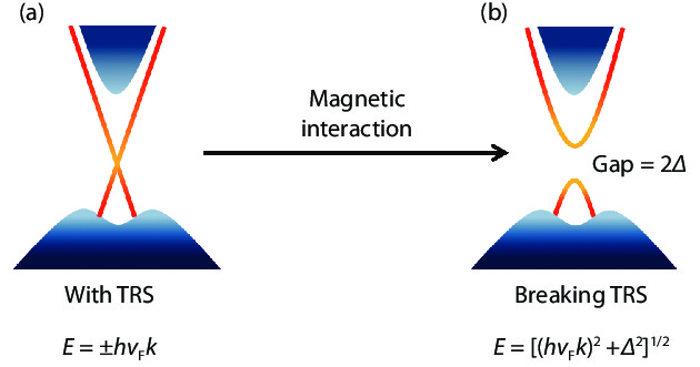
    Fig. 1. (Color online) Schematics of (a) a massless (m = 0) and (b) a massive (m ≠ 0) surface state of a 3D TI as for the time-reversal symmetry (TRS) broken by the introduction of effective magnetic interaction into the system.
    (Color online) STM image of Mn doped Bi2Te3 (x = 0.09). Adapted from Ref. [50]. (a) STM topograph of Bi1.91Mn0.09Te3 (001) surface, +250 meV, 40 pA, 1000 × 1000 Å2. Substitutional Mn atoms appear as triangular suppressions of the LDOS. (b) and (c) Zoom-in topographies over Mn dopants of unoccupied (+500 mV, 30 pA) and filled states (−500 mV, 30 pA), 30 × 30 Å2. Reprinted with permission from Ref. [50].
    Fig. 2. (Color online) STM image of Mn doped Bi2Te3 (x = 0.09). Adapted from Ref. [50]. (a) STM topograph of Bi1.91Mn0.09Te3 (001) surface, +250 meV, 40 pA, 1000 × 1000 Å2. Substitutional Mn atoms appear as triangular suppressions of the LDOS. (b) and (c) Zoom-in topographies over Mn dopants of unoccupied (+500 mV, 30 pA) and filled states (−500 mV, 30 pA), 30 × 30 Å2. Reprinted with permission from Ref. [50].
    (Color online) Adapted from Ref. [42]. (a) X Ray Diffraction of undoped and Mn-doped Bi2Te3 thin films. (b) A high-angle annular dark field (HAADF) scanning transmission electron microscopy (STEM) image of (Bi1–xMnx)2Te3 thin film (5% Mn concentration). Dotted yellow lines indicate QLs and unit layers composed of a Bi bilayer sandwiched between two QLs. (c) Atomic crystal structures of QL–Bi2–QL. (d) Atomic crystal structures of Bi2Te3 QLs with Bi partially substituted by Mn. Reprinted with permission from Ref. [42].
    Fig. 3. (Color online) Adapted from Ref. [42]. (a) X Ray Diffraction of undoped and Mn-doped Bi2Te3 thin films. (b) A high-angle annular dark field (HAADF) scanning transmission electron microscopy (STEM) image of (Bi1–xMnx)2Te3 thin film (5% Mn concentration). Dotted yellow lines indicate QLs and unit layers composed of a Bi bilayer sandwiched between two QLs. (c) Atomic crystal structures of QL–Bi2–QL. (d) Atomic crystal structures of Bi2Te3 QLs with Bi partially substituted by Mn. Reprinted with permission from Ref. [42].
    (Color online) A proposed process for the self-assembly of Bi2Se3 layers interspersed with septuple Bi2MnSe4. Adapted from Ref. [44]. (a) Bi, Se, and Mn atoms arrival at the growth surface. (b) Bi2Se3 forms thermodynamically while Mn atoms remain diffuse until pairing with Se atoms. (c) Self-assembling of Bi2MnSe4 SLs as interspersing between Bi2Se3 QLs. STEM image of 2.5% (d) and 4.2% Mn doped Bi2Se3 (e) showing the layered structure of Mn doped Bi2Se3. Reprinted with permission from Ref. [44].
    Fig. 4. (Color online) A proposed process for the self-assembly of Bi2Se3 layers interspersed with septuple Bi2MnSe4. Adapted from Ref. [44]. (a) Bi, Se, and Mn atoms arrival at the growth surface. (b) Bi2Se3 forms thermodynamically while Mn atoms remain diffuse until pairing with Se atoms. (c) Self-assembling of Bi2MnSe4 SLs as interspersing between Bi2Se3 QLs. STEM image of 2.5% (d) and 4.2% Mn doped Bi2Se3 (e) showing the layered structure of Mn doped Bi2Se3. Reprinted with permission from Ref. [44].
    (Color online) HR-STEM images of Mn doped Bi2Te3 and Bi2Se3[38], showing the layered heterostructure consisting of Bi2MnTe4 (Bi2MnSe4) SLs inserted between Bi2Te3 (Bi2Se3) QLs. Reprinted with permission from Ref. [38].
    Fig. 5. (Color online) HR-STEM images of Mn doped Bi2Te3 and Bi2Se3[38], showing the layered heterostructure consisting of Bi2MnTe4 (Bi2MnSe4) SLs inserted between Bi2Te3 (Bi2Se3) QLs. Reprinted with permission from Ref. [38].
    (Color online) ARPES shows gap opening in the Dirac surface states of Mn doped Bi2Se3[36]. (a) ARPES spectra of of (Bi0.99Mn0.01)2Se3 single crystal along K–Γ–K. Inset is a close-up of the dispersion in the vicinity of EF, indicating a gap between the leading edge of the surface state band and EF. (b) A leading-edge gap of 7 meV by comparison between the Γ point EDC and EF. Reprinted with permission from Ref. [36].
    Fig. 6. (Color online) ARPES shows gap opening in the Dirac surface states of Mn doped Bi2Se3[36]. (a) ARPES spectra of of (Bi0.99Mn0.01)2Se3 single crystal along K–Γ–K. Inset is a close-up of the dispersion in the vicinity of EF, indicating a gap between the leading edge of the surface state band and EF. (b) A leading-edge gap of 7 meV by comparison between the Γ point EDC and EF. Reprinted with permission from Ref. [36].
    (Color online) Spin-resolved ARPES of Mn doped Bi2Se3. Adapted from Ref. [37]. (a) Spin-integrated data and (b) corresponding MDCs on film I (20 eV photons, MDC mode). (c) Spin-integrated dispersion and corresponding EDCs on film II (9 eV photons, EDC mode). Reprinted with permission from Ref. [37].
    Fig. 7. (Color online) Spin-resolved ARPES of Mn doped Bi2Se3. Adapted from Ref. [37]. (a) Spin-integrated data and (b) corresponding MDCs on film I (20 eV photons, MDC mode). (c) Spin-integrated dispersion and corresponding EDCs on film II (9 eV photons, EDC mode). Reprinted with permission from Ref. [37].
    (Color online) ARPES measurements of (Bi1–xMnx)2Se3 with different Mn doping and temperature. Adapted from Ref. [60]. (a–d) Mn doping-dependent ARPES for x values of (a) 0, (b) 0.02, (c) 0.04 and (d) 0.08, 50 eV photon energy, 12 K. The surface band gap increases with increasing Mn content. (e, f) ARPES dispersions of (Bi1–xMnx)2Se3 (x = 8%) at temperature of (e) 12 K and (f) 300 K. The surface band gap does not show a remarkable temperature dependence. Reprinted with permission from Ref. [60].
    Fig. 8. (Color online) ARPES measurements of (Bi1–xMnx)2Se3 with different Mn doping and temperature. Adapted from Ref. [60]. (a–d) Mn doping-dependent ARPES for x values of (a) 0, (b) 0.02, (c) 0.04 and (d) 0.08, 50 eV photon energy, 12 K. The surface band gap increases with increasing Mn content. (e, f) ARPES dispersions of (Bi1–xMnx)2Se3 (x = 8%) at temperature of (e) 12 K and (f) 300 K. The surface band gap does not show a remarkable temperature dependence. Reprinted with permission from Ref. [60].
    (Color online) Magnetic gap of Mn-doped Bi2Te3 derived by ARPES. Adapted from Ref. [38]. (a–d) Measurements for Bi2Te3 with 6% Mn performed above and below the Curie temperature TC ~ 10 K. Linear fits to the regions indicated in (c) yield shifts of 21 and 12 meV between these sections of the 20 and 1 K spectra. (d) Simulation showing that this corresponds to a magnetic gap = 90 ± 10 meV. (e–g) Same analysis for Mn doped Bi2Se3 with 6% Mn and a TC of 6 K, revealing only a nonmagnetic gap of 220 ± 5 meV at 20 K and 205 ± 5 meV at 1 K, determined by least-square fit to the upper Dirac cone and to the lower Dirac cone at k// = 0 Å–1. Reprinted with permission from Ref. [38]
    Fig. 9. (Color online) Magnetic gap of Mn-doped Bi2Te3 derived by ARPES. Adapted from Ref. [38]. (a–d) Measurements for Bi2Te3 with 6% Mn performed above and below the Curie temperature TC ~ 10 K. Linear fits to the regions indicated in (c) yield shifts of 21 and 12 meV between these sections of the 20 and 1 K spectra. (d) Simulation showing that this corresponds to a magnetic gap = 90 ± 10 meV. (e–g) Same analysis for Mn doped Bi2Se3 with 6% Mn and a TC of 6 K, revealing only a nonmagnetic gap of 220 ± 5 meV at 20 K and 205 ± 5 meV at 1 K, determined by least-square fit to the upper Dirac cone and to the lower Dirac cone at k// = 0 Å–1. Reprinted with permission from Ref. [38]
    (Color online) Magnetic-field-dependent magnetization of (Bi1–xMnx)2Te3 crystal (x = 0.045) with in-plane and out-of-plane fields, T = 1.8 K. Inset is the low field hysteresis MH loops of this Bi1.91Mn0.09Te3 crystal. Reprinted with permission from Ref. [50].
    Fig. 10. (Color online) Magnetic-field-dependent magnetization of (Bi1–xMnx)2Te3 crystal (x = 0.045) with in-plane and out-of-plane fields, T = 1.8 K. Inset is the low field hysteresis MH loops of this Bi1.91Mn0.09Te3 crystal. Reprinted with permission from Ref. [50].
    (Color online) SQUID measurements of (Bi1–xMnx)2Se3. Adapted from Ref. [45]. (a) Temperature-dependent magnetization curves (M–T) of the Bi/Mn = 12.5 sample. (b) Field-dependent magnetization plots (M–H) of the Bi/Mn = 12.5 sample with in-plane field at different temperatures. (c) M–H of the Bi/Mn = 12.5 sample with out-of-plane field at different temperatures. (d) M–T of the Bi/Mn = 23.6 sample. (e) M–H of the Bi/Mn = 23.6 sample with in-plane field at different temperatures. (f) M–H of the Bi/Mn = 23.6 sample with out-of-plane field at different temperatures. Reprinted with permission from Ref. [45].
    Fig. 11. (Color online) SQUID measurements of (Bi1–xMnx)2Se3. Adapted from Ref. [45]. (a) Temperature-dependent magnetization curves (MT) of the Bi/Mn = 12.5 sample. (b) Field-dependent magnetization plots (MH) of the Bi/Mn = 12.5 sample with in-plane field at different temperatures. (c) MH of the Bi/Mn = 12.5 sample with out-of-plane field at different temperatures. (d) MT of the Bi/Mn = 23.6 sample. (e) MH of the Bi/Mn = 23.6 sample with in-plane field at different temperatures. (f) MH of the Bi/Mn = 23.6 sample with out-of-plane field at different temperatures. Reprinted with permission from Ref. [45].
    (Color online) Magnetization M(H) and Anomalous Hall effect (AHE) of Mn doped Bi2Te3 and Bi2Se3. Adapted from Ref. [38]. In-plane and out-of-plane M(H) of Bi2Te3 (a) and Bi2Se3 (b) films with Mn concentrations of 3 and 4% measured at 2 K by SQUID with the magnetic field either parallel or perpendicular to the surface, evidencing a perpendicular anisotropy (easy axis) for Bi2Te3 and an in-plane easy axis for Bi2Se3. The Curie temperature as a function of Mn concentration is depicted in the inserts, evidencing that TC is significantly higher in the telluride system. (c, d) AHE measurements of the samples with the contribution of the ordinary Hall effect extracted from the high field data subtracted. Due to the perpendicular magnetic anisotropy, only Mn-doped Bi2Te3 displays a pronounced anomalous Hall effect appearing when the sample is cooled below TC. Reprinted with permission from Ref. [38]
    Fig. 12. (Color online) Magnetization M(H) and Anomalous Hall effect (AHE) of Mn doped Bi2Te3 and Bi2Se3. Adapted from Ref. [38]. In-plane and out-of-plane M(H) of Bi2Te3 (a) and Bi2Se3 (b) films with Mn concentrations of 3 and 4% measured at 2 K by SQUID with the magnetic field either parallel or perpendicular to the surface, evidencing a perpendicular anisotropy (easy axis) for Bi2Te3 and an in-plane easy axis for Bi2Se3. The Curie temperature as a function of Mn concentration is depicted in the inserts, evidencing that TC is significantly higher in the telluride system. (c, d) AHE measurements of the samples with the contribution of the ordinary Hall effect extracted from the high field data subtracted. Due to the perpendicular magnetic anisotropy, only Mn-doped Bi2Te3 displays a pronounced anomalous Hall effect appearing when the sample is cooled below TC. Reprinted with permission from Ref. [38]
    (Color online) AHE and TC of MnxBi2–xTe3–ySey single crystal (x = 0.04 and y = 0.12) at different carrier density tuned by gating. Adapted from Ref. [65]. (a) Hall conductivity σxy of device A at different back-gate voltages VB. AHE increases with depleting carriers. (b) After application of a top-gate voltage VT = –3 V, device B shows an enhanced σxy. The ordinary Hall conductivity changes from n-type to p-type at the most negative VB. (c) Temperature-dependent σxy of device C. (d) TC of devices A–E on the carrier density. Reprinted with permission from Ref. [65].
    Fig. 13. (Color online) AHE and TC of MnxBi2–xTe3–ySey single crystal (x = 0.04 and y = 0.12) at different carrier density tuned by gating. Adapted from Ref. [65]. (a) Hall conductivity σxy of device A at different back-gate voltages VB. AHE increases with depleting carriers. (b) After application of a top-gate voltage VT = –3 V, device B shows an enhanced σxy. The ordinary Hall conductivity changes from n-type to p-type at the most negative VB. (c) Temperature-dependent σxy of device C. (d) TC of devices A–E on the carrier density. Reprinted with permission from Ref. [65].
    (Color online) Magnetoconductivity of MnxBi2–xTe3–ySey (x = 0.04 and y = 0.12) with gating. Adapted from Ref. [65]. (a) σxx(B) at different VB. (b) σxx(B) at VB = –100 V. (c) Schematic of the domain structure in a magnetic topological insulator. A chiral mode appears in the domain walls across the opposite M domains. (d) σxx(B) at different temperatures at VB = –100 V. (e) σxx(B) shows hysteresis at high carrier density. (f) The difference between the virgin and trained σxx. Reprinted with permission from Ref. [65].
    Fig. 14. (Color online) Magnetoconductivity of MnxBi2–xTe3–ySey (x = 0.04 and y = 0.12) with gating. Adapted from Ref. [65]. (a) σxx(B) at different VB. (b) σxx(B) at VB = –100 V. (c) Schematic of the domain structure in a magnetic topological insulator. A chiral mode appears in the domain walls across the opposite M domains. (d) σxx(B) at different temperatures at VB = –100 V. (e) σxx(B) shows hysteresis at high carrier density. (f) The difference between the virgin and trained σxx. Reprinted with permission from Ref. [65].
    (Color online) Hall conductivity σxy and longitudinal conductivity σxx of Mn-Bi2Te3 films. Adapted from Ref. [42]. (a)–(c) Temperature dependence of σxy with Mn doping 2% (S3), 5% (S4), and 10% (S5). (d) Schematic of the Hall device. (e) Photo image of a Hall bar. (f) σxy with different Mn doping, T = 0.5 K. (g) Temperature dependence of σxy at zero magnetic field with different Mn concentrations. (h) Temperature dependence of σxx. (i) σxx (red) and σxy (black) at 0.5 K. Reprinted with permission from Ref. [42].
    Fig. 15. (Color online) Hall conductivity σxy and longitudinal conductivity σxx of Mn-Bi2Te3 films. Adapted from Ref. [42]. (a)–(c) Temperature dependence of σxy with Mn doping 2% (S3), 5% (S4), and 10% (S5). (d) Schematic of the Hall device. (e) Photo image of a Hall bar. (f) σxy with different Mn doping, T = 0.5 K. (g) Temperature dependence of σxy at zero magnetic field with different Mn concentrations. (h) Temperature dependence of σxx. (i) σxx (red) and σxy (black) at 0.5 K. Reprinted with permission from Ref. [42].
    (Color online) Magneto-transport of Mn-Bi2Se3 thin films. Adapted from Ref. [45]. (a) Measurement geometry. (b) –H curves at different field directions in xz plane. (c) Rxx–H plots under field (θ = 5° and ϕ = 0) at different temperatures. (d) Rxx–H in xy plane at different temperatures. Reprinted with permission from Ref. [45].
    Fig. 16. (Color online) Magneto-transport of Mn-Bi2Se3 thin films. Adapted from Ref. [45]. (a) Measurement geometry. (b) H curves at different field directions in xz plane. (c) RxxH plots under field (θ = 5° and ϕ = 0) at different temperatures. (d) RxxH in xy plane at different temperatures. Reprinted with permission from Ref. [45].
    (Color online) Evolution of the Hall effect and the corresponding AH resistances with Mn concentration (a) and gate-voltage tuning (b). Adapted from Ref. [61]. The magnetic field dependences of the Hall resistance Ryx and the nonlinear part of the Hall resistance (RAH(B) = Ryx(B) – RHB) are shown in the top panels and bottom panels of (a) and (b) respectively. The AH resistance RAH is separated into a positive component (orange line) and a negative one (blue line). The right panels show the schematic band diagrams of the Fermi level changing with doping and gate-voltage tuning.
    Fig. 17. (Color online) Evolution of the Hall effect and the corresponding AH resistances with Mn concentration (a) and gate-voltage tuning (b). Adapted from Ref. [61]. The magnetic field dependences of the Hall resistance Ryx and the nonlinear part of the Hall resistance (RAH(B) = Ryx(B) – RHB) are shown in the top panels and bottom panels of (a) and (b) respectively. The AH resistance RAH is separated into a positive component (orange line) and a negative one (blue line). The right panels show the schematic band diagrams of the Fermi level changing with doping and gate-voltage tuning.
    (Color online) Characteristics of the AH conductivity in a lightly doped (Bi1−xMnx)2Se3 sample (x = 0.02). Adapted from Ref. [61]. (a) and (b) σxx dependences of the magnitudes of the positive and negative AH conductivities above the saturation fields, σAH,1 (panel a) and σAH,2 (panel b). (c) The ratio of the AH components, σAH,2/σAH,2, plotted as a function of σxx. Inset shows the schematic band diagrams for high and low Fermi levels.
    Fig. 18. (Color online) Characteristics of the AH conductivity in a lightly doped (Bi1−xMnx)2Se3 sample (x = 0.02). Adapted from Ref. [61]. (a) and (b) σxx dependences of the magnitudes of the positive and negative AH conductivities above the saturation fields, σAH,1 (panel a) and σAH,2 (panel b). (c) The ratio of the AH components, σAH,2AH,2, plotted as a function of σxx. Inset shows the schematic band diagrams for high and low Fermi levels.
    Chemical formulaDoping concentrationMagnetometryTc (K) Easy axisMechanismRef.
    (Bi1−xMnx)2Te30.04–0.10PPMS9–12Surface normal[50]
    (Bi1−xMnx)2Te30.09,0.15SQUID, torque, muSR9–13Surface normal[63]
    (Bi1−xMnx)2Te30.02–0.10SQUID13.8–17Surface normalVan Vleck type[42]
    (Bi1−xMnx)2Te30.04–0.09ESR12Surface normalRKKY[52]
    (Bi1−xMnx)2Te30.03–0.14XMCD7–15Surface normal[38]
    Bi2−xMnxTe3−ySey0.04magnetotransport13Surface normalRKKY[65]
    (Bi1−xMnx)2Te30.07SQUID5.4In-plane[45]
    (Bi1−xMnx)2Se30.01FMR, PNR6In-planeRKKY[51]
    (Bi1−xMnx)2Se30.06–0.14SQUID< 7In-plane[62]
    (Bi1−xMnx)2Se30.025XMCDUp to 45 KSurface normal[37]
    (Bi1−xMnx)2Se30.075XMCD1.5 KIn-plane[59]
    (Bi1−xMnx)2Se30.04–0.14XMCD5–7In-plane[38]
    Table 1. Magnetic characteristics of Mn doped TIs.
    DopantTICarrier typeSign of Reference
    Cr (22%)Bi2Te3n+[71]
    Cr (15%)(BixSb1–x)2Te3p n +[72]
    V (13%)Sb2Te3p+[35]
    Cr (4%–22%)Bi2Se3n[73]
    Mn (5%–20%)Bi2Te3n[42]
    Mn (4%)Bi2(Te,Se)3n[65]
    Mn (1%–9%)Bi2Se3n– (surface), +(bulk)[61]
    Table 2. The AHE sign in magnetically doped Tis.
    Jing Teng, Nan Liu, Yongqing Li. Mn-doped topological insulators: a review[J]. Journal of Semiconductors, 2019, 40(8): 081507
    Download Citation