Xiu-Yan Fu, Zhao-Di Chen, Dong-Dong Han, Yong-Lai Zhang, Hong Xia, Hong-Bo Sun. Laser fabrication of graphene-based supercapacitors[J]. Photonics Research, 2020, 8(4): 577
Search by keywords or author
- Photonics Research
- Vol. 8, Issue 4, 577 (2020)
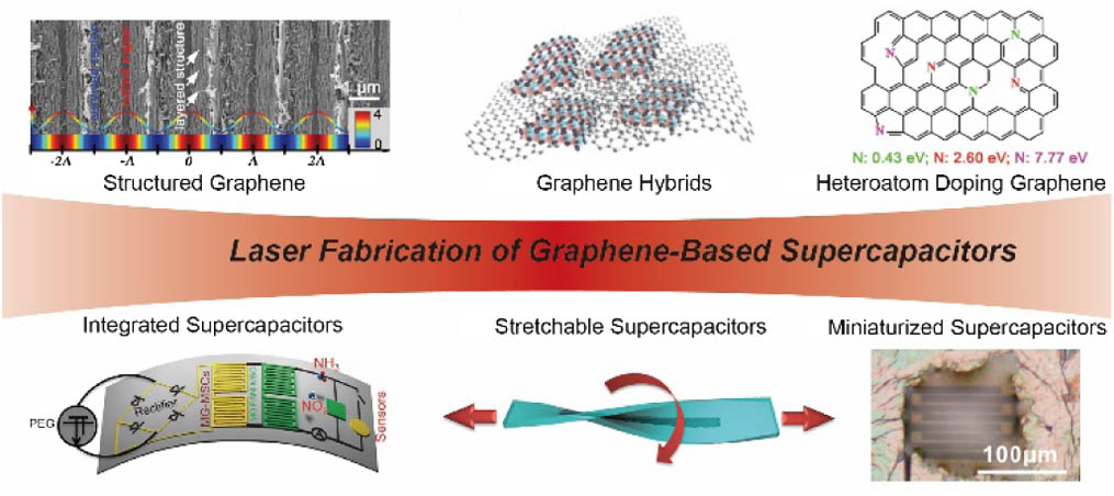
![Progress in laser fabrication of G-SCs. The structured graphene image, adapted from Ref. [56]; the graphene hybrid image, adapted from Ref. [57]; heteroatom doping graphene image, adapted from Ref. [58]; the miniaturized SC image, adapted from Ref. [59]; the stretchable SC image, adapted from Ref. [60]; the integrated SC image, adapted from Ref. [61].](/richHtml/prj/2020/8/4/04000577/img_001.jpg)
Fig. 1. Progress in laser fabrication of G-SCs. The structured graphene image, adapted from Ref. [56]; the graphene hybrid image, adapted from Ref. [57]; heteroatom doping graphene image, adapted from Ref. [58]; the miniaturized SC image, adapted from Ref. [59]; the stretchable SC image, adapted from Ref. [60]; the integrated SC image, adapted from Ref. [61].
![Working mechanism of SCs including (a) EDLCs and (b) pseudo-capacitors; adapted from Ref. [62].](/richHtml/prj/2020/8/4/04000577/img_002.jpg)
Fig. 2. Working mechanism of SCs including (a) EDLCs and (b) pseudo-capacitors; adapted from Ref. [62].
Fig. 3. (a) Schematic illustration of LRGO, adapted from Ref. [67]; (b) schematics and photos of planar and sandwiched LRGO electrodes on GO paper; (c) CV plots of planar and sandwich SCs (scan rate, 40 mV/s); (d) impedance spectra for the in-plane and sandwich devices; (b)–(d) adapted from Ref. [87].
Fig. 4. (a) Scheme for the preparation of graphene-based microsupercapacitors (G-MSCs); (b) CV curves of G-MSCs on PET substrates and (c) corresponding areal and volumetric capacitances at different scan rates; adapted from Ref. [59].
Fig. 5. (a) Diagram of LIG converted from PI; (b) scanning electron microscope (SEM) image of the as-prepared owl-shaped LIG pattern; scale bar, 1 mm; (c) Raman spectra and (d) XRD patterns of LIG and PI; (e) high-resolution transmission electron microscope (HRTEM) image of LIG; scale bar, 5 nm; (f) transmission electron microscope (TEM) image of selected area of LIG, scale bar, 5 Å; adapted from Ref. [101].
Fig. 6. (a) Diagram of LSG-based electrochemical capacitors, adapted from Ref. [106]; (b) schematic illustration of fabricating LRGO films with 1D grating structures by the TBLI technique; (c) SEM image; (d) atomic force microscope (AFM) image of LRGO films with 1D grating-like structures; (b)–(d) adapted from Ref. [56].
Fig. 7. (a) Photo of molybdenum carbide-graphene (MCG) fabricated by DLW on paper substrate; (b) schematic illustration of the MCG fabrication process; (c) CV curves of interdigital SC; (d) CV curves of single, parallel, and series sandwich-structure devices measured at a scan rate of 100 mV/s; adapted from Ref. [57].
Fig. 8. (a) Illustration of the preparation of boron-doped LIG MSCs (B-LIG-MSCs); (b) B 1s spectrum and (c) N 1s spectrum of B-LIG; (d) CV curves of LIG-MSC and B-LIG-MSC; scan rate 0.1 V/s; (e) galvanostatic charge-discharge (GCD) curves of LIG-MSC and B-LIG-MSC; current density 1 mA / cm 2
Fig. 9. (a) Fabrication process for miniaturized SCs by using a femtosecond laser; (b) RGO electrode arrays with a spacing of 2 μm; (c) optical microscope image of microelectrolyte droplets covering the electrode; CV plots of RGO MSC with interelectrode spacing of (d) 2 μm and (e) 550 μm; adapted from Ref. [61].
Fig. 10. (a) Schematic illustration of a highly stretchable SC using LIG electrode onto elastomeric substrate; (b) device structure; CV plots of SCs under (c) stretching and (d) bending tests; scan rate 10 V/s; adapted from Ref. [60].
Fig. 11. (a) Illustration of an integrated device including SCs and sensors; (b) photograph of the integrated device; (c) charging and discharging curve of the MG-MSCs and discharging curves of the MG-PANI MSCs; (d) leakage currents of MSCs; adapted from Ref. [59].

Set citation alerts for the article
Please enter your email address


