
Zengyi Xu, Xianhao Lin, Zhiteng Luo, Qianying Lin, Jianli Zhang, Guangxu Wang, Xiaolan Wang, Fengyi Jiang, Ziwei Li, Jianyang Shi, Junwen Zhang, Chao Shen, Nan Chi, "Flexible 2 × 2 multiple access visible light communication system based on an integrated parallel GaN/InGaN micro-photodetector array module," Photonics Res. 12, 793 (2024)
- Photonics Research
- Vol. 12, Issue 4, 793 (2024)
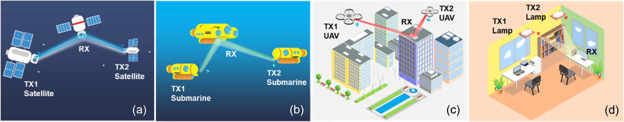
Fig. 1. Illustrations of the potential scenarios of superposed modulation in (a) satellite network VLLC, (b) underwater VLLC, (c) UAV and terrestrial VLLC, and (d) indoor VLLC.
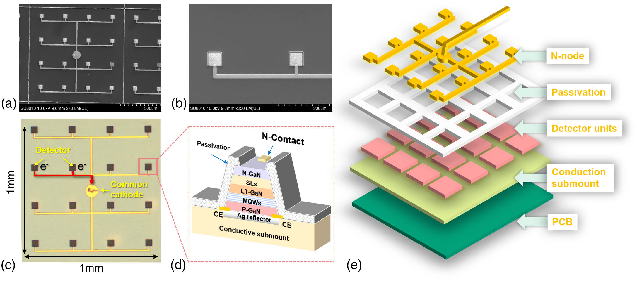
Fig. 2. (a) SEM images of the proposed micro-PD array. (b) The detailed SEM images of two detectors. (c) The optical microscopic image of the PD array chip. All cathodes on this chip are connected into the common cathode located at the center of the chip. (d) The intersection of a single detector unit, showing its layer structure. (e) The exploded view of the micro-PD array. The common N-node and the conduction substrate (the common anode) are illustrated.
Fig. 3. The 3D schematic diagram of the array device and how the independently received signals are superposed via the common cathode and anode structure.
Fig. 4. (a) Dark current result measured with a Keithley 2450 source-meter. The dark current level could be lower than 1 nA. (b) The electroluminescence spectra measured using a spectroscope. (c) The normalized responsivities for two randomly selected units measured with a monochromator and calibrated using an optical power meter Newport 2936-R. The responsivity performance is highly identical between the units. (d), (e) The photocurrent measurement of the two selected units.
Fig. 5. The experiment setup schematic for the VLLC communication system with superposition modulation. The signals for in-phase and quadrature channels are independently generated from the same AWG and transmitted in two identical optical channels. The original scalar symbols finally form a 2D vectorial symbol at the receiver side.
Fig. 6. The DSP process for the communication system adopting superposition modulation enhanced by Huffman coding. By replacing conventional, integral-ordered QAM modulation with probabilistically shaped symbols, this system presents stronger flexibility and shaping gain in power utilization.
Fig. 7. (a) Photocurrent measurments in the communication system. Notice that the beam splitter in Fig. 5 causes a loss of half the photocurrent. (b), (c) The measured BER performance when only the in-phase or quadrature channel laser is turned on. (d) The system access information rate (AIR) performance when the peak-to-peak voltage (Vpp) is fixed when both lasers are turned on. (e) The AIR performance when the bias current of the laser is fixed while the Vpp is changing.
Fig. 8. System performance when only the channel 1 (in-phase) or 2 (quadrature) laser is turned on. The system performance gradually improves when the reverse bias voltage is elevated. (a) The BER and achievable information rate (AIR) per symbol versus reverse voltage bias in channel 1. (b) The BER and AIR per symbol versus reverse voltage bias in channel 2. (c) The device dark current and the average measured − 10 dB
Fig. 9. System performance when Huffman coding is applied. (a) and (b) are the measured BER for channel 1. (c) and (d) show the BER for channel 2. (a) and (c) plot the BER in the low Vpp case using attenuators. (b) and (d) extend the Vpp to 1400 mV. The insets on the right side provide the histogram of the received symbols.
Fig. 10. Control of the Vpp of channel 1 at 700 mV. The comparison between the system performance with or without Huffman coding and variation of the Vpp of channel 2. (a) The net data rate after deducting the FEC overhead (NDR) of channel 1. (b) The NDR of channel 2. (c) The total NDR and the constellation diagrams corresponding to each Vpp. (d) The equivalent power gain of Vpp. (e) Comparing the Vpp working range in mV versus NDR when using regular PAM or Huffman-coded PAM.
|
Table 1. Relevant Research in III-Nitride-Based PDs


Set citation alerts for the article
Please enter your email address

© Copyright 2018-2021 | Chinese Laser Press. All Rights Reserved 沪ICP备15018463号-20