• Photonics Research
  • Vol. 12, Issue 4, 793 (2024)
Zengyi Xu1, Xianhao Lin1, Zhiteng Luo1, Qianying Lin2, Jianli Zhang2, Guangxu Wang2, Xiaolan Wang2, Fengyi Jiang2, Ziwei Li1, Jianyang Shi1, Junwen Zhang1, Chao Shen1, and Nan Chi1、*
Author Affiliations
  • 1Key Laboratory for Information Science of Electromagnetic Waves (MoE), Department of Communication Science and Engineering, Fudan University, Shanghai 200433, China
  • 2National Institute of LED on Silicon Substrate, Nanchang University, Nanchang 330096, China
  • show less
    DOI: 10.1364/PRJ.517212 Cite this Article Set citation alerts
    Zengyi Xu, Xianhao Lin, Zhiteng Luo, Qianying Lin, Jianli Zhang, Guangxu Wang, Xiaolan Wang, Fengyi Jiang, Ziwei Li, Jianyang Shi, Junwen Zhang, Chao Shen, Nan Chi. Flexible 2 × 2 multiple access visible light communication system based on an integrated parallel GaN/InGaN micro-photodetector array module[J]. Photonics Research, 2024, 12(4): 793 Copy Citation Text show less

    Abstract

    In recent studies, visible light communication (VLC) has been predicted to be a prospective technique in the future 6G communication systems. To suit the trend of exponentially growing connectivity, researchers have intensively studied techniques that enable multiple access (MA) in VLC systems, such as the MIMO system based on LED devices to support potential applications in the Internet of Things (IoT) or edge computing in the next-generation access network. However, their transmission rate is limited due to the intrinsic bandwidth of LED. Unfortunately, the majority of visible light laser communication (VLLC) research with beyond 10 Gb/s data rates concentrates on point-to-point links, or using discrete photodetector (PD) devices instead of an integrated array PD. In this paper, we demonstrated an integrated PD array device fabricated with a Si-substrated GaN/InGaN multiple-quantum-well (MQW) structure, which has a 4×4 array of 50 μm×50 μm micro-PD units with a common cathode and anode. This single-integrated array successfully provides access for two different transmitters simultaneously in the experiment, implementing a 2×2 MIMO-VLLC link at 405 nm. The highest data rate achieved is 13.2 Gb/s, and the corresponding net data rate (NDR) achieved is 12.27 Gb/s after deducing the FEC overhead, using 2.2 GHz bandwidth and superposed PAM signals. Furthermore, we assess the Huffman-coded coding scheme, which brings a fine-grain adjustment in access capacity and enhances the overall data throughput when the user signal power varies drastically due to distance, weather, or other challenges in the channel condition. As far as we know, this is the first demonstration of multiple visible light laser source access based on a single integrated GaN/InGaN receiver module.

    1. INTRODUCTION

    Visible light communication (VLC), predicted as a crucial part of the 6G communication networks [13] around the 2030s, features ultra-broad unlicensed bandwidth [2], low electromagnetics leakage, and confidentiality in security communication [1]. The global traffic volume in 2030 is estimated to be around 5000 EB/month [3]. Myriads of IoT devices and mobile users require massive connectivity, lower latency, and high-speed access in the access network. Meanwhile, the concept of multi-access edge computing (MAE) emerges, aiming to save the data traffic in the backhaul and core network and distribute the data-centric computation to the proximity to the edge user applications [4,5]. Possible scenarios using multiple access are illustrated in Fig. 1. For example, it is a typical task in ground-satellite communication to perform edge-computing [6]. In underwater networks, multi-access functions could improve the working speed and area of a UAV group and the system reliability [7], and it is becoming more important as the underwater IoT (UIoT) [8] concept emerges. In a terrestrial network, multi-access would improve the spectral efficiency and service multiple users with the same frequency, time, and code resource [9].

    Illustrations of the potential scenarios of superposed modulation in (a) satellite network VLLC, (b) underwater VLLC, (c) UAV and terrestrial VLLC, and (d) indoor VLLC.

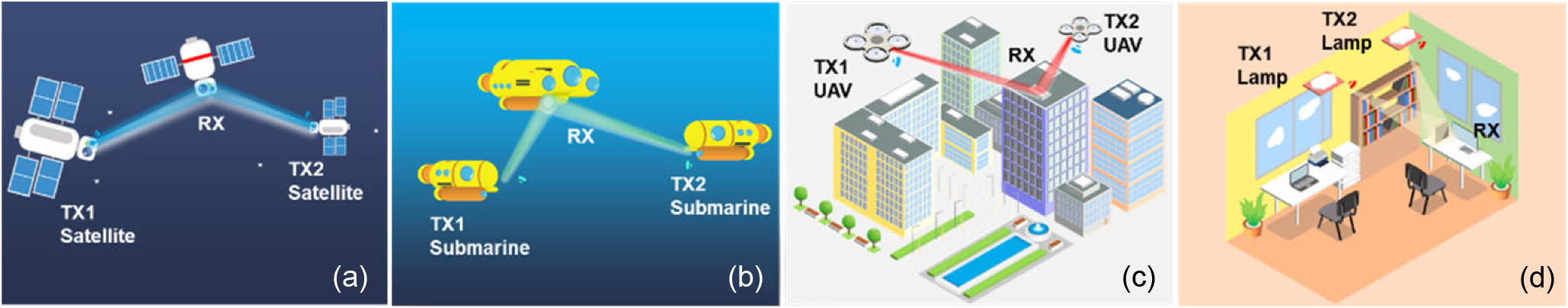
    Figure 1.Illustrations of the potential scenarios of superposed modulation in (a) satellite network VLLC, (b) underwater VLLC, (c) UAV and terrestrial VLLC, and (d) indoor VLLC.

    Therefore, multiple access VLC systems have become a heated research topic in recent studies. For example, MIMO-VLC systems based on indoor LED systems are intensively studied [1014]. Although such a system enables serving multiple users simultaneously and has a desirable compatibility with the indoor illumination system, they are restricted by transmission speed. The highest data rate reported as we know by writing this paper is 6.689 Gb/s [15]. The visible light laser communication (VLLC) system utilizing laser modules features a large channel capacity compared with its LED-based counterparts. A direct-modulated laser can easily produce over Gb/s data rate [1619], which could be further improved by introducing wavelength-division multiplexing (WDM) [2022] or coherent modulation. However, the majority of studies in VLLC focus on point-to-point, single-channel transmission, and few investigate the high capacity of laser-based MIMO-VLC systems [20,23]. Besides, the integrated photodetector (PD) array device is a blank area to explore. Compared with discrete PD device arrays, the integrated device has smaller sizes and consequently is more suitable to implement miniaturized MIMO systems.

    Photodetectors utilizing GaN-based materials have been gaining popularity in recent research. One of their merits includes, for example, wide (3.4 eV) and tunable bandgap, high carrier mobility [2000  cm2/(Vs)], and stronger robustness against harsh environments [24]. Moreover, the desirable responsivity in short-wavelength visible light signals, which include the blue-green transmission window [25] in underwater channels, is far from the responsivity peak of conventional commercialized PDs (Si-based: 1100  nm, for example). The existing research about GaN-based photodetectors now is intensively studied. Researchers explored multiple structures of such photodetectors, including metal-semiconductor-metal (MSM) structures [26,27], 2D structures (MXene GaN/InGaN) [2830], and multiple-quantum-wells (MQWs) [16,31,32]. Among them, research on MQWs structure demonstrates desirable data rate performance at the Gb/s level in existing studies [16,32]. In our previous studies, high-speed MQW devices have achieved over 10 Gb/s communication rates [33,34], suggesting that they have the potential to challenge commercialized PDs in the short-wavelength visible light spectrum, such as Si-based Thorlabs APD210 [35]. Compared with recently reported microarray structure devices, such as nano-hole [36], nano-wire [37,38], nano-tube [39], and planar structure [40] arrays, its detector-level array is more suitable to implement the multiple access function. And it has a durability advantage over organic detectors [41]. Hence, it is worth further investigation into its performance as a MIMO-VLC system. We listed these relavant research in Table 1 to demonstrate the highlight of the proposed device.

    In this paper, we demonstrate a flexible 2×2 multiple access visible light communication system based on an integrated parallel micro-PD array, which can provide access for two independent transmitters at the same time. It has a desirable dark current level and responsivity characteristics in the short-wavelength visible light spectrum. It implements a 2×2 visible light laser MIMO system using two photosensitive units and two independently driven 405 nm lasers. The highest data rate achieved with this multi-access system is 13.2 Gb/s, and the corresponding net data rate (NDR) achieved is 12.27 Gb/s after deducing the FEC overhead, using 2.2 GHz bandwidth and superposed PAM signals, when the channel condition is well-balanced. And the Huffman coding enables fine-grain, non-integer modulation order in the superposed MIMO system, and it significantly alleviates the decrease in the overall data throughput when user signal powers are extremely imbalanced. This experiment shows that this multi-access system can provide reliable high-speed access when the transmission distance, weather, or other channel conditions vary drastically. As far as we know, this is the first demonstration of multiple visible light laser source access based on a single integrated GaN/InGaN receiver module.

    2. DEVICE CHARACTERISTICS AND FABRICATION

    The array device is shown in Fig. 2. Figures 2(a) and 2(b) show the SEM image of the overall and detailed structure. The microscopic picture is shown in Fig. 2(c), which demonstrates the real appearance of the chip. The 16 detector units are first grouped by 4 in one row, and all rows are finally connected to the disk-shaped common cathode. The zoom-in image presents a detailed view of a single unit. The size of the unit is 50  μm×50  μm. The edge area of the unit is the passivation area that encloses the conductive materials in the center to reduce leakage current. The metal contact appears at the bottom of the image, which connects the unit to the common cathode. In Fig. 2(d), the layer structure of the chip is illustrated. The active regions including the 8 periods of MQWs are protected by the passivation shell. The layer nearest to the metal contact is Si-doped N-type GaN. The following structure is the In0.1Ga0.9N/GaN superlattice (SL) layer that helps to improve the quality of the MQWs. The period of the SL layer is 26. Besides, a layer of low-temperature (LT) GaN is placed before the MQWs to alleviate the strain in the material. The MQWs (In0.3Ga0.7N/GaN) are a crucial part of this device, whose bandgap design dictates the responsivity along the spectrum. After the Mg-doped P-type GaN, the last part of the vertical structure is the silver layer that reflects the incident light backward. This is a useful structure in LED design that improves light extraction as the backward emission comes out from the front side. For the same reason, the optical signal could be better utilized as the light that arrives at the bottom of the detector would return to the active layer. Figure 2(e) illustrates the exploded view of the micro-PD array. It highlights the common cathode and anode structure in this device, which means that all the 16 units are parallelly connected and the output of this device is the sum of the photo-generated current from all the detector units.

    (a) SEM images of the proposed micro-PD array. (b) The detailed SEM images of two detectors. (c) The optical microscopic image of the PD array chip. All cathodes on this chip are connected into the common cathode located at the center of the chip. (d) The intersection of a single detector unit, showing its layer structure. (e) The exploded view of the micro-PD array. The common N-node and the conduction substrate (the common anode) are illustrated.

    Figure 2.(a) SEM images of the proposed micro-PD array. (b) The detailed SEM images of two detectors. (c) The optical microscopic image of the PD array chip. All cathodes on this chip are connected into the common cathode located at the center of the chip. (d) The intersection of a single detector unit, showing its layer structure. (e) The exploded view of the micro-PD array. The common N-node and the conduction substrate (the common anode) are illustrated.

    There are two main features of this design. First, the V-pit structure within the MQWs has shown its enhancement to both the transmitter and receiver [34,42,43] in the VLC system. It facilitates carrier transportation, which increases the carrier recombination under forward bias voltage, and the extraction of photo-generated carriers when the reverse bias is applied. Second, the parallel connection collects the photocurrents from all the photo-sensitive areas. Signals in orthogonal dimensions can be simultaneously received and independently decoded. Therefore, this structure naturally superposed the signal as Fig. 3 shows.

    The 3D schematic diagram of the array device and how the independently received signals are superposed via the common cathode and anode structure.

    Figure 3.The 3D schematic diagram of the array device and how the independently received signals are superposed via the common cathode and anode structure.

    To demonstrate the device characteristics, we perform several device-level experiments. In Fig. 4, we first demonstrate the dark current measurement result. The measurement corresponds to the sum of all the dark currents in every detector unit of the array. According to Fig. 4(a), in the reversely biased region, the dark current level is below 1 μA level in most cases, and its current level falls dramatically beneath 1 nA when the reverse bias is higher than 5  V. When the bias current continues to increase, the device turns into an LED-like device, and the current surges to 1 mA. The low dark current level suggests a high signal quality as the dark current takes a negligible proportion when measuring the photocurrent. This advantage has already been studied in previous research [4446]. In these studies, it is discovered that the V-pit structure suppresses the formation of dislocations [45,46] and hence reduces the current leakage level by orders of magnitude [44]. Meanwhile, it also shows decent control of current leakage in the chip design and manufacturing process.

    (a) Dark current result measured with a Keithley 2450 source-meter. The dark current level could be lower than 1 nA. (b) The electroluminescence spectra measured using a spectroscope. (c) The normalized responsivities for two randomly selected units measured with a monochromator and calibrated using an optical power meter Newport 2936-R. The responsivity performance is highly identical between the units. (d), (e) The photocurrent measurement of the two selected units.

    Figure 4.(a) Dark current result measured with a Keithley 2450 source-meter. The dark current level could be lower than 1 nA. (b) The electroluminescence spectra measured using a spectroscope. (c) The normalized responsivities for two randomly selected units measured with a monochromator and calibrated using an optical power meter Newport 2936-R. The responsivity performance is highly identical between the units. (d), (e) The photocurrent measurement of the two selected units.

    Next, the electroluminescence spectrum is shown to present its spontaneous emission and bandgap design. The line chart shows the normalized intensity along the spectrum from 400 to 800 nm. According to the MQW design in bandgap, the emission peak wavelength should be at around 550–600 nm. Because a larger current bias means a higher applied voltage, the energy band structure would be distorted and cause a “blue shift” to the peak wavelength. The bandgap predicts the cutoff wavelength in absorption in Fig. 4(c).

    In the responsivity measurement, we randomly select two units of the 16 available ones. The photocurrent is recorded using a Keithley 2400 source meter. The light is from a Xe lamp and a Cornerstone 260 UV-VIS monochromator. The optical power is measured using a 2936-R optical power meter from Newport. The result shows two almost identical lines representing the responsivity of the selected units. The peak responsivity is located at 370 nm, as a modification to the device reported [33]. The response in the short-wavelength visible light spectrum is also significant. This part reflects the photocurrent generated by the MQWs, which slowly decreases as the wavelength rises from 400 to 550 nm. After 550 nm, the energy of the photon is no longer larger than the bandgap in the MQWs, and hence the response is cut off.

    The photocurrents of the selected two units are shown in Figs. 4(d) and 4(e). The two results are highly similar. When the bias current for the laser increases, the maximum photocurrent significantly enlarges, especially when the reverse bias is larger than 4  V. This suggests that higher reverse bias not only means a higher dark current but also a higher efficiency in converting the incident photon into free carriers, which means higher quantum efficiency and responsivity.

    3. PRINCIPLE AND EXPERIMENTAL SETUP

    A. Experiment Setup

    The setup used for this experiment is illustrated in Fig. 5. We apply an M8190 Keithley arbitrary waveform generator (AWG) to generate two independent data sequences using Mersenne Twister code to avoid predictable patterns within the data length. The two electric signals are later amplified by an electrical amplifier (EA, ZFL-2500VH+, 2.5 GHz bandwidth, 20 dB Gain). An attenuator is used to adjust the signal power, and its attenuation is fixed in the experiment. Next, the amplified signals are coupled with the DC component to bias the laser using a bias-T (Mini-Circuit AFBT-4R2GW-FT+). Two 405 nm lasers are used to produce the optical signal.

    The experiment setup schematic for the VLLC communication system with superposition modulation. The signals for in-phase and quadrature channels are independently generated from the same AWG and transmitted in two identical optical channels. The original scalar symbols finally form a 2D vectorial symbol at the receiver side.

    Figure 5.The experiment setup schematic for the VLLC communication system with superposition modulation. The signals for in-phase and quadrature channels are independently generated from the same AWG and transmitted in two identical optical channels. The original scalar symbols finally form a 2D vectorial symbol at the receiver side.

    The optical path is designed to converge the two laser beams and focus the beam onto two different units on the array device. The collimator on the laser, the convex lens, and the two sets of reflective mirrors in each branch of the optical path form a collimating system to control the beam spot size and the direction of the beam. The 20× objective lens is used to reduce the beam width and reduce the power wasted on the non-photosensitive area of the PD. The total light path is 65 cm, and the length after the beam splitter is 24 cm long.

    The PD is biased using a Keithley 2400 source meter, which is also used to measure the DC component in the photocurrent. It helps to tune the beam position by reading the photocurrent until the photocurrent measurement is at its maximum. When the two optical signals are received at the receiver, they simultaneously form a superposed signal. The superposed signal contains no DC component; therefore, it is later amplified by another ZFL-2500+ amplifier and finally received by the oscilloscope (OSC, Agilent DSA90604A).

    B. Superposition Modulation DSP

    The DSP process is shown in Fig. 6. It is a 2×2 MIMO system. First, the original uniformly distributed binary data sequences simulating the two users are converted into a set of probabilistically shaped, non-uniformly distributed PAM signals by a certain Huffman codebook. The symbols in each channel follow a certain dyadic distribution (the probability is 1/2, 1/4, 1/8 …), which can be acquired by mapping a uniformly distributed binary sequence using a specific Huffman codebook. In this experiment, we designed one Huffman-coded PAM4 (SE=1.75  bit/Hz) and two PAM8 (SE=2.75 and 2.875 bit/Hz). Note that not all Huffman codebooks have a symmetric tree structure, and therefore the originally encoded PAM signals may follow an asymmetry distribution with a non-zero mean value. To solve this problem, interleaving two coded PAM signals whose distribution is symmetrical to each other would result in the zero-valued mean of the transmitted PAM signal. And the signal distribution no longer follows dyadic distribution until the receiver deinterleaves the received symbols. Figure 6 shows the case when the I channel uses PAM8 and the Q channel uses PAM4. The PAM signals are prepared for the next SCM modulation step, including 4× upsampling, upconversion, and pulse-shaping filtering. The modulated time sample sequences are imported to the AWG, which generates two output (the in-phase and quadrature) AC signals for the optical channels.

    The DSP process for the communication system adopting superposition modulation enhanced by Huffman coding. By replacing conventional, integral-ordered QAM modulation with probabilistically shaped symbols, this system presents stronger flexibility and shaping gain in power utilization.

    Figure 6.The DSP process for the communication system adopting superposition modulation enhanced by Huffman coding. By replacing conventional, integral-ordered QAM modulation with probabilistically shaped symbols, this system presents stronger flexibility and shaping gain in power utilization.

    After the VLLC channel, in the OSC the two PAM signals are superposed orthogonally into a QAM symbol. However, unlike traditional QAM, its in-phase and quadrature dimensions can have different orders. The superposed signal exported from the OSC next experiences the rest of the DSP processes. The DSP process at the receiver side first synchronizes the signal waveform, and next, it applies waveform-level equalization to mitigate channel effects such as ISI and nonlinearity. Afterward, the program demodulates the waveform sample into two recovered PAM symbol sets. The two sets experience downsampling processes and symbol-level equalization to further reduce the channel effects. Next, the inverse process of Huffman encoding happens to decode the PAM result using the identical Huffman codebook to what the TX side uses. The results are used to calculate the BER performance separately. Only when the BER levels of both users are lower than 0.0038, the threshold for 7% HD-FEC, would the transmission process be acknowledged as valid.

    4. EXPERIMENTAL PERFORMANCE AND DISCUSSION

    A. Communication System Working Point

    First, we measure the photocurrent when placing the PD in the optical setup. The total photocurrent does not double the result of a single unit, but it remains the same level. This phenomenon is caused by the 50:50 beam splitter, which reduces the total optical power by half, and thus the photocurrent by two lasers is approximately the same as operating with one laser without the beam splitter. The maximum photocurrent appears when both the lasers are biased by 95 mA current. Cases with currents larger than 95 mA are not tested, as the laser might be damaged by large bias current. The gradient of the contour diagram in Fig. 7(a) suggests that the linearity around the maximum photocurrent is ideal, which indicates less nonlinearity in the superposed signal.

    (a) Photocurrent measurments in the communication system. Notice that the beam splitter in Fig. 5 causes a loss of half the photocurrent. (b), (c) The measured BER performance when only the in-phase or quadrature channel laser is turned on. (d) The system access information rate (AIR) performance when the peak-to-peak voltage (Vpp) is fixed when both lasers are turned on. (e) The AIR performance when the bias current of the laser is fixed while the Vpp is changing.

    Figure 7.(a) Photocurrent measurments in the communication system. Notice that the beam splitter in Fig. 5 causes a loss of half the photocurrent. (b), (c) The measured BER performance when only the in-phase or quadrature channel laser is turned on. (d) The system access information rate (AIR) performance when the peak-to-peak voltage (Vpp) is fixed when both lasers are turned on. (e) The AIR performance when the bias current of the laser is fixed while the Vpp is changing.

    Next, in Figs. 7(b) and 7(c) we measure the BER performance when only one of the lasers is transmitting optical signals. The bandwidth is 2.2 GHz, and the signal is modulated using PAM8 format. The results of the two lasers mainly differ in the best bias current due to the difference in laser package. The first unit operates at the best level when the bias current is 95 mA and the peak-to-peak voltage (Vpp) is at 700 mV. The BRE performance drastically decreases when the bias current for the laser reduces. The instantaneous power might damage the laser given that there are AC signals. The second laser works at approximately the same Vpp level, but the best bias current is 5 mA lower than that of the first laser. When opening the two lasers simultaneously, we test the best working point again in Figs. 7(d) and 7(e). When testing the influence of the bias current, we fix the Vpp at 700 mV. In general, the system performance is the best when both lasers are working at 95 mA bias current. Next, we vary the Vpp configuration when setting the bias currents at 95 mA for both lasers. It shows that the best Vpp does not change for both lasers. Therefore, we conclude that the best working point for the transmitters in the experiment system is 95/95 mA–700/700 mV.

    B. Huffman Coding Effect in Single Channel

    Following the investigation of the transmitter operating condition optimization, the next experiment compares the system performance when adjusting the reverse bias voltage, the magnitude of which is tuned from 0 V to 16 V. The line charts directly represent the communication performance measured using BER and mutual information (MI) to demonstrate the achievable information rate. The system performance generally improves as the amplitude of voltage bias is elevated. The reducing BER and rising MI suggest that the system is gaining larger channel capacity. The insets in the middle of Fig. 8 are the received PAM8 symbol distribution corresponding to each of the reverse biases. The histograms show that, at lower bias voltage, the 8 symbols are not distinctively divided into independent peaks, which means severe symbol error rates. But at higher bias voltages, the 8 peaks are separated. This phenomenon is attributed to the varying signal-to-noise ratio (SNR) under different bias voltages. The insets at the right part of Fig. 8 also support the conclusion that the spectra at lower bias voltages present a larger slope, causing a substantial power loss at higher frequencies. By contrast, the high-frequency spectra at larger bias voltages gain significant elevation, which helps increase the received signal power and reduces the signal distortion in frequency simultaneously. Although the rising bias also increases the dark current from sub-nA to μA level, it is worth trading the noise for a substantially improved 10  dB bandwidth from less than 600 MHz to 1200 MHz. The improved high-frequency response results in an increased signal power and overcomes the increment in noise. As a counter-intuitive result, the BER decreases when the noise level rises. Raising the bias further may continue this exponentially increased dark current and may start to exacerbate the BER performance. However, this may also cause permanent damage to this device. For safety concerns, we did not test bias voltages larger than 16 V and kept the bias at 16 V for the following experiment to ensure the best communication result.

    System performance when only the channel 1 (in-phase) or 2 (quadrature) laser is turned on. The system performance gradually improves when the reverse bias voltage is elevated. (a) The BER and achievable information rate (AIR) per symbol versus reverse voltage bias in channel 1. (b) The BER and AIR per symbol versus reverse voltage bias in channel 2. (c) The device dark current and the average measured −10 dB bandwidth of channels 1 and 2.

    Figure 8.System performance when only the channel 1 (in-phase) or 2 (quadrature) laser is turned on. The system performance gradually improves when the reverse bias voltage is elevated. (a) The BER and achievable information rate (AIR) per symbol versus reverse voltage bias in channel 1. (b) The BER and AIR per symbol versus reverse voltage bias in channel 2. (c) The device dark current and the average measured 10  dB bandwidth of channels 1 and 2.

    The next part of the experiment is the comparison between Huffman coding and a regular, uniformly distributed PAM signal in each one of the two channels. By controlling the peak-to-peak voltage, the received signal power changes from low to high. At low Vpp, the signal amplitude is too small, and the channel impairment is mainly the background noise. In high Vpp cases, the signal amplitude is too high and thus causes a nonlinear response in the system, which replaces the noise as the major factor of the negative channel effect. The result is shown in Fig. 9.

    First, we measured the BER performance of each coding scheme in the “noise-dominated” region. The highest BER appears in regular PAM8 format, which is closely followed by the first and second dyadic PAM8 coding (SE=2.875 and 2.75 bit/Hz). However, the three modulation formats utilizing the PAM8 constellation fail to meet the BER threshold when the Vpp is lower than 200 mV. PAM4 could work at 200 mV, and the Huffman coding scheme utilizing the same constellation could work at 141 mV Vpp. The symbol distribution insets in the two shaded A areas in Fig. 9 column A explain the reason that, due to channel noise, the PAM8 constellation does not have enough distance between the symbols like PAM4. The probabilistic shaping gain in PAM4 results in more distinctive peaks. When the Vpp is elevated, the signal power is increased to overcome the noise. However, when Vpp continues to rise, the BER performances of all the modulation formats gradually exacerbate. Different from noise, this impairment resulting from nonlinearity mainly affects the high-power symbol. The symbols located at the sides have larger signal power and hence are more vulnerable to nonlinear channel response. Comparing the insets corresponding to the shaded areas B and C, the first and the last peaks in C are spread wider, and the peaks become asymmetric, whose symbols are more distributed in areas closer to the center. In this case, Huffman-coded constellations demonstrate another advantage over regular PAM, that it has fewer high-power symbols susceptible to nonlinear channel effects. In the line chart, the dyadic distributed PAM again outperforms conventional PAM. The first and second dyadic PAM8 continue to work under the BER threshold until 1000 and 1400 mV Vpp, but conventional PAM8 fails to work between 1000 and 1100 mV.

    Relevant Research in III-Nitride-Based PDs

    DeviceRise/Fall TimeData RateDetector DimensionCommunication ModeRef.
    GaN/InGaN MSM93×93  μm[26]
    GaN/InGaN MSM23 ps2 μm (Gap spacing)[27]
    MXene/InGaN60/80 μs150×150  μm[28]
    MXene/GaN7.55 μs/1.67 ms3×5 array, 2  mm2 (total area)[29]
    MXene-GaN60 ms/20 ms2×2  μm[30]
    Semipolar InGaN/GaN MQWs540 Mb/s2×4 array, 30×30  μm (single unit)Point to point[31]
    InGaN/GaN MQWs3.2 Gb/s80×80  μmPoint to point[32]
    Semipolar InGaN/GaN MQWs7.4 Gb/s28.3  μm2Point to point[16]
    InGaN/GaN MQWs10.8 Gb/s4×4 array, 50×50  μm (single unit)Point to point[33]
    InGaN/GaN MQWs12.27 Gb/s4×4 array, 50×50  μm (single unit)2×2 MIMOThis work

    C. Huffman Coding Effect in MIMO Channel

    In the final communication experiment, we turned on both channels, whose performances are recorded. We applied two strategies in modulation: one only utilizes traditional PAM with integer modulation order, and the other can use dyadic PAM. The highest modulation order that satisfies the BER requirement is recorded and plotted in Fig. 9.

    System performance when Huffman coding is applied. (a) and (b) are the measured BER for channel 1. (c) and (d) show the BER for channel 2. (a) and (c) plot the BER in the low Vpp case using attenuators. (b) and (d) extend the Vpp to 1400 mV. The insets on the right side provide the histogram of the received symbols.

    Figure 9.System performance when Huffman coding is applied. (a) and (b) are the measured BER for channel 1. (c) and (d) show the BER for channel 2. (a) and (c) plot the BER in the low Vpp case using attenuators. (b) and (d) extend the Vpp to 1400 mV. The insets on the right side provide the histogram of the received symbols.

    The first channel is set at constant signal power to simulate a stable channel. At the same time, the second channel has a varying Vpp to resemble a channel with strong power fluctuation. For the first channel, its performance remains steady when the Vpp for channel 2 is lower than 800 mV. However, when the second channel gains larger power, the first channel is significantly influenced due to the interference from channel 2. The maximum usable modulation order, if not applying dyadic modulation and Huffman coding, would drop to 2 and even 1. By contrast, by Huffman coding, the usable maximum modulation order could decrease more slowly, able to operate at 2.85 and 2.75 bit/Hz before falling to 2 bit/Hz and 1.75 bit/Hz before finally using 1 bit/Hz. This could be attributed to the shaping gain and higher efficiency utilizing the SNR in Huffman coding and dyadic distribution. The condition in the second channel is different from the channel 1 case. It suffers from insufficient signal-to-noise level when channel 2 Vpp is low. But it also faces the challenge of channel nonlinearity when channel 2 Vpp is larger than 800 mV. Similarly, the maximum modulation order is improved in the low Vpp area because Huffman coding can utilize the SNR with higher efficiency, and the performance in the high-power area is also significantly elevated. This phenomenon is attributed to its robustness to nonlinearity as shown and discussed in the previous single-channel experiment.

    Combining the first and second diagrams in Fig. 10, the third diagram shows the total net data rate (NDR). The insets at the right side of the figure are the constellations corresponding to Fig. 1(c), whose color represents the distribution density. The superposed constellations vary from QAM8 to QAM64, and some demonstrate a probabilistic shaping effect, especially when the NDR slumps in regular PAM cases. The system performs the best when the channel 2 signal power is 73.5% to 131% of that in channel 1. The maximum rate is 13.2 Gb/s (6 bit/Hz, 2.2 GHz bandwidth). After deducting the overhead in 7% FEC, its NDR is 12.27 Gb/s. Either too small or too large of a signal in channel 2 would cause severely imbalanced channel conditions and exacerbate the total NDR performance significantly. But Huffman coding successfully improves the system performance in both noise-dominated and nonlinearity-dominated regions. Huffman coding mainly enhances the data rate of channel 1 in the noise-dominated region below 700 mV, improving the NDR by 1.53 Gb/s at 300 mV and 1.73 Gb/s at 550 mV Vpp. The system enters the nonlinearity-dominated region when channel 2 Vpp is above 700 mW, and the excess signal power affects both channels. When channel 2 increases its Vpp to 900 mV, using regular PAM formats loses 1/3 of the NDR, but by applying Huffman coding, the shaping gain increases the NDR by 3.48 Gb/s. The enhanced NDR means that Huffman coding can better resist the negative effect of the extremely unbalanced user signal power on the overall data throughput. To translate this result into the performance under varying received power, we measure the equivalent power gain corresponding to the Vpp at the transmitter in Fig. 10(d). It shows the real gain in signal power when tuning the Vpp. Combining Figs. 10(a)–10(c), we plot the working range of the system at each NDR. It demonstrates the advantage of Huffman-coded PAM over regular PAM in its robustness. The working range of Huffman-coded PAM leads regular PAM by 34.4% when the NDR is set at 12 Gb/s. The biggest gap appears at PAM=11  Gb/s, where Huffman coding increases the working range by 157%. However, in extreme cases, the advantage of Huffman-coded PAM reduces to 16.4%. This result suggests that the system with Huffman-coded PAM can provide more reliable transmission, alleviating the rate loss caused by the received power variation, which may be caused by changes in communication distance, weather, or turbulences in the channel.

    Control of the Vpp of channel 1 at 700 mV. The comparison between the system performance with or without Huffman coding and variation of the Vpp of channel 2. (a) The net data rate after deducting the FEC overhead (NDR) of channel 1. (b) The NDR of channel 2. (c) The total NDR and the constellation diagrams corresponding to each Vpp. (d) The equivalent power gain of Vpp. (e) Comparing the Vpp working range in mV versus NDR when using regular PAM or Huffman-coded PAM.

    Figure 10.Control of the Vpp of channel 1 at 700 mV. The comparison between the system performance with or without Huffman coding and variation of the Vpp of channel 2. (a) The net data rate after deducting the FEC overhead (NDR) of channel 1. (b) The NDR of channel 2. (c) The total NDR and the constellation diagrams corresponding to each Vpp. (d) The equivalent power gain of Vpp. (e) Comparing the Vpp working range in mV versus NDR when using regular PAM or Huffman-coded PAM.

    5. CONCLUSION

    In this paper, we demonstrate an integrated parallel micro-PD array device that can support two different users transmitting independent signals simultaneously. It has a desirable dark current level and responsivity characteristics in the short-wavelength visible light spectrum. It implements a 2×2 visible light laser MIMO system using two photosensitive units and two independently driven 405 nm lasers. Using 2.2 GHz bandwidth, the maximum rate achieved is 13.2 Gb/s, and its corresponding net data rate (NDR) is 12.27 Gb/s, after deducting the FEC overhead. And the Huffman coding enables fine-grain, non-integer modulation order in the superposed MIMO system, and it significantly alleviates the decrease in the overall data throughput when user signal powers are extremely imbalanced. This experiment shows that this multi-access system can provide reliable high-speed access when the transmission distance, weather, or other channel conditions vary drastically. As far as we know, this is the first demonstration of multiple visible light laser source access based on a single integrated GaN/InGaN receiver module.

    References

    [1] N. Chi, Y. Zhou, Y. Wei. Visible light communication in 6G: advances, challenges, and prospects. IEEE Veh. Technol. Mag., 15, 93-102(2020).

    [2] H. Sharma, R. K. Jha. VLC enabled hybrid wireless network for B5G/6G communications. Wireless Pers. Commun., 124, 1741-1771(2022).

    [3] M. Z. Chowdhury, Md. Shahjalal, S. Ahmed. 6G wireless communication systems: applications, requirements, technologies, challenges, and research directions. IEEE Open J. Commun. Soc., 1, 957-975(2020).

    [4] B. Ali, M. A. Gregory, S. Li. Multi-access edge computing architecture, data security and privacy: a review. IEEE Access, 9, 18706-18721(2021).

    [5] M. Poongudi, S. Bourouis, A. N. Ahmed. A novel secured multi-access edge computing based VANET with neuro fuzzy systems based blockchain framework. Comput. Commun., 192, 48-56(2022).

    [6] K. Liolis, A. Geurtz, R. Sperber. Use cases and scenarios of 5G integrated satellite-terrestrial networks for enhanced mobile broadband: the SaT5G approach. Satell. Commun. Netw., 37, 91-112(2019).

    [7] G. E. Burrowes, J. Brown, J. Y. Khan. Adaptive space time—time division multiple access (AST-TDMA) protocol for an underwater swarm of AUV’s. MTS/IEEE OCEANS—Bergen, 1-10(2013).

    [8] O. Bello, S. Zeadally. Internet of underwater things communication: architecture, technologies, research challenges and future opportunities. AdHoc Netw., 135, 102933(2022).

    [9] Q. Wang, Y. Liu, V. G. Menon. UAV-enabled non-orthogonal multiple access networks for ground-air-ground communications. IEEE Trans. Green Commun. Netw., 6, 1340-1354(2022).

    [10] M. A. S. Sejan, M. H. Rahman, M. A. Aziz. A comprehensive survey on MIMO visible light communication: current research, machine learning and future trends. Sensors, 23, 739(2023).

    [11] Z. Gao, Y. Wang, X. Liu. FFDNet-based channel estimation for massive MIMO visible light communication systems. IEEE Wireless Commun. Lett., 9, 340-343(2020).

    [12] L. An, H. Shen, J. Wang. Energy efficiency optimization for MIMO visible light communication systems. IEEE Wireless Commun. Lett., 9, 452-456(2020).

    [13] N. Su, E. Panayirci, M. Koca. Physical layer security for multi-user MIMO visible light communication systems with generalized space shift keying. IEEE Trans. Commun., 69, 2585-2598(2021).

    [14] W. Niu, Z. Xu, W. Xiao. Phosphor-free golden light LED array for 5.4-Gbps visible light communication using MIMO Tomlinson-Harashima precoding. J. Lightwave Technol., 40, 5031-5040(2022).

    [15] J. Shi, Y. Liu, Z. Luo. Simplified neural network with physics-informed module in MIMO visible light communication systems. J. Lightwave Technol., 42, 57-68(2023).

    [16] O. Alkhazragi, C. H. Kang, M. Kong. 7.4-Gbit/s visible-light communication utilizing wavelength-selective semipolar micro-photodetector. IEEE Photon. Technol. Lett., 32, 767-770(2020).

    [17] G. Qin, Q. Biau, W. Niu. 100 m free-space visible light communication at 6 Gbps GS-APSK modulation utilizing a GaN blue LD. Asia Communications and Photonics Conference (ACP), 1-3(2021).

    [18] J. Hu, F. Hu, G. Li. A 15 Gbps 520-nm GaN laser diode based visible light communication system utilizing adaptive bit loading scheme. IEEE 6th Optoelectronics Global Conference (OGC), 31-34(2021).

    [19] L.-Y. Wei, Y. Liu, C.-W. Chow. 6.915-Gbit/s white-light phosphor laser diode-based DCO-OFDM visible light communication (VLC) system with functional transmission distance. Electron. Lett., 56, 945-947(2020).

    [20] W. H. Gunawan, C.-W. Chow, Y. Liu. Optical beam steerable visible light communication (VLC) system supporting multiple users using RGB and orthogonal frequency division multiplexed (OFDM) non-orthogonal multiple access (NOMA). Sensors, 22, 8707(2022).

    [21] H. Pahuja, S. Sachdeva, M. Sindhwani. Capacity enhancement of WDM visible light communication system employing 3-SOPs/channel/LD color. J. opt. Commun.(2022).

    [22] J. Hu, F. Hu, J. Jia. 46.4 Gbps visible light communication system utilizing a compact tricolor laser transmitter. Opt. Express, 30, 4365-4373(2022).

    [23] A. Sharma, K. Singh, J. Malhotra. High speed 60 Gbps RGB laser based-FSOC link by incorporating hybrid PDM-MIMO scheme for indoor applications. J. Opt. Commun.(2023).

    [24] K.-T. Ho, R. Chen, G. Liu. 3.2 gigabit-per-second visible light communication link with InGaN/GaN MQW micro-photodetector. Opt. Express, 26, 3037-3045(2018).

    [25] G. S. Spagnolo, L. Cozzella, F. Leccese. Underwater optical wireless communications: overview. Sensors, 20, 2261(2020).

    [26] Y.-K. Su, Y.-Z. Chiou, F.-S. Juang. GaN and InGaN metal-semiconductor-metal photodetectors with different Schottky contact metals. Jpn. J. Appl. Phys., 40, 2996(2001).

    [27] J. C. Carrano, T. Li, D. L. Brown. Very high-speed metal-semiconductor-metal ultraviolet photodetectors fabricated on GaN. Appl. Phys. Lett., 73, 2405-2407(1998).

    [28] D. Kong, T. Lin, J. Chai. A self-powered MXene/InGaN van der Waals heterojunction mini-photodetector for visible light communication. Appl. Phys. Lett., 122, 142104(2023).

    [29] W. Song, J. Chen, Z. Li. Self-powered MXene/GaN van der Waals heterojunction ultraviolet photodiodes with superhigh efficiency and stable current outputs. Adv. Mater., 33, 2101059(2021).

    [30] C. Yi, Y. Chen, Z. Kang. MXene-GaN van der Waals heterostructures for high-speed self-driven photodetectors and light-emitting diodes. Adv. Electron. Mater., 7, 2000955(2021).

    [31] Y.-H. Chang, T.-C. Hsu, F.-J. Liou. High-bandwidth InGaN/GaN semipolar micro-LED acting as a fast photodetector for visible light communications. Opt. Express, 29, 37245-37252(2021).

    [32] K.-T. Ho. 3.2 gigabit-per-second visible light communication link with InGaN/GaN MQW micro-photodetector. Opt. Express, 26, 3037-3045(2018).

    [33] J. Shi, Z. Xu, W. Niu. Si-substrate vertical-structure InGaN/GaN micro-LED-based photodetector for beyond 10  Gbps visible light communication. Photon. Res., 10, 2394-2404(2022).

    [34] Z. Xu, Z. Luo, X. Lin. 15.26 Gb/s Si-substrate GaN high-speed visible light photodetector with super-lattice structure. Opt. Express, 31, 33064-33076(2023).

    [35] X. Liu, S. Yi, X. Zhou. 34.5  m underwater optical wireless communication with 2.70  Gbps data rate based on a green laser diode with NRZ-OOK modulation. Opt. Express, 25, 27937-27947(2017).

    [36] A. Dubey, R. Mishra, Y.-H. Hsieh. Aluminum plasmonics enriched ultraviolet GaN photodetector with ultrahigh responsivity, detectivity, and broad bandwidth. Adv. Sci., 7, 2002274(2020).

    [37] M.-S. Jo, H.-J. Song, B.-J. Kim. Aligned CuO nanowire array for a high performance visible light photodetector. Sci. Rep., 12, 2284(2022).

    [38] A. Aiello, A. K. M. H. Hoque, M. Z. Baten. High-gain silicon-based InGaN/GaN dot-in-nanowire array photodetector. ACS Photon., 6, 1289-1294(2019).

    [39] A. M. Elsayed. Preparation and characterization of a high-efficiency photoelectric detector composed of hexagonal Al2O3/TiO2/TiN/Au nanoporous array. Mater. Sci. Semicond. Process., 139, 106348(2022).

    [40] Z. Xu, Y. Li, X. Liu. Highly sensitive and ultrafast responding array photodetector based on a newly tailored 2D lead iodide perovskite crystal. Adv. Opt. Mater., 7, 1900308(2019).

    [41] N. Ahn, M. Choi. Towards long-term stable perovskite solar cells: degradation mechanisms and stabilization techniques. Adv. Sci., 11, 2306110(2024).

    [42] Z. Xu, W. Niu, Y. Liu. 31.38  Gb/s GaN-based LED array visible light communication system enhanced with V-pit and sidewall quantum well structure. Opto-Electron. Sci., 2, 230005(2023).

    [43] F. Hu, S. Chen, Y. Zhang. High-speed visible light communication systems based on Si-substrate LEDs with multiple superlattice interlayers. PhotoniX, 2, 16(2021).

    [44] J. Kim, J. Kim, Y. Tak. Effect of V-shaped pit size on the reverse leakage current of InGaN/GaN light-emitting diodes. IEEE Electron Device Lett., 34, 1409-1411(2013).

    [45] K. Koike, S. Lee, S. R. Cho. Improvement of light extraction efficiency and reduction of leakage current in GaN-based LED Via V-pit formation. IEEE Photon. Technol. Lett., 24, 449-451(2012).

    [46] J. Park, J.-S. Ha. Reduction of leakage current in InGaN-based LEDs with V-pit embedded structures. J. Korean Phys. Soc., 60, 1367-1370(2012).

    Zengyi Xu, Xianhao Lin, Zhiteng Luo, Qianying Lin, Jianli Zhang, Guangxu Wang, Xiaolan Wang, Fengyi Jiang, Ziwei Li, Jianyang Shi, Junwen Zhang, Chao Shen, Nan Chi. Flexible 2 × 2 multiple access visible light communication system based on an integrated parallel GaN/InGaN micro-photodetector array module[J]. Photonics Research, 2024, 12(4): 793
    Download Citation