
Greta Merkininkaitė, Edvinas Aleksandravičius, Mangirdas Malinauskas, Darius Gailevičius, Simas Šakirzanovas. Laser additive manufacturing of Si/ZrO2 tunable crystalline phase 3D nanostructures[J]. Opto-Electronic Advances, 2022, 5(5): 210077
- Opto-Electronic Advances
- Vol. 5, Issue 5, 210077 (2022)
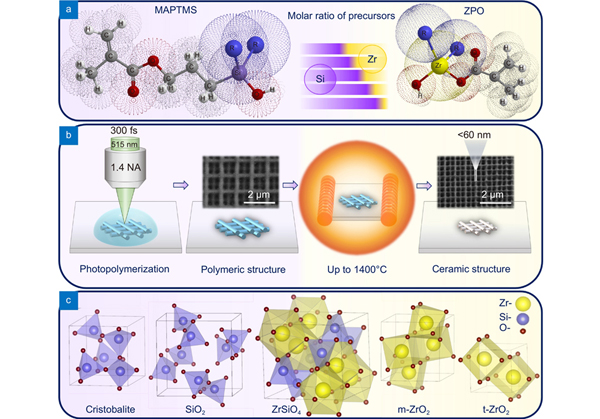
Fig. 1. Graphical abstract showing precursors, their molar ratios in (a ) syntheses, (b ) photopolymerization and calcination technology and (c ) formed crystalline phase lattices after calcination (Cristobalite, SiO2, ZrSiO4, monoclinic ZrO2 and tetragonal ZrO2). These phases can be observed depending on the treatment temperature and initial hybrid materials compositions.
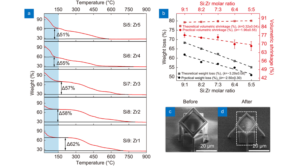
Fig. 2. (a ) TGA data of SiX:ZrY showing weight loss vs. temperature (red line). (b ) Theoretical (square symbols) and practical (circle symbols) weight loss for the phase transition from the polymeric to the glass/ceramic phase (black) and volumetric shrinkage (red) (theoretical- square symbols, practical- circle symbols) of cubes at the same phase transition (error bars of volumetric shrinkage represent Std. dev., n = 3, TGA measurements were performed once for each material, so it is not possible to include error bars for the weight loss). SEM images of the Si7:Zr3 cube before (c ) and after (d ) heat treatment at 1000 °C.
Fig. 3. Si9:Zr1 woodpiles (a –c ) before heat treatment and (d –f ) after heating at 1000 °C under air atmosphere. (a, d) Woodpiles fabricated at 200 μm/s speed (on the top line) and at 500 μm/s speed (on the bottom line) with 48, 56, 64 μW incident irradiation power. (b, c, e, and f) The highest resolution of woodpiles was obtained by applying 200 μm/s and 64 μW parameters. (g ) The dependence of Si9:Zr1, Si7:Zr3, Si5:Zr5 woodpiles lines width on the laser irradiance at 200 μm/s speed. Before heat treatment- solid lines, after- dashed lines. (h ) The dependence of Si9:Zr1, Si7:Zr3, Si5:Zr5 woodpiles lines width on the laser irradiance at 500 μm/s speed (error bars represent Std. dev., n = 3).
Fig. 4. X-ray diffractograms of structures (SEM images) annealed at 1000 °C (a-Si5:Zr5, b-Si6:Zr4, c-Si7:Zr3, d-Si8:Zr2, e-Si9:Zr1, f-reference data) and X-ray diffractograms of powders annealed at 1000 °C (g-Si5:Zr5, h-Si6:Zr4, i-Si7:Zr3, j-Si8:Zr2, k-Si9:Zr1, l-reference data). SEM images show corresponding 3D scaffolds treated at 1000 °C. SEM images correspond to the same scale bar.
Fig. 5. X-ray diffractograms of structures (SEM images) annealed at 1200 °C (a-Si5:Zr5, b-Si6:Zr4, c-Si7:Zr3, d-Si8:Zr2, e-Si9:Zr1, f-reference data) and X-ray diffractograms of powders annealed at 1200 °C (g-Si5:Zr5, h-Si6:Zr4, i-Si7:Zr3, j-Si8:Zr2, k-Si9:Zr1, l-reference data). SEM images show corresponding 3D scaffolds treated at 1200 °C temperature. SEM images correspond to the same scale bar.
Fig. 6. X-ray diffractograms of structures (SEM images) annealed at 1400 °C (a-Si5:Zr5, b-Si6:Zr4, c-Si7:Zr3, d-Si8:Zr2, e-Si9:Zr1, f-reference data) and X-ray diffractograms of powders annealed at 1400 °C (g-Si5:Zr5, h-Si6:Zr4, i-Si7:Zr3, j-Si8:Zr2, k-Si9:Zr2, l-reference data). SEM images show corresponding 3D scaffolds treated at 1400 °C temperature. SEM images correspond to the same scale bar.
Fig. 7. X-ray diffraction measurements. (a ) X-Ray diffraction pattern of Si6:Zr4 structure annealed at 1200 °C temperature. (b ) Reference patterns. (c ) Debye-Scherrer rings obtained after X-ray diffraction measurement. (d ) Photograph of Si6:Zr4 structure annealed at 1200 °C temperature before measurement.

Set citation alerts for the article
Please enter your email address
© Copyright 2018-2021 | Chinese Laser Press. All Rights Reserved 沪ICP备15018463号-20