Ion sensitive field effect transistor (ISFET) devices are highly accurate, convenient, fast and low-cost in the detection of ions and biological macromolecules, such as DNA molecules, antibodies, enzymatic substrates and cellular metabolites. For high-throughput cell metabolism detection, we successfully designed a very large-scale biomedical sensing application specific integrated circuit (ASIC) with a 640 × 640 ISFET array. The circuit design is highly integrated by compressing the size of a pixel to 7.4 × 7.4μm2 and arranging the layout of even and odd columns in an interdigital pattern to maximize the utilization of space. The chip can operate at a speed of 2.083M pixels/s and the dynamic process of the fluid flow on the surface of the array was monitored through ion imaging. The pH sensitivity is 33 ± 4 mV/pH and the drift rate is 0.06 mV/min after 5 h, indicating the stability and robustness of the chip. Moreover, the chip was applied to monitor pH changes in CaSki cells metabolism, with pH shifting from 8.04 to 7.40 on average. This platform has the potential for continuous and parallel monitoring of cell metabolism in single-cell culture arrays.Ion sensitive field effect transistor (ISFET) devices are highly accurate, convenient, fast and low-cost in the detection of ions and biological macromolecules, such as DNA molecules, antibodies, enzymatic substrates and cellular metabolites. For high-throughput cell metabolism detection, we successfully designed a very large-scale biomedical sensing application specific integrated circuit (ASIC) with a 640 × 640 ISFET array. The circuit design is highly integrated by compressing the size of a pixel to 7.4 × 7.4μm2 and arranging the layout of even and odd columns in an interdigital pattern to maximize the utilization of space. The chip can operate at a speed of 2.083M pixels/s and the dynamic process of the fluid flow on the surface of the array was monitored through ion imaging. The pH sensitivity is 33 ± 4 mV/pH and the drift rate is 0.06 mV/min after 5 h, indicating the stability and robustness of the chip. Moreover, the chip was applied to monitor pH changes in CaSki cells metabolism, with pH shifting from 8.04 to 7.40 on average. This platform has the potential for continuous and parallel monitoring of cell metabolism in single-cell culture arrays.
1. Introduction
Measurements of cellular metabolism are essential for understanding cancer, aging, cardiovascular and neurodegenerative diseases[1]. In particular, cancer cells inhibit oxidative phosphorylation in mitochondria and produce adenosine triphosphate (ATP) via glycolysis, allowing them to proliferate and metastasize in the absence of apoptosis[2]. The dissolution of cellular metabolites such as lactic acid[3] or carbon dioxide in a liquid environment results in a change in pH, which can be a useful indicator for characterizing cellular metabolism[4]. Optical and classic three-electrode systems have been used for detecting pH values around cancer cells. Although the optical method achieves high sensitivity using pH-sensitive fluorophores[5], it requires expensive optical equipment, such as microscopes, flow cytometers, or microplate readers[6]. Compared to the optical method, the three-electrode system converts electrochemical signals directly into potential and current signals for measurement[7], thereby reducing cost. However, it is limited by the production process of three electrodes, which are made from multiple kinds of materials and is difficult to be integrated with auxiliary circuits on a very large scale[8].
To address these issues, ion sensitive field effect transistor (ISFET) based on the metal–oxide–semiconductor field-effect transistor (MOSFET) has been proposed for pH sensing[9]. The biochemical signal of the analyte can be converted to electrical signals by a transducer according to potential, current, or impedance output of the ISFET, and transmitted to a signal analysis terminal via peripheral circuitry[10]. Optimized ISFET can be used to detect analytes such as ions, proteins, DNA molecules[11], etc., through different structures and sensitive materials of the gate[12]. Although ISFETs offer the advantages of speed, convenience, and low-cost, single ISFET is not suitable for high-throughput biochemical applications such as DNA sequencing[13,14], DNA amplification[15,16], and cell metabolism[17,18]. Biomedical sensing application specific integrated circuit (ASIC) with a large-scale ISFET array provides a high spatial and temporal resolution to solve these issues successfully[13-18]. Moreover, it is compatible with the standard complementary metal–oxide–semiconductor (CMOS) manufacturing process[19].
Here, we designed a cell metabolism detection ASIC including a very large-scale ISFET array, readout circuits, row and column selection registers, bias and source correlation circuits. According to the standard CMOS fabrication process, the top material of the passivation layer (Si3N4) was used as a transducer for exchanging hydrogen ions with the electrolyte. The spatial resolution of ion imaging was improved by designing the size of each pixel and a dynamic process of the fluid flow on the surface of the array was ion imaged. To evaluate the performance of the chip, sensitivity and drift were obtained by measuring buffers with different pH values. In addition, we measured that the pH of CaSki cell culture media decreased over three days, which is the result of lactic acid and hydrogen ion release caused by metabolism through the glycolysis pathway in cancer cells.
2. Experimental
2.1. ISFET fundamentals
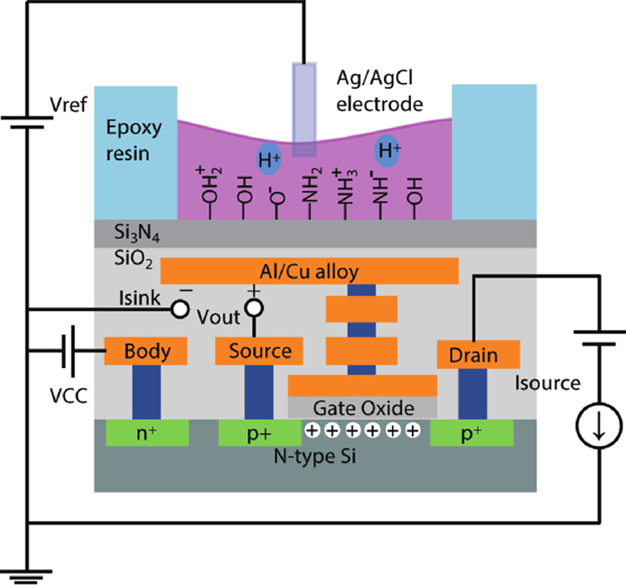
As shown inFig. 1, the structure of an ISFET is typically a combination of a conventional MOSFET, an electrolyte reservoir, and a referenc electrode (RE) that will provide a reference voltage to the electrolyte. The passivation layer of Si3N4, including amphoteric SiOH sites and basic SiNH2 sites on the surface, serves as a hydrogen ions sensing layer for ISFETs. There is a potential difference at the interface between the electrolyte and sensing layer and the potential difference is linearly correlated with the hydrogen ion concentration with a theoritical maximum of 59.2 mV/pH at standard room temperature[20]. The interface potential is then coupled to the top metal layer to drive the device work.
Figure 1.(Color online) Schematic cross-section of a p-type ISFET.
The interface potential is part of the threshold voltage (VTH) of an ISFET and in turn the drain–source current (IDS) is a function of this potential difference. Assuming that a p-type ISFET operates in the linear region, the formula should be[10]
whereµp is the mobility of charge carriers in the MOSFET,COX is the oxide capacity per unit area, andW andL are the gate width and length,VDS is the drain–source voltage, respectively. And the voltage at the source terminal can be calculated as
Therefore, the change inVTH can be reflected inVS, which is also theVout of the readout circuit.
2.2. ISFET array design
The readout circuit is presented inFig. 2(a). There are totally 5 modules: Pixel, Current source (Isource), Current sink (Isink), Amplifier A1, and Amplifier A2, where Isource, Isink and Amplifiers are controlled by the bias-voltage of Bias1, Bias2, and Bias3 respectively.
Figure 2.(Color online) Circuits and layout design of the chip. (a) The basic readout circuit of a unit. (b) Circuit diagram of the array. Although the odd and even columns are geometrically crossed and closed to each other, they are logically separated. The signals of the odd and even columns are sent to Vout1 and Vout2 terminals through the upper and lower electrical channels, respectively. (c) Pixels and readout circuit design of one column. (d) A top view of the chip layout.
To achieve maximum integration, each pixel in this chip consists of only 3 PMOS transistors, with the gate of one transistor keeps floating (Fig. 2(a)). This transistor operates as the ISFET, while the other two transistors work as switches and control the top source and the output route. The reason we selected PMOS is that it has lower noise than NMOS. In addition, by using PMOS transistors, doping of both substrates can be avoided, which is advantageous when maintaining a uniform body voltage. Since the designed pixel requires only three transistors, its area can be compressed. In this chip, each pixel was surrounded by a ring of contacts in order to provide a stable and uniform body voltage to the transistors. The area of this pixel was thus 7.4 × 7.4μm2[21], which can be reduced furtherly by a more advanced foundry process.
To achieve better speed performance, a basic single-stage amplifier structure was used in this chip. As depicted in module Amplifier A1 and Amplifier A2 ofFig. 2(a), the output signal was mirrored to the drain terminal of two current source transistors, which increased its voltage swing of output without introducing much parasitic capacitance effect.
To utilize the area more efficiently while achieving the best layout route, the odd and even columns of readout circuits were separated (Fig. 2(b)), and the corresponding circuits were placed either at the top (odd columns) or bottom (even columns) of the core area of the layout (Figs. 2(c) and2(d)). According to the circuit design shown inFig. 2(b), there will need to be at least three operational amplifiers for each column, for a total of 1920 operational amplifiers. It is extremely challenging to place so many amplifiers neatly in a limited space without compromising electrical properties. Multiple amplifiers should be in located close to the pixels so that the output channel can keep the shortest path. But the amplifiers also should not be compressed to an so narrow shape that the performance is destroyed. We thus arranged the amplifiers in a rectangle with a width of 14.8μm, which is twice the length of one pixel side. The layout of odd columns and even columns were then tightly arranged in an interdigital pattern. Through the elaborated design of pixels, amplifiers, and layout, nearly 1.5 million transistors were successfully integrated into a chip that maintains the optimal electrical performance.Fig. 2(d) is the layout of the whole integrated chip.
According to the basic electrical properties of PMOS, the electrolyte should be stabilized at a low voltage by an Ag/AgCl RE. The voltage value at the source of the ISFET, which is also the output of amplifier A2, should vary around half value of supply voltage (3.3 V) to obtain the best voltage swing. The ISFET is mainly operated in the linear region so that the potential of the drain terminal will not have to be close to the Gate terminal. The resistor, R, and current sink, Isink, guarantee that theVDS of the ISFET remains constant so that there is a direct correspondence between the output signal,Vout, and the floating gate voltage. In a real environment, the floating gate voltage is influenced by characteristics of the electrolyte, such as the pH that we will study in this paper. Hence, the output voltage can be used to characterize the electrochemical properties straightly. Otherwise, the current source and the current sink are just two current mirrors whose bias voltage generation depends on the regulation of the voltage applied to a resistor[22].
The gates of the ISFET sensors in the outermost circle and the second outermost circle of the array were connected and linked to two PADs, respectively. Two PAD terminals can provide different gate voltages to simulate the chemical signals. These two square circles help to verify the basic electrical properties of the chip and address the locations of the pixels.
2.3. Fabrication, encapsulation, and test
The 640 × 640 ISFET array chip was fabricated on a 4-metal 2-poly layer using a standard 0.35μm CMOS process from the Central Semiconductor Manufacturing Company (CSMC). The operating voltage of the standard library components is 3.3 V. The complete circuits occupy an area of approximately 9.3 × 8.7 mm2, with a sensing area of 4.736 × 4.736 mm2 (Fig. 3(b)). The chip has 53 PADs and is packaged in a Quad Flat Package (QFP) shell (Fig. 3(a)).Fig. 3(c) shows a 200× magnification micrograph of some pixels. The passivation layer consists of a 1.1µm oxide layer and a 0.7µm silicon nitride film on top of it (Fig. 3(d)).
Figure 3.(Color online) Images of the ISFET array after encapsulation and welding. Regions outlined with boxes of different colors were displayed in the figures of the corresponding colors. (a) Image of the chip encapsulated in a QFP shell. (b) Details of the chip. It includes a pixel array (middle), readout circuits and column selection circuits (top and bottom), and row selection registers (left). (c) A small portion of the pixel array was imaged under a microscope. Each pixel is 7.4 × 7.4µm2. (d) The SEM micrograph of the passivation layer. The top layer Si3N4 is used as the sensing layer.
To test the performance of the chip, we built a system consisting of a field programmable gate array (FPGA) as a clock circuit and a 16 bits data acquisition unit (DAQ) that collects electrical signals. The sampling clock of the DAQ unit and selection clock for the array were synchronized. Data is transferred serially and continuously to a host computer, which then converts the serial data to array format. The DAQ has six 16-bits ADC channels, and they all have a precision of 228μV, which means it’s sufficient to detect very weak electrochemical signals.
In preparation of the pH buffers employed in experiments, 0.1 M NaCl solution was used as the solvent, and NaOH and HCl were used to adjust the pH of the electrolyte. We used this combination of solvent and buffers to ensure that only two kinds of salt ions (Na+ and Cl−) were present in the electrolyte, and other ions, such as potassium, did not interfere with the operation of the device. The electrolyte buffers were prepared at 6 different pH values: 2.79, 4.36, 6.20, 9.50, 10.89, and 12.02. Commercial buffers were also prepared for some test requirements like the buffers need to be maintained at an absolutely stable pH value or calibrate the chip.
3. Results and discussion
3.1. Device characterization
To remove the trapped charge, the chip was exposed to ultraviolet (UV) light for 114 h prior to electrolyte detection according to the method introduced in a Ref. [23]. Then the output signals became flat before pixels contacted the electrolyte (Fig. 4(a)). A cylindrical pool was glued on the surface of the chip, forming a reservoir to inject sample and isolate it from the chip’s bonding wires. The area outside the reservoir was covered by epoxy resin. The output signals changed immediately when a sample was injected into the reservoir and the signal changes lies within a distinct circle outlining the boundary (Fig. 4(b)). The pH of the electrolyte was sensed by the pixels and converted to electrical signals by the readout circuits. The other pixels that were protected by epoxy resin bonder maintained a relatively high voltage. The output voltage varied between 0.9 and 2.8 V during the test.
Figure 4.(Color online) Signals of the ISFET array. (a) Initial signals of the ISFET array after UV irradiation with a reference voltage of 0 V. (b) Signal values decreased when the reference voltage was regulated to –4.0 V.
The fastest operational speed of the chip was investigated and the value is 2.083M pixels/s, which corresponds to about 31 frames/s. However, subject to the acquisition speed of DAQ and data analysis capability of computers, the scanning and acquiring speed was set as 160k pixels/s (0.78 frames/s) in this work. It would generate about 1G Bytes of data per minute at this speed.
3.2. Liquid flow process imaging
To further characterize the performance of the chip, the flow process of a volume of 20µL liquid on the surface of the ISFET array was imaged (Fig. 5). The acquisition interval of images was 1.28 s. Commercial buffer at pH = 7.00 was used to be test fluid. The output signals of all pixels were at a uniform voltage at first. Once the buffer comes into contact with the sensitive pixels, the electrical signal changes rapidly. As aforementioned, the signal will change to be near 1.65 V. The fluid flowed onto all sensitive pixels after 6.40 s, and the output signals were almost identical to each other.
Figure 5.(Color online) Ion imaging of dynamic flow process. (a) All sensitive pixels had uniform signals initially. (b–e) Once the buffer was injected into the chip, signals of the pixels in contact with the buffer changed immediately. (f) The buffer was evenly distributed across the surface, so each pixel had a similar output signal.
To verify the sensitivity of the device, the voltage of the RE was eventually maintained at approximately –4.0 V and buffers of different pH values were sequentially injected into the reservoir for testing, during which a washing process was also included. The output signals decreased linearly with increasing pH (Fig. 6(a)). After a linear fit made to the signals and pH values, the calculated slope of the curve represented the sensitivity of the ISFET sensors. The sensitivity was 33 ± 4 mV/pH (Fig. 6(b)), which was comparable to the sensitivity of many reported works[16,24,25]. The drift performance has also been measured, with a rate of –3 mV/min during the first two hours and –0.06 mV/min after 5 h. The drift rate also can be described as 0.09 pH/min at the first two hours and 0.002 pH/min after 5 h.
Figure 6.(Color online) (a) Voltage signals of six pH values for 1000 pixels. Each of the 1000 pixels was picked from the array per 20 rows and 20 columns, which could ensure the pixels were uniformly distributed. Each step is 20 acquired data in about 25 s, and the washing time is not included. The 20 acquired data were averaged to calculate the pH sensitivity of a pixel. (b) The pH-to-output voltage curve for the same pixels in (a). Each point is the mean value of the pixels, and the error bar is also calculated from the data.
Commercial buffers of different pH values were repeatedly tested for three times. There was no significant change in the signals of the three measurements, proving that the chip is reliable, stable, and reusable (Fig. 7).
Figure 7.(Color online) The repeatability measurement results of commercial buffers with different pHs of 4.01, 7.00, and 9.21.
Unlike normal cells, cancer cells produce ATP through glycolysis rather than oxidative phosphorylation, and this leads to more lactic acid production[26]. Therefore, the environment of cancer cells is different from that of normal cells, and this difference can be used for relevant disease diagnosis or some medical study. CaSki cells were chosen to prove the practicability.
CaSki cells were purchased from the National Infrastructure of Cell Line Resource, China, and then were cultured in Roswell Park Memorial Institute 1640 (RPMI 1640) medium supplemented with 10% fetal bovine serum (FBS), 1% penicillin, and streptomycin (PS) in an incubator (37 °C, 5% CO2). The culture media used a sodium bicarbonate buffer system to maintain physiological pH. A volumn of 500μL culture media in three consecutive days were extracted and frozen in a –20 °C fridge separately. The chip should be calibrated with the commercial buffers before and after an experiment respectively, and the calibration result showed little change in its sensitivities. As the number of CaSki cells increased, the pH of the corresponding media decreased significantly (Fig. 8(a)). The data of pH change was consistent with the results of phenol red color development in the media (Fig. 8(b)). The average change in pH of the media on the third day was 0.64 compared to the pH of the initial medium. The micrographs of the cell proliferation state during 4 days were presented inFig. 8(c).
Figure 8.(Color online) Cell culture process and data analysis. (a) The pH changes of medium samples. (b) Photograph of CaSki cell culture medium within 4 days. (c) Micrographs of the cell proliferation status during 4 days.
In this work, a very large-scale ISFET array for ion imaging and biomedical application has been designed and fabricated. With the optimization of pixel design, circuit architecture, and layout topology, the chip achieves excellent electrical performance while maintaining a very large scale. The distinction between odd and even columns in the structure of the chip makes the layout more convenient for very large scale array designs, and this approach can be extended to a larger scale. The chip was tested for both electrical and electrochemical properties, like the sensitivity, speed, drift, sensing repeatability and the fluid flow ion images, where the sensitivity of the chip was obtained by linear fitting of the output signal to the pH values of the electrolytes. Finally, detection of metabolism process in CaSki cells was used to prove the biomedical application ability of chip. The result was consistent with the color change of the phenol red indicator and micrographic analysis of CaSki cells. The chip will be successfully applied to the detection of cell metabolism in single-cell culture arrays in the future.