
Zepeng Pan, Songnian Fu, Luluzi Lu, Dongyu Li, Weijie Chang, Deming Liu, Minming Zhang. On-chip cyclic-AWG-based 12 × 12 silicon wavelength routing switches with minimized port-to-port insertion loss fluctuation[J]. Photonics Research, 2018, 6(5): 380
- Photonics Research
- Vol. 6, Issue 5, 380 (2018)
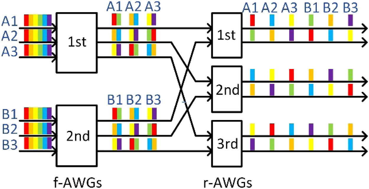
Fig. 1. Diagram of wavelength routing of a 6 × 6 WR N = 2 M = 3
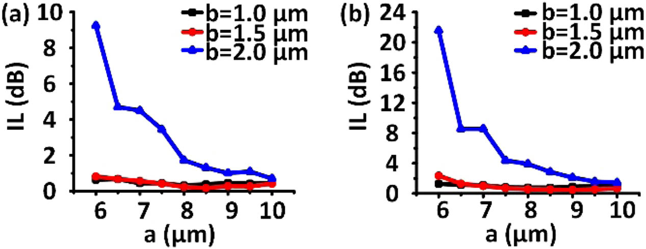
Fig. 2. Simulated ILs of (a) 2 × 2 3 × 3 a b
Fig. 3. (a)–(c) Diagrams of three connecting cases when the fan-out angle (θ L x L y S θ
Fig. 4. (a) Optimized interconnection network of the 12 × 12 WR
Fig. 5. Microscope image of the fabricated 12 × 12
Fig. 6. (a) Measured ILs of 3 × 3 4 × 4 12 × 12
Fig. 7. Measured bit error rate (BER) curves at 10 Gb/s and eye diagram when received optical power is − 20 dBm

Set citation alerts for the article
Please enter your email address
© Copyright 2018-2021 | Chinese Laser Press. All Rights Reserved 沪ICP备15018463号-20