Abstract
With the rapidly increasing bandwidth requirements of optical communication networks, compact and low-cost large-scale optical switches become necessary. Silicon photonics is a promising technology due to its small footprint, cost competitiveness, and high bandwidth density. In this paper, we demonstrate a silicon wavelength routing switch employing cascaded arrayed waveguide gratings (AWGs) connected by a silicon waveguide interconnection network on a single chip. We optimize the connecting strategy of the crossing structure to reduce the switch’s footprint. We develop an algorithm based on minimum standard deviation to minimize the port-to-port insertion loss (IL) fluctuation of the switch globally. The simulated port-to-port IL fluctuation decreases by about 3 dB compared with that of the conventional one. The average measured port-to-port IL is 13.03 dB, with a standard deviation of 0.78 dB and a fluctuation of 2.39 dB. The device can be used for wide applications in core networks and data centers.1. INTRODUCTION
The emergence of new bandwidth-hungry internet applications, such as cloud computing, super-high-definition video, and virtual reality, has driven dramatic internet traffic growth in recent years. In backbone and metro networks, reconfigurable optical add/drop multiplexers become key elements because they route optical signals directly in the optical domain [1]. When the number of wavelengths transmitted and nodes are large, compact and low-cost optical switches are urgently required. Furthermore, data centers providing bulk data interaction are expected to reduce switching cost and power consumption [2]. For this purpose, large-scale optical switches with modular growth capabilities should be developed.
At present, there are many different types of optical switching technologies, such as micro-electromechanical system switches [3,4], semiconductor-optical-amplifier-based switches [5,6], wavelength-selective switches [7], and wavelength routing (WR) switches [8,9]. Switching scalability and switching speed become two essential parameters to determine approach effectiveness [10]. The wavelength routing approach, which combines wavelength tunable lasers and arrayed waveguide grating routers (AWGRs), exhibits some unique advantages. The switching time can be less than 100 ns, and the switch port count is able to exceed . Modular growth capability and lower total crosstalk level are also strengths of WR switches. A WR switch based on a planar lightwave circuit platform was developed using ninety DC switches and three arrayed waveguide grating (AWG) subsystems [8]. However, the volume of such a WR switch is still too large, and hundreds of fibers have to be used to connect different subsystems.
Silicon photonics has made notable advances over the last decade [11,12]. Silicon-on-insulator (SOI) is an attractive platform with a compact footprint to resolve the above-mentioned problems. Notice that an optical interconnection can be a main barrier against realizing this. All cross connections have to be done in a single layer. Therefore, low-loss and low-crosstalk crossings are essential. Several approaches have been proposed to reduce the crossing loss and crosstalk in recent years [13–16]. Meanwhile, the complexity of the interconnection network may rapidly increase with the port number. Typically, some short waveguides could be routed freely with no crossings, but some long waveguides may encounter a dozen of crossings [17], leading to a serious fluctuation of insertion loss (IL) among all port-to-port paths and a degradation of transmission performance. Such an unbalanced IL feature may get worse, along with the increasing port scale of WR switches.
Sign up for Photonics Research TOC. Get the latest issue of Photonics Research delivered right to you!Sign up now
In this work, we design and experimentally demonstrate an on-chip silicon WR switch based on cascaded cyclic AWGs connected by an optimally designed silicon waveguide interconnection network. To reduce the footprint of each crossing structure, we propose a connecting strategy between each cross node and straight waveguide. By considering the IL profiles of the AWGs and the interconnection network, we develop an optimization algorithm based on minimum standard deviation to minimize the port-to-port IL fluctuation of the switch globally. With an ultracompact device footprint of , the simulated IL fluctuation can be significantly decreased to 0.37 dB, and the measured one of the fabricated device is only 2.39 dB, which implies that the proposed on-chip switch can be an excellent candidate of compact optical switches for optical communication networks and data centers.
2. DESIGN
Theoretically, a WR switch consists of two groups of small AWGs with different port counts, including cyclic AWGs (front []-AWG) and AWGs (rear []-AWG) [8]. It is capable of routing an input optical signal to any output port by tuning to a selected wavelength at any input port. Figure 1 shows an example of the wavelength routing characteristics of the WR switch when and . The proposed WR switch is designed on the SOI platform with a 220 nm top silicon layer on top of a 2 μm oxide layer. The switch consists of three cyclic AWGs (-AWG) and four cyclic AWGs (-AWG). The channel spacing of both types of AWGs is 400 GHz. The free spectral ranges (FSRs) of f-AWG and r-AWG are 1600 and 1200 GHz, respectively. Then, the effective FSR of the switch is 4800 GHz. The -AWGs and -AWGs are connected with a silicon waveguide interconnection network. The designed central frequencies of the total 12 wavelength channels of the switch are from 191.05 THz to 195.45 THz.
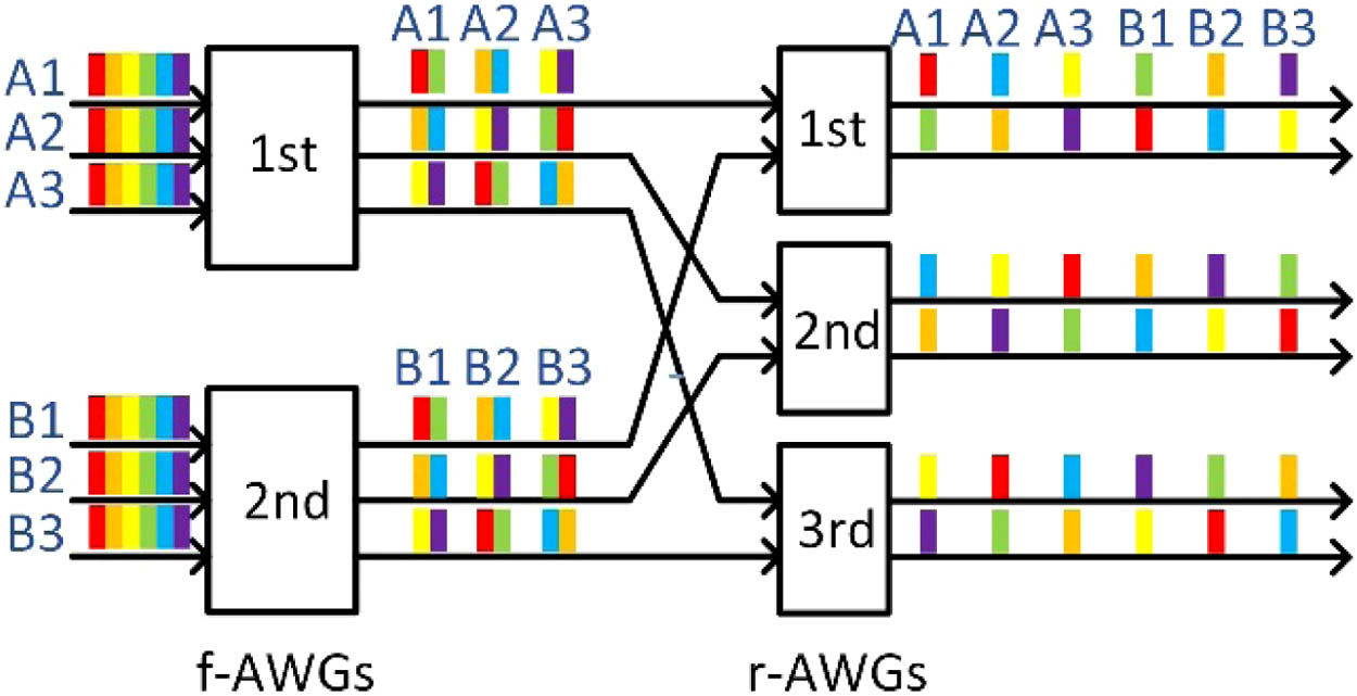
Figure 1.Diagram of wavelength routing of a switch ( and ). Six kinds of small blocks with different colors represent different wavelengths.
In the interconnection network, there would be a large number of waveguide crossings. Simple crossings may exhibit high loss due to excitation of radiation modes and high crosstalk by coupling to the guided modes of the intersecting waveguide [18]. Here, elliptical crossings are used to reduce insertion loss and crosstalk [19]. In general, we may realize all crossings using fourfold symmetric crossings if the device footprint is large enough. However, as the scale of switch ports increases, the number of crossings will increase significantly, probably leading to an aggressively expanded footprint to maintain low crosstalk between adjacent crossings. Thus, we propose to use sixfold symmetric elliptical crossings to realize a more compact interconnection network. Using Lumerical FDTD Solutions, we designed elliptical crossings by optimizing the geometric parameters [19]. To obtain a small footprint, the length of crossings is limited to be less than 20 μm. Figure 2 shows the simulated ILs versus the length of semi-major axis (a) and semi-minor axis (b) of the elliptical region. For the optimized crossing, the IL is 0.18 dB with and of 8.5 μm and 1.5 μm, respectively. And, for the optimized crossing, the IL is 0.48 dB with a and of 9 μm and 1.5 μm, respectively.

Figure 2.Simulated ILs of (a) crossings and (b) crossings as a function of semi-major axis and semi-minor axis of the elliptical region.
In practice, bent waveguides will be employed to connect freely routed straight silicon waveguides and the crossings with fixed intersection angles. To reduce the space occupied by such bends, we propose an optimized connecting strategy based on the fan-out angle () between the straight waveguide and the major axis of the elliptical region of the crossing. In this work, we set the radius of all bends () to be 20 μm to minimize bending loss. Generally, as shown in Fig. 3(b), two bends, 1 and 2, are connected with the elliptical region, and another two bends, 3 and 4, are connected with the straight waveguides. Bends 1 and 3, as well as 2 and 4, are tangent. Then, the lengths of the two sides of the connecting area can be expressed as where and represent the lengths of horizontal and vertical sides of the connecting area, respectively, and and are the central angles of the two types of bends, respectively, which can be obtained by
Figure 3.(a)–(c) Diagrams of three connecting cases when the fan-out angle () is 0°, 45°, and 90°, respectively, and related parameters are marked. (d) Horizontal length (), longitudinal length (), and square area () of the connecting area as a function of .
Figure 3(d) shows the profiles of , , and the rectangular area versus different fan-out angles. We can find that increases at first and reaches a peak value at , while it decreases after that until and finally equals . At the same time, both and almost monotonically increase with the increase of . Thus, during the process of connecting straight waveguides and elliptical regions of crossings, we should try to decrease the fan-out angles by rotating the crossings or straight waveguides to reduce the device footprint.
As for the IL fluctuation among all port-to-port paths of the switch, it mainly comes from two aspects. One is the nonuniform IL feature of each AWG, which is defined as the difference in IL between the central channel and the outer channels [20]. The other is the difference in the number of crossings among the 12 paths of the interconnection network. For a conventional configuration of such a network, the th output port of the th f-AWG is connected with the th input port of the th -AWG, where and are the respective indices of the f-AWGs/r-AWGs, respectively [8]. In fact, to realize a nonblocking WR switch, it is required only that different output ports of each -AWG should be connected with input ports of different -AWGs, respectively. There is room to optimize the interconnection network to obtain a trade-off between the IL fluctuation and the average IL.
First, for each -AWG, four output ports are assigned to connect with four -AWGs, so the number of possible assignments of each -AWG is 4!. Then, the three input ports of each -AWG are assigned to connect with three output ports from three different -AWGs, so the number of possible assignments of each -AWG is 3!. As a result, the total number of possible connection configurations is . Here, we may theoretically analyze the IL profile of each possible configuration and select the best one as the optimized scheme. In general, we draw the logical connection matrix of each possible configuration first. Then, we replace each logical cross node of each connection with one crossing based on the connecting strategy we proposed before. If two neighboring cross nodes are too close to place two crossings, one crossing is used to bridge the related three waveguides. The simulated ILs of and crossings are 0.18 dB and 0.48 dB, as mentioned above. The simulated central ILs of the AWG and the AWG are 1.26 dB and 1.42 dB, respectively, and their IL fluctuations are 1.26 dB and 1.57 dB, respectively. Finally, we use the standard deviation to evaluate the port-to-port IL fluctuation of the switch, given by where and are the standard deviation and the mean value of the ILs of the 12 paths, respectively, and is the IL of the th path. For simplicity, the signal is injected into the central input ports of -AWGs and coupled out from the central output ports of -AWGs to evaluate the port-to-port IL performance versus the path number of the connection network. In our simulations, a minimized is preferred. The optimized logical connection configuration given in Figs. 4(a) and 4(b) shows the simulated IL profiles of the conventional and optimized configuration. It can be found clearly that the performance of IL fluctuation is greatly improved. Specifically, the IL fluctuation of the conventional configuration reaches 3.37 dB, while the optimized one is significantly decreased to 0.37 dB. At the same time, a decreased IL fluctuation comes at the expense of increased average IL. The average IL increases to 5.30 dB after optimization, which is slightly larger than 4.91 dB of the conventional one.
Figure 4.(a) Optimized interconnection network of the switch. (b) Simulated port-to-port IL profiles of the conventional and the optimized interconnection networks.
3. FABRICATION AND MEASUREMENT
We fabricated the proposed switch on an SOI wafer with a 220 nm silicon top layer and a 2 μm silica substrate. The pattern is defined using electron beam lithography with a 330 nm ZEP-520A resist layer spun on the samples. Then, the top silicon layer is etched using inductively couple plasma etching technology.
Figure 5 shows the microscope image of the fabricated silicon WR switch consisting of three cyclic AWGs, four cyclic AWGs, and one interconnection network. Two and crossings are used in the physical interconnection network with the same configuration as the logical one given in Fig. 4(a). A pair of uniform grating couplers are used to couple the light into and out of the silicon waveguides. We also fabricated stand-alone -AWGs, -AWGs, and interconnection networks, which were coupled directly with grating couplers for measuring the IL performance independently.
Figure 5.Microscope image of the fabricated silicon WR switch and zoomed-in crossing structure.
The measured IL profiles are given in Fig. 6. The measured central frequencies of the total 12 wavelength channels are from 191.54 THz to 195.78 THz. The measured average ILs of crossings and crossings are 0.29 dB and 0.84 dB, respectively. As shown in Fig. 6(a), the measured average ILs of -AWGs and -AWGs are 3.76 dB and 3.00 dB, respectively. For both types of AWGs, the ILs of the outer channels are significantly larger than that of the central channel. The IL fluctuations caused by the nonuniformity of the -AWG and the r-AWG are 1.65 dB and 1.37 dB, respectively. In Fig. 6(b), the average measured profiles of the total port-to-port IL and reference interconnection networks’ ILs are given. Furthermore, an estimated average IL profile introduced by both -AWG and -AWG is also shown by subtracting the average interconnection network IL from the average total IL. As expected, the IL profile of the interconnection network drops sharply at the two outer paths and maintains a small IL ripple at other paths. The measured total IL in average is 13.03 dB, with a standard deviation of 0.78 dB and a fluctuation of 2.39 dB. We also found that the interconnection network IL profile was robust to fabrication errors. But the central wavelength mismatch between the two channels of the -AWG and -AWG in each routing path was more likely to be affected by fabrication errors, leading to extra losses in some paths and an increasing port-to-port IL fluctuation. We also measured the bit error rate of the silicon WR switch at 10 Gb/s, as shown in Fig. 7.
Figure 6.(a) Measured ILs of AWG and AWG. (b) Measured total IL of the silicon WR switch for different transmission paths, reference interconnection network IL and AWG IL, which is given by subtracting the average reference interconnection network IL from the average total IL.
Figure 7.Measured bit error rate (BER) curves at 10 Gb/s and eye diagram when received optical power is .
4. CONCLUSION
In this paper, we demonstrated an on-chip switch based on cascaded small AWGs on an SOI platform. This WR switch consists of three cyclic AWGs and four cyclic AWGs connected by a silicon waveguide interconnection network. We proposed the connecting strategy based on the fan-out angle between the straight waveguide and the major axis of the elliptical region of the crossing to reduce the footprint. We also developed the optimized algorithm based on minimum standard deviation to minimize the port-to-port IL fluctuation of the switch derived from the nonuniformity of AWGs and the difference of the number of crossings in different paths. Compared with the conventional one, the simulated IL fluctuation decreases by 3 dB. Then, we fabricated the optimized switch on the SOI wafer. The measured total IL in average is 13.03 dB, with a standard deviation of 0.78 dB and a fluctuation of 2.39 dB. It may offer great prospects for applications on compact optical switches in optical communication networks and data centers.
References
[1] S. Gringeri, B. Basch, V. Shukla, R. Egorov, T. J. Xia. Flexible architectures for optical transport nodes and networks. IEEE Commun. Mag., 48, 40-50(2010).
[2] C. Kachris, K. Kanonakis, I. Tomkos. Optical interconnection networks in data centers: recent trends and future challenges. IEEE Commun. Mag., 51, 39-45(2013).
[3] W. M. Mellette, G. M. Schuster, G. Porter, G. Papen, J. E. Ford. A scalable, partially configurable optical switch for data center networks. J. Lightwave Technol., 35, 136-144(2017).
[4] T. Seok, N. Quack, S. Han, R. Muller, M. Wu. Large-scale broadband digital silicon photonic switches with vertical adiabatic couplers. Optica, 3, 64-70(2016).
[5] R. Stabile, A. A. Mejia, K. A. Williams. Monolithic active passive 16 × 16 optoelectronic switch. Opt. Lett., 37, 4666-4668(2012).
[6] Q. Cheng, A. Wonfor, J. L. Wei, R. V. Penty, I. H. White. Low-energy, high-performance lossless 8 × 8 SOA switch. Optical Fiber Communication Conference and Exhibition (OFC), 1-3(2015).
[7] N. Farrington, A. Forencich, P. C. Sun, S. Fainman, J. Ford, A. Vahdat, G. Porter, G. C. Papen. A 10 μs hybrid optical-circuit/electrical-packet network for datacenters. Optical Fiber Communication Conference/National Fiber Optic Engineers Conference, OW3H.3(2013).
[8] K. Sato, H. Hasegawa, T. Niwa, T. Watanabe. A large-scale wavelength routing optical switch for data center networks. IEEE Commun. Mag., 51, 46-52(2013).
[9] K. Ueda, Y. Mori, H. Hasegawa, K. I. Sato, T. Watanabe. Large-scale optical-switch prototypes utilizing cyclic arrayed-waveguide gratings for datacenters. J. Lightwave Technol., 34, 608-617(2016).
[10] A. Vahdat. Delivering scale out data center networking with optics—why and how. Optical Fiber Communication Conference and Exposition and the National Fiber Optic Engineers Conference (OFC/NFOEC), 1-36(2012).
[11] A. Rickman. The commercialization of silicon photonics. Nat. Photonics, 8, 579-582(2014).
[12] M. J. R. Heck, J. F. Bauters, M. L. Davenport, J. K. Doylend, S. Jain, G. Kurczveil, S. Srinivasan, Y. Tang, J. E. Bowers. Hybrid silicon photonic integrated circuit technology. IEEE J. Sel. Top. Quantum Electron., 19, 6100117(2013).
[13] Y. Zhang, A. Hosseini, X. Xu, D. Kwong, R. T. Chen. Ultralow-loss silicon waveguide crossing using Bloch modes in index-engineered cascaded multimode-interference couplers. Opt. Lett., 38, 3608-3611(2013).
[14] P. J. Bock, P. Cheben, J. H. Schmid, J. Lapointe, A. Delâge, D. X. Xu, S. Janz, A. Densmore, T. J. Hall. Subwavelength grating crossings for silicon wire waveguides. Opt. Express, 18, 16146-16155(2010).
[15] Y. Ma, Y. Zhang, S. Yang, A. Novack, R. Ding, A. E. J. Lim, G. Q. Lo, T. B. Jones, M. Hochberg. Ultralow loss single layer submicron silicon waveguide crossing for SOI optical interconnect. Opt. Express, 21, 29374-29382(2013).
[16] P. Sanchis, J. V. Galán, A. Griol, J. Martí, M. A. Piqueras, J. M. Perdigues. Low-crosstalk in silicon-on-insulator waveguide crossings with optimized-angle. IEEE Photon. Technol. Lett., 19, 1583-1585(2007).
[17] M. P. Earnshaw, J. B. D. Soole, M. Cappuzzo, L. Gomez, E. Laskowski, A. Paunescu. 8 × 8 optical switch matrix using generalized Mach–Zehnder interferometers. IEEE Photon. Technol. Lett., 15, 810-812(2003).
[18] H. Subbaraman, X. Xu, A. Hosseini, X. Zhang, Y. Zhang, D. Kwong, R. T. Chen. Recent advances in silicon-based passive and active optical interconnects. Opt. Express, 23, 2487-2511(2015).
[19] T. Fukazawa, T. Hirano, F. Ohno, T. Baba. Low loss intersection of Si photonic wire waveguides. Jpn. J. Appl. Phys., 43, 646-647(2004).
[20] X. J. M. Leijtens, H. Venghaus, B. Kuhlow, M. K. Smit. Arrayed waveguide gratings. Wavelength Filters in Fiber Optics, 125-187(2006).


