• Chinese Optics Letters
  • Vol. 22, Issue 2, 022501 (2024)
Qiushuang Chen1、2, Li Chen1、2、*, Cong Chen1、2, Ge Gao1, Wei Guo1、2, and Jichun Ye1、2、**
Author Affiliations
  • 1Ningbo Institute of Materials Technology and Engineering, Ningbo 315201, China
  • 2University of Chinese Academy of Sciences, Beijing 100049, China
  • show less
    DOI: 10.3788/COL202422.022501 Cite this Article Set citation alerts
    Qiushuang Chen, Li Chen, Cong Chen, Ge Gao, Wei Guo, Jichun Ye. Carrier transport barrier in AlGaN-based deep ultraviolet LEDs on offcut sapphire substrates[J]. Chinese Optics Letters, 2024, 22(2): 022501 Copy Citation Text show less
    AFM images and corresponding line profile of the MQWs grown on (a) the 0.2° offcut substrate and (b) the 1° offcut substrate. (c) The FWHM of XRCs and (d) the Raman spectra of the MQWs grown on the 0.2° and 1° offcut substrates.
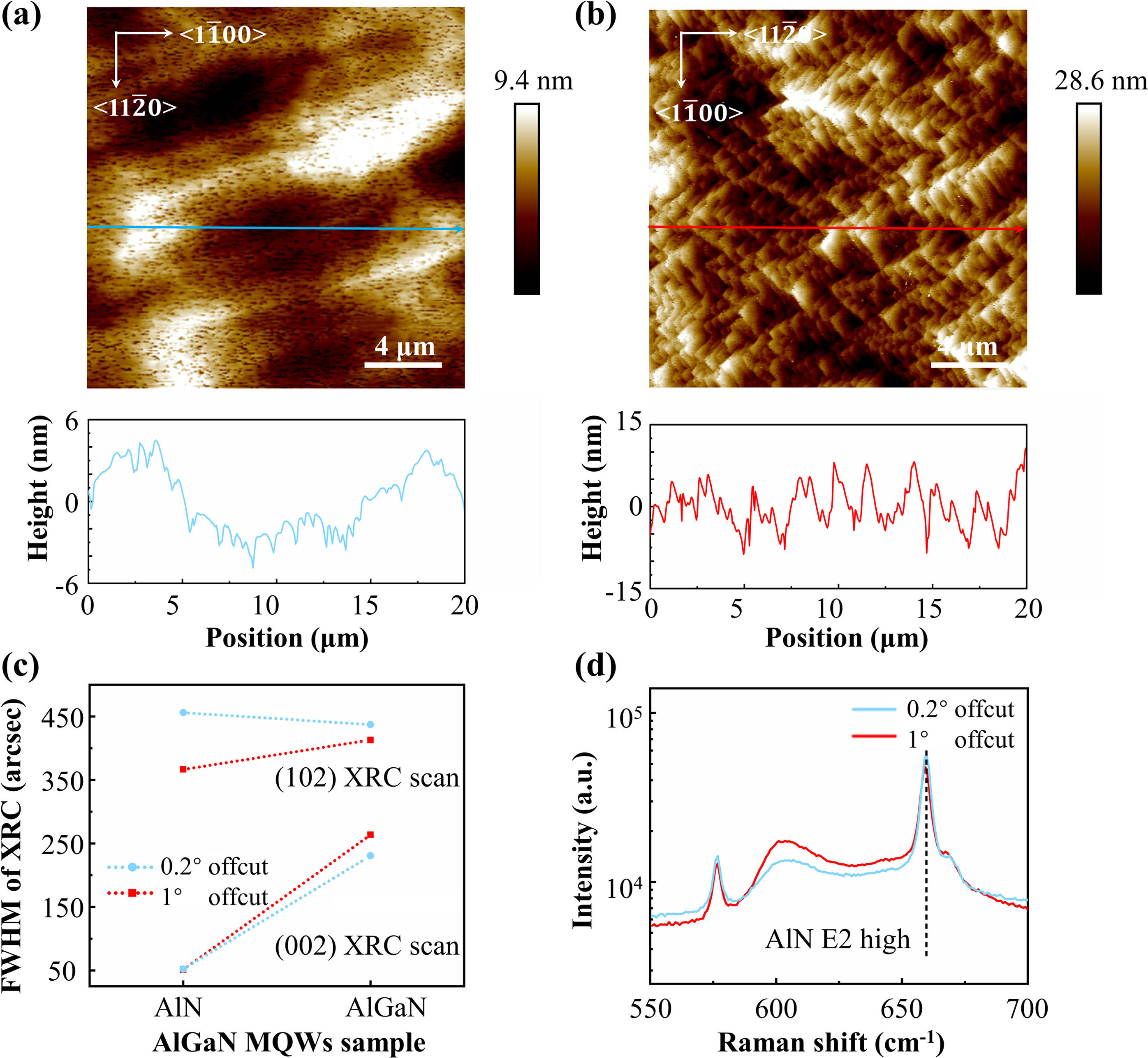
    Fig. 1. AFM images and corresponding line profile of the MQWs grown on (a) the 0.2° offcut substrate and (b) the 1° offcut substrate. (c) The FWHM of XRCs and (d) the Raman spectra of the MQWs grown on the 0.2° and 1° offcut substrates.
    EL spectra under the different injection current of (a) the 0.2° and (b) 1° offcut DUV LEDs. (c) The EL spectra at the 20 mA injection condition. (d) I-V curves of the two LEDs. (e) The integral EL intensity as a function of the different injection currents.
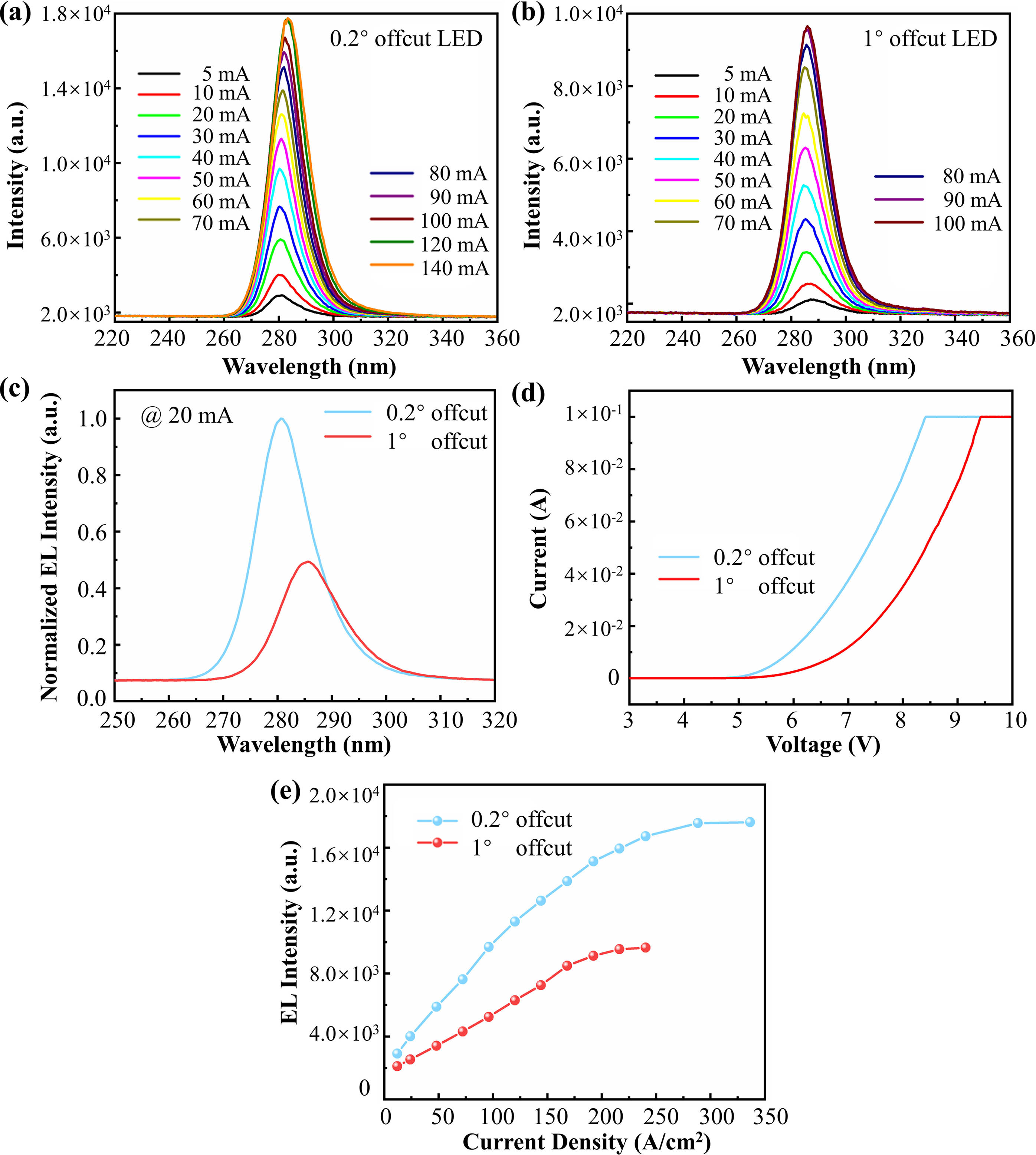
    Fig. 2. EL spectra under the different injection current of (a) the 0.2° and (b) 1° offcut DUV LEDs. (c) The EL spectra at the 20 mA injection condition. (d) I-V curves of the two LEDs. (e) The integral EL intensity as a function of the different injection currents.
    (a) PL spectra of the MQWs grown on the 0.2° and 1° offcut substrates. (b) The integrated PL intensity and (c) emission wavelength mapping of the hexagonal pyramid. The inset OM image shows the hexagonal column and pyramid on the 0.2° offcut sapphire substrate. (d) The IQE values of the two MQWs samples with different laser excitation power.
    Fig. 3. (a) PL spectra of the MQWs grown on the 0.2° and 1° offcut substrates. (b) The integrated PL intensity and (c) emission wavelength mapping of the hexagonal pyramid. The inset OM image shows the hexagonal column and pyramid on the 0.2° offcut sapphire substrate. (d) The IQE values of the two MQWs samples with different laser excitation power.
    (a) SEM image, (b) panchromatic CL intensity mapping, and (c) CL spectra across the steps of the MQWs grown on the 0.2° offcut substrate. (d) SEM image, (e) panchromatic CL intensity mapping, and (f) CL spectra across the steps of MQWs grown on the 1° offcut substrate.
    Fig. 4. (a) SEM image, (b) panchromatic CL intensity mapping, and (c) CL spectra across the steps of the MQWs grown on the 0.2° offcut substrate. (d) SEM image, (e) panchromatic CL intensity mapping, and (f) CL spectra across the steps of MQWs grown on the 1° offcut substrate.
    (a) Schematic diagram of the current direction and step topography. (b) The I-V characters between the n-electrodes in the linear coordinate with error bars and (c) between the n- and p-electrode in the semi-log axis with error bars for both the 0.2° and 1° offcut samples in the two directions.
    Fig. 5. (a) Schematic diagram of the current direction and step topography. (b) The I-V characters between the n-electrodes in the linear coordinate with error bars and (c) between the n- and p-electrode in the semi-log axis with error bars for both the 0.2° and 1° offcut samples in the two directions.
    (a), (b) Cross-sectional HAADF images and (c), (d) corresponding composition distribution of the Al and Ga elements along the yellow arrow in the HAADF images by the EDS of the AlGaN-based LED grown on the 0.2° and 1° offcut sapphire, respectively.
    Fig. 6. (a), (b) Cross-sectional HAADF images and (c), (d) corresponding composition distribution of the Al and Ga elements along the yellow arrow in the HAADF images by the EDS of the AlGaN-based LED grown on the 0.2° and 1° offcut sapphire, respectively.
    2θ-ω scans of the n-AlGaN layer along the AlN (0002) diffraction.
    Fig. 7. 2θ-ω scans of the n-AlGaN layer along the AlN (0002) diffraction.
    (a), (b) Numerical simulation structure and (c), (d) relevant conduction band mapping of AlGaN-based LED grown on 0.2° and 1° offcut sapphire. (e) Band structure along the cutline. (f) Three-dimensional schematic about actual carrier spreading under the influence of potential assisted with step structures.
    Fig. 8. (a), (b) Numerical simulation structure and (c), (d) relevant conduction band mapping of AlGaN-based LED grown on 0.2° and 1° offcut sapphire. (e) Band structure along the cutline. (f) Three-dimensional schematic about actual carrier spreading under the influence of potential assisted with step structures.
    (a), (b) I-V characteristics between the n-type and the p-type electrodes in the semi-logarithmic axis under repeated tests for both the 0.2° and 1° offcut samples in two directions, respectively.
    Fig. 9. (a), (b) I-V characteristics between the n-type and the p-type electrodes in the semi-logarithmic axis under repeated tests for both the 0.2° and 1° offcut samples in two directions, respectively.
    Qiushuang Chen, Li Chen, Cong Chen, Ge Gao, Wei Guo, Jichun Ye. Carrier transport barrier in AlGaN-based deep ultraviolet LEDs on offcut sapphire substrates[J]. Chinese Optics Letters, 2024, 22(2): 022501
    Download Citation