
Qiushuang Chen, Li Chen, Cong Chen, Ge Gao, Wei Guo, Jichun Ye. Carrier transport barrier in AlGaN-based deep ultraviolet LEDs on offcut sapphire substrates[J]. Chinese Optics Letters, 2024, 22(2): 022501
- Chinese Optics Letters
- Vol. 22, Issue 2, 022501 (2024)
Abstract
1. Introduction
In recent years, public health and safety have been in the spotlight due to recurrent epidemics of Corona Virus Disease 2019 (COVID-19). Under such circumstances, the application of deep ultraviolet (DUV) light sources is booming, especially the DUV solid-state light-emitting diodes (LEDs). Compared to traditional DUV sources, AlGaN-based solid-state emitters are promising in various fields due to their advantages of being mercury-free, environmentally friendly, compact, and having low power consumption[1–4]. For instance, the utilization of micro-LED technology, characterized by reduced dimensions and enhanced brightness and contrast ratios, has brought about improved pixel density and more vivid display capabilities[5]. The integration of DUV-LEDs with -based microcavities enables high-speed ultraviolet light communication[6]. Despite so many efforts in application, AlGaN-based DUV-LEDs still face many challenges[4]. Most of the reported external quantum efficiencies (EQEs) of DUV LEDs are still below 10%[7–9], which are much lower than commercial blue LEDs based on InGaN multiple quantum wells (MQWs)[10,11]. One of the critical challenges is the crystal quality of AlGaN epilayers, which are the building blocks of the high-efficiency AlGaN-based DUV LEDs. In fact, due to the intrinsic lattice mismatch and thermal mismatch between AlGaN and sapphire[12], high-density threading dislocations arise and propagate in the epitaxial film, acting as non-radiative recombination centers and reducing the emission efficiency[13,14].
Despite the poor crystal quality of AlGaN and InGaN epitaxial layers, the inhomogeneous In content in InGaN MQWs localizes more carriers and forms the radiative recombination centers (RRCs) that can efficiently enhance the photonic emission[15–18]. In contrast, such RRCs are not found in AlGaN MQWs with fully miscible Al and Ga atoms. Recently, many scientists have tried to develop artificial localization structures to improve the internal quantum efficiency (IQE) and EQE of AlGaN-based LEDs[19–23]. The AlGaN MQWs grown on offcut substrates are often reported to have better crystal quality and IQE than planar structures[21,24,25]. Most reports suggest that Ga accumulation at the step edges on offcut sapphire can enhance the carrier localization effects, leading to bright luminescence at the step edge[19,22,24]. Several theoretical models have also been proposed to explain the relationship between luminescence and carrier transport of step-bunching MQWs[26–29]. Kojima et al. reported a carrier localization model to clarify the relationship between the luminescence and current path in uneven quantum wells[26,27]. Nagasawa et al. illustrated the relationship of dense macro-steps and inhomogeneous optical properties using a two-dimensional cathodoluminescence (CL) analysis[28]. Their group further elaborated on the Ga-rich current path assisting carrier localization by dense macro-steps on the sample of 1° offcut miscut sapphire[29]. Nevertheless, the above conclusions are based on photoluminescence (PL) and CL measurements, and the carrier transport mechanism of DUV LEDs on the offcut sapphire substrate is still under debate. Nagasawa et al. reported that the utilization of misorientation substrates induces modulation of both the composition and well thickness, leading to discrete EL emissions[30]. Xu et al. proposed that the crystal quality is not directly related to the localized current. The higher carrier concentration at the step edge under electrical injection is caused by a stronger localization effect caused by the Ga-rich region[31]. However, there is no detailed information about the influence of carrier transport barriers under electrical pumping on the performance of LEDs grown on different offcut angles.
In this work, we focus on the carrier transport process in DUV LEDs on offcut and planar sapphire substrates. Carrier transport and confinement were comprehensively studied in MQWs on offcut and planar sapphire by both optical and electrical pumping. Theoretical calculations were performed based on TEM-measured structures and further explained the relationship between the enriching Ga steps and carrier transport. A carrier transport barrier was introduced to clarify the behavior of different offcut samples.
Sign up for Chinese Optics Letters TOC. Get the latest issue of Chinese Optics Letters delivered right to you!Sign up now
2. Experiments
The DUV LEDs were grown by an Aixtron MOCVD (metal organic chemical vapor deposition) equipped with a close-coupled showerhead using different offcut sapphire substrates. Hydrogen () and nitrogen () were used as carrier gases and trimethylaluminum (TMAl), trimethylgallium (TMGa), and ammonia () as precursors for Al, Ga, and N, respectively. First, a thin layer of low-temperature AlN was deposited on the substrate as a nucleation layer, and a 2-µm-thick high-temperature AlN was grown as the template. Ten pairs of AlN/AlGaN superlattices were then introduced to filter dislocations effectively, and a 3-µm-thick Si-doped was used for the -type. After that, four periods of AlGaN MQWs were grown, including 4-nm-thick quantum wells and 10-nm-thick quantum barriers. The electron blocking layer, the contact layer, and the capping layer were subsequently deposited on top. In addition, the MQWs samples were grown directly on the AlN templates to investigate the surface and optical behaviors, and only was grown on the AlN layer to study the influence of step structures on electrical performance and composition fluctuations. The growth parameters for the MQWs are the same for all samples to better compare the discrepancy/inconsistency of AlGaN-based LEDs on different offcut sapphires. In addition, -type and -type electrodes were deposited, respectively, to investigate the electrical performance. The mesa mask was deposited on the film surface by photolithography, and the isolation was defined by an inductively coupled plasma with reactive ion etching with a target depth of 500 nm. The metal contacts were deposited using a ZZS 500 e-beam, and the pattern was constructed using lift-off technology, followed by a rapid thermal annealing in an RTP-500 rapid thermal processor. The Ti/Al/Ni/Au electrodes with 20 nm/120 nm/20 nm/50 nm in thickness were deposited on the followed by an RTA at 1000°C for 60 seconds in a ambient. Subsequently, 30 nm/50 nm thick Ni/Au was prepared and used as the -type electrodes to form the ohmic contact. Each electrode unit consists of four rectangular -type electrodes and a large surrounding -type electrode with a distance of 50 µm between each unit.
The surface morphology was measured by Bruker Dimension ICON scanning probe microscopy with a tapping mode. High-resolution X-ray diffraction with Cu source (Bruker D8 Discover) was used to study the crystalline quality. The residual stain was characterized by Raman spectrum using a 532-nm laser (Renishaw inVia Reflex). Macroscale (millimeter scale) photoluminescence of the MQWs was performed using a Coherent Ar-F excimer laser with a helium cryostat at a 193 nm target, and the emitted light was collected by a Horiba iHR550 spectrometer. A 266-nm laser was also used as a pump source, configured on a Renishaw Raman system, to study the photoluminescence at the microscale on the specific region. Cathodoluminescence was performed using the Horiba MP 325 CL system. Electroluminescence of the chip was collected by the Choptics IS30-6T integrating sphere and processed and analyzed by a Zolix 300i spectrometer. The current-voltage (I-V) curves of the LEDs were characterized by a Keithley 4200-SCS semiconductor system equipped with a shock absorber and metal shield. The sheet resistance of the films was measured by an HP-5500C Hall effect testing instrument. Cross-section slice samples were prepared by the Helios-G4-CX dual-beam-focused ion beam and further characterized by the Talos F200x transmission electron microscope.
3. Results and Discussion
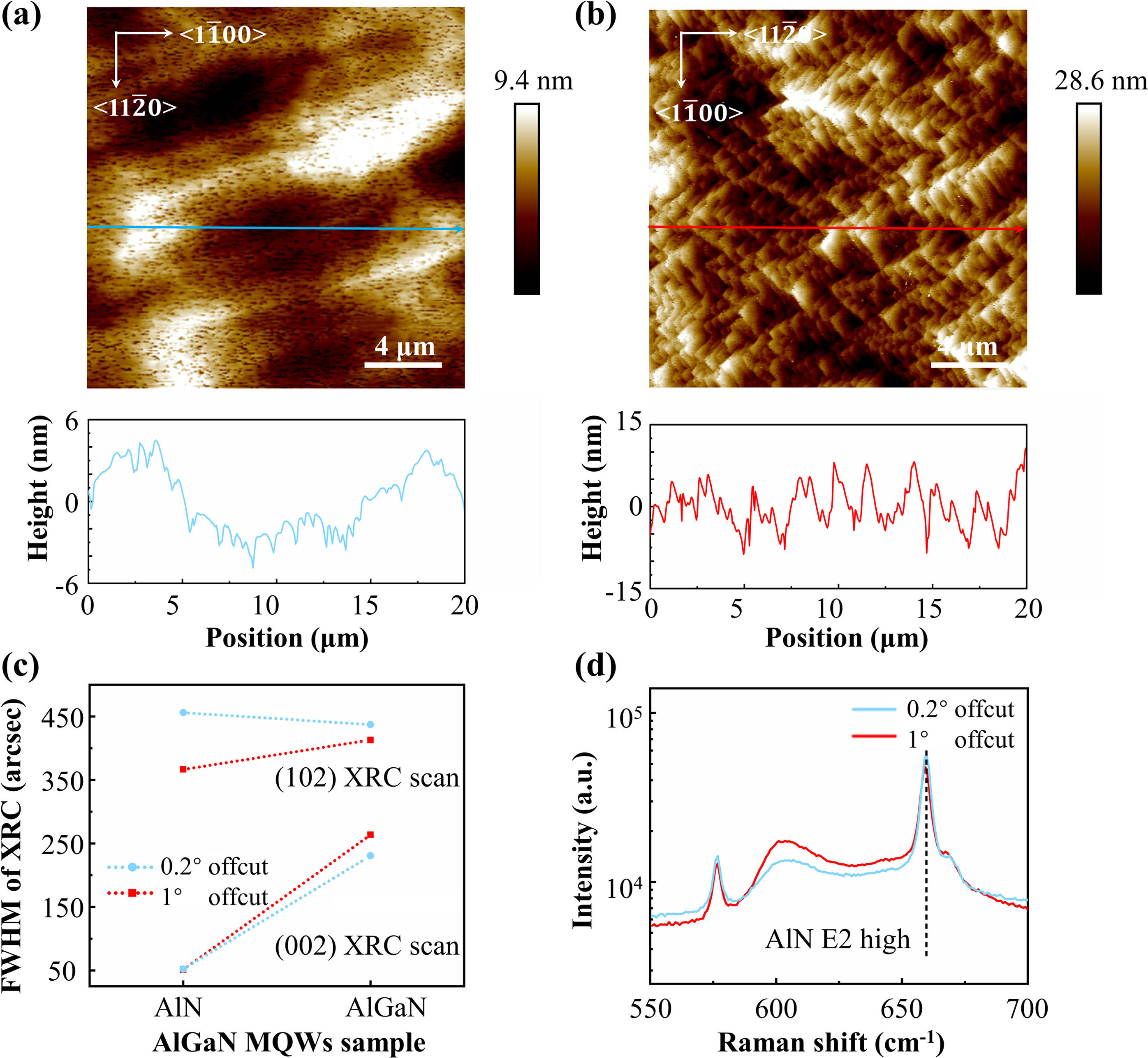
AFM images of the AlGaN MQWs on the 0.2° and 1° offcut sapphire substrates are shown in Figs. 1(a) and 1(b), respectively. Two samples exhibit step morphology with different step shapes and densities. Figure 1(a) shows the surface morphology and corresponding line profile of the MQWs on the 0.2° offcut sapphire. The presence of stripe-shaped microsteps of about 4-nm- high and 15-µm-wide indicates a low step density in the MQWs. However, the MQWs on the 1° offcut sapphire in Fig. 1(b) shows high density stacked V-shaped steps. According to the height profile, steps with an average height of 5 nm and a width of 1 µm were observed. The surface morphology of the AlGaN MQWs is strongly influenced by the offcut angles of the sapphire substrates. The distinct step bunching characteristics are attributed to the anisotropic growth rates of the -plane and -plane in the nitride materials[26,32,33]. As shown in Fig. 1(c), the full-width at half-maximum (FWHM) values of the X-ray diffraction rocking curve (XRC) of the AlGaN MQWs (0002) plane are 232 and 265 arcsec for the 0.2° and 1° offcut samples and 439 and 412 arcsec for the XRC of the AlGaN MQWs on the 0.2° and 1° offcut substrate, respectively. Correspondingly, the screw-type and edge-type threading dislocation densities can be calculated from the FWHM[34], which are and for the 0.2° sample and and for the 1° sample, showing a similar crystalline quality on the different offcut substrates. The strain states of the two samples were also compared by Raman spectra in Fig. 1(d). The E2 (high) of the AlN for both samples are located at , showing compressive strain compared to the unstrained AlN at [35].
![]()
Figure 1.AFM images and corresponding line profile of the MQWs grown on (a) the 0.2° offcut substrate and (b) the 1° offcut substrate. (c) The FWHM of XRCs and (d) the Raman spectra of the MQWs grown on the 0.2° and 1° offcut substrates.
Based on previous reports, the structure and composition fluctuation of the MQWs on the higher offcut substrates show a stronger carrier localization effect and enhanced luminescence[24,36]. For electrically driving LED devices, EL spectra are the most useful measurement. The EL of the 0.2° and 1° offcut DUV LEDs under different driving currents were used. From Figs. 2(a) and 2(b), both exhibit the single peak emission, which is different from previous reports that a higher offcut angle leads to two separate emission peaks[23,30,37]. The single peak emission is probably related to the enhanced localization effect by the stepped topography, which is similar to the phenomenon in PL explained in the previous report[31]. Compared to the 0.2° offcut LEDs, the red shift and slight broadening are observed in the 1° offcut LEDs. For example, at an injection current of 20 mA in Fig. 2(c), the EL emission peaks of the 0.2° and 1° offcut LEDs are located at 280.67 nm and 285.73 nm with corresponding FWHM values of 13.11 and 14.33 nm, presenting a red shift of approximately 5 nm and a broadening of 1 nm for 1° offcut LEDs. Such red-shifts and spectral broadening are mainly due to the non-uniform composition distribution in step-bunched MQWs[30]. In addition, the turn-on voltage of the 1° offcut sample is higher than that of the 0.2° offcut sample, as shown in Fig. 2(d). The EL emission intensity at different injection currents from 12.0 to was also investigated. As shown in Fig. 2(e), the EL intensity of the 0.2° offcut sample is larger than that of the 1° offcut sample in the whole range. As the injection current increases from 12.0 to , the EL intensity of the 1° offcut LED reaches saturation. Unfortunately, when the injected current exceeds , the 1° offcut LED burns out due to overheating, while the luminescence intensity of the 0.2° offcut sample still increases until it saturates at . A much lower light output power and EQE of the LEDs were obtained on the higher offcut substrate, which is contrary to the reported results[26,37]. The low optical power and high driving voltage can be induced by both optical and electrical properties of the offcut samples, where the influence of step bunching structures should be considered.
![]()
Figure 2.EL spectra under the different injection current of (a) the 0.2° and (b) 1° offcut DUV LEDs. (c) The EL spectra at the 20 mA injection condition. (d) I-V curves of the two LEDs. (e) The integral EL intensity as a function of the different injection currents.
The optical and electrical factors that influence the light output power of the LED are studied separately. The optical behavior of the MQWs on the different offcut substrates has been studied in detail by PL and is shown in Fig. 3(a). A single emission peak is observed from the 1° offcut sample, which is consistent with the EL spectra above. Surprisingly, two distinct peaks appear in the 0.2° offcut sample, which are not found by EL. To illustrate the origin of the abnormal PL behavior in 0.2° MQWs, micro-scaled analysis was used. Several hexagonal columns and pyramids with diameters of about 20 µm are found on the surface of the 0.2° offcut sample by optical microscopy, two of which are shown in the inset of Fig. 3(b). Spatially resolved PL mapping is performed using confocal microscopy, and the intensity and wavelength mapping is presented in Figs. 3(b) and 3(c). It can be clearly seen that only the hexagonal pyramid exhibits peculiar luminescence separate from the main emission for the 0.2° offcut sample. The stronger localized emission with a shorter wavelength corresponds to the emission from the hexagonal pyramid, while the weaker and longer wavelength emission corresponds to the planar MQWs of the 0.2° offcut sample. The emission from the hexagonal pyramid shows a blue shift of 10 nm with respect to the planar region of the 0.2° offcut MQWs, which is consistent with the splitting of the two peaks in Fig. 3(a). However, due to the low density of the hexagonal pyramid, the integral intensity of the two emission peaks differs by less than a factor of two, even though the localized emission intensity is almost ten times higher than in the planar region. It is also noteworthy that a 5-nm red shift of the PL mapping is observed compared to the macroscale PL spectra, which is attributed to the distinction of the test condition. The macroscale PL uses a 193-nm laser with a higher photon energy, resulting in a higher photon-generated carrier energy and thus a stronger bandgap filling effect[38]. Thus, the PL peak of MQWs is blue shifted relative to the PL mapping by a 266-nm laser. In addition, both the step and terrace region are uniformly excited during optical excitation, which differs from the electrical pumping in that the carriers are more inclined to pass through the Ga-rich region with a lower barrier and a smaller bandgap[39]. Therefore, the peak of the PL emission with the two offcut LEDs is blue shifted compared to the EL excitation.
![]()
Figure 3.(a) PL spectra of the MQWs grown on the 0.2° and 1° offcut substrates. (b) The integrated PL intensity and (c) emission wavelength mapping of the hexagonal pyramid. The inset OM image shows the hexagonal column and pyramid on the 0.2° offcut sapphire substrate. (d) The IQE values of the two MQWs samples with different laser excitation power.
It is worth noting that in the PL test, the peak position of the 1° offcut sample is blue shifted with respect to the planar region on the 0.2° offcut substrate, whereas in the electric pumping, an opposite red shift is observed. This is due to the fact that the stepped topography on the offcut sapphire leads to the inhomogeneity of AlGaN composition, forming a Ga-rich localized center with lower bandgap energy, resulting in a red shift of the emission wavelength. Meanwhile, the high offcut substrate introduces high density stacked steps, leading to an increase in the number of Ga-rich localized centers and thus high Al content in the terrace, leading to an increase in the photon energy. This structure shows little effect in the EL with a selective current spreading path but becomes more serious in the PL with high power excitation in the macro-scale, which facilitates the blue shift of the 1° offcut in the MQWs in the PL condition.
Despite the anomalous two emission peaks, the radiative recombination efficiency was further investigated under different excitation powers and is shown in Fig. 3(d). It can be evaluated through the characterization of the IQE. In order to obtain the values for the IQE, PL testing is conducted at both low temperature (LT) at 10 K and room temperature (RT) at 300 K. The value of IQE can be calculated by taking the ratio of the integrated intensity of the PL emission from the RT to the LT on the MQWs sample[19]. It is assumed that the IQE value at 10 K is 100% since defect-related non-radiative recombination centers are inactive at the LT condition[22]. The MQWs of the 1° offcut sample exhibit an IQE of up to 83.1%, which is almost double that of the 0.2° offcut sample of 43.2%. The significantly improved IQE of the MQWs on the 1° offcut sapphire may benefit from the dense V-shaped steps, which were confirmed to have a strong localization effect on carriers by the CL measurement, as shown in Fig. 4. In addition, the SEM image of the MQWs grown on the 1° offcut substrate in Fig. 4(d) does not exhibit similar hexagonal columns and pyramids, as observed in the 0.2° sample. Only densely stacked V-shaped steps are observed. This further confirms that the PL peak separation from the 0.2° offcut MQWs originates from different surface conditions. The higher offcut MQWs are expected to have a better optical property, which is in good agreement with the previous reports[22,24].
![]()
Figure 4.(a) SEM image, (b) panchromatic CL intensity mapping, and (c) CL spectra across the steps of the MQWs grown on the 0.2° offcut substrate. (d) SEM image, (e) panchromatic CL intensity mapping, and (f) CL spectra across the steps of MQWs grown on the 1° offcut substrate.
The superior optical performance of the MQWs on the 1° offcut sapphire cannot explain the lower optical output power in Fig. 2. Unlike the localized photon-generated electron-hole pairs, the long-range carriers propagating under electrical injection are severely affected by the steps, as the electron is more susceptible to the carrier transport barrier. Therefore, the current path in different offcut samples should be considered. As shown in Fig. 5(a), the electrodes were prepared parallel and perpendicular to the step morphology of the AlGaN-based LEDs on the 0.2° and 1° offcut sapphire, respectively. The I-V measurements of the between two adjacent devices and the in the same device are schematically plotted in Figs. 5(b) and 5(c). The I-V curves of the along different directions and samples are shown with error bars in Fig. 5(b) from which the same order of the linear I-V curve was observed with little difference. A slightly higher slope of the 1° offcut sample is shown, especially in the perpendicular direction. As the electrical transport between the -pads is dominant in the lateral direction, which can be considered as a simple resistance model, the 1° offcut sample has a lower resistance than the 0.2° offcut sample. This result consists of the sheet resistance by Hall from which the resistance of on the 1° offcut sample is 18,000 Ω/□ and 18,800 Ω/□ for the 0.2° offcut sample. The high resistances of the two samples respond to the low current. It is noteworthy that the aforementioned two samples exhibit different electrical trends in two current directions. For the LED on the 0.2° offcut sapphire, a smaller current perpendicular to the step direction was observed, which may be related to the step structures[23]. The transport of the carriers tunneling the steps is hindered by high-resistance assisted with the steps, resulting in a lower current. The sparse density of the steps ensures that the current of the 0.2° offcut LED in the direction parallel to the steps is not affected by the resistance fluctuation. However, the opposite is the case with the 1° offcut sample, which is assisted by the shape of its steps. In the V-shaped step unit, the carriers that travel in the direction perpendicular to the steps will only tunnel a high-resistance region located at the tip of the V-shaped step. On the other hand, for the carriers traveling parallel to the step direction, they will pass through high-resistance regions located on both sides of the V-shaped step, resulting in a smaller current parallel to the step directions. However, due to the dense distribution of the V-shaped steps, the overall current difference between the two directions is not significant for the 1° offcut sample.
![]()
Figure 5.(a) Schematic diagram of the current direction and step topography. (b) The I-V characters between the n-electrodes in the linear coordinate with error bars and (c) between the n- and p-electrode in the semi-log axis with error bars for both the 0.2° and 1° offcut samples in the two directions.
In contrast, two distinct I-V curves are shown between the p-n electrodes in Fig. 5(c). No obvious current difference would be observed in the same sample due to the arrangement of the n-type surrounding the p-type electrodes, as the p-type electrode has conducting paths in all directions to the n-type (as shown in Fig. 9 in the Appendix A). The difference in current in different directions is compensated under this electrode pattern, regardless of the morphology of the directional steps. The influence of the steps on the current can only be distinguished in different samples. As is known to all, the forward current of the p-n junction contributes to the diffusion and recombination current[40]. Considering both diffusion and recombination processes, the circuit model is proposed in the inset of Fig. 5(c). The typical I-V curve deviates from the ideal diode through the Shockley equation and can be divided into three parts, as shown by the red dotted line[41,42]. The first part from 0 V to 3 V (region A) is mainly the recombination current in the space charge region under small bias voltages. The second part of 3–8 V (region B) is the diffusion current for a conventional p-n junction, including the saturation phenomenon caused by the forward injection of high current density. The third part larger than 8 V (region C) is the ohmic effect caused by the series resistance.
In our case, regions A and B exhibit much difference from the typical I-V curve. When a small positive voltage is applied, defect-related non-radiative recombination contributes to the total current due to the very low intrinsic carrier concentration of the AlGaN materials at room temperature[41]. In region A, the current of the 1° offcut LED is almost the same as that of the LED on the 0.2° offcut sapphire, thanks to the similar quality and stress of the two offcut samples from Figs. 1(c) and 1(d). As a result, the current in the depletion regions depends on the carrier recombination through trap levels with dislocations. Contrary to the traditional I-V curve, shown by the red dotted line, the diffusion current of the two LEDs on the sapphire with the 0.2° and 1° offcut increases rapidly from 2 V. In particular, the current slope of the 1° offcut LED is larger than the 0.2° offcut sample.
Region B of the I-V curves is the appearance of a diffusion current in the diode with increasing voltage. The LED on the 0.2° offcut sapphire shows a typical diode characteristic I-V curve at voltages larger than 5 V, while the diffusion current is not consistent with the theory at the initial stage of 2–5 V. Even more confusing is the fact that the current of the 1° offcut sample is completely different from the typical curve in the entire diffusion region. Since all of them have the same growth conditions, except for the different step structure mentioned above in the AFM, it can be inferred that the unique electrical performance is related to different Ga-rich stripes, which will be demonstrated in detail by the following TEM results. Therefore, the reason for the increase in forward current at 2 V, earlier than the typical diode at 3 V, is attributed to the current diffusing along the Ga-rich stripes in the n-type AlGaN with lower potential for electrons. Meanwhile, the high-density, stacked, V-shaped steps enable the 1° offcut LED to exhibit superior performance with a lower turn-on voltage than the 0.2° offcut sample at a low current level (2–3.5 V).
The discrepancy therefore lies in the fact that the 0.2° offcut sample with a lower step density has a lower saturated current than the 1° offcut sample at the 3.5 V injection. Unfortunately, the current of the LED on the 1° offcut sapphire is not ideal at higher injections, and its current increases slowly with increasing injections (3.5–6.5 V), and finally the saturated current is lower than on the 0.2° offcut sample, indicating that the diffusion of the carriers is suppressed. As the applied voltage increases (region C), the I-V curve suffers an ohmic loss due to the bulk resistance[43]. The current of the LEDs is limited by the series resistance in the n- and the p-type layers and also by the metal-semiconductor contact resistances, and the increase in current gradually slows down until reaching the saturation states. Due to the presence of the same cap layer, the contact resistance is primarily caused by differences in the layer, as opposed to compositional fluctuations in ternary alloy AlGaN materials. The slightly higher series resistance in region C for the 1° offcut LED indicates that the n-type region has a different structure compared to the LED on the 0.2° substrate. The influence of the Ga-rich step on the carrier spread will be discussed further in the following section.
To understand the relationship between the carrier transport barriers and the Ga-rich stripes induced by the steps, the microstructures of the AlGaN-based LEDs are revealed using the assistance of cross-sectional scanning transmission electron microscopy (STEM). As shown in Figs. 6(a) and 6(b), the Al composition in different regions is distinguished by bright contrast in the high-angle annular dark-field (HAADF) images. Inclined stripes with different angles, with respect to the (0001) plane, are observed throughout the whole AlGaN region. Figures 6(c) and 6(d) further show the EDS mapping of the Al and Ga elements for the vertical direction of the stripes (along the direction of the yellow arrow). Both samples exhibit a similar trend of compositional non-uniformity, with the Al composition at the step edges being approximately 10% lower than that at the terrace area. However, the compositional fluctuation is more intensive in the case of the sample on the 1° offcut substrate due to the densely stacked steps. The formation of a non-uniform composition is derived from the step features, which have been discussed in other reports[19,29,31]. For the 0.2° offcut sample in Fig. 6(a), the angles of the Ga-rich stripes vary at the interface of the superlattice and the n-type AlGaN, with the inclined angle decreasing from 30° to 4° with respect to the (0001) plane. Meanwhile, an increasing angle and density of inclined stripes are observed for the LEDs grown on the 1° offcut sapphire in Fig. 6(b), where the Ga-rich stripes in the vary from 45° to 24°, six times larger than on the 0.2° offcut sample. More importantly, the stripe density almost triples with the increasing offcut angle. The higher density and tilt angle of the stripes are thought to be responsible for the rapid increase in current at the initial stage of the 1° offcut LED. The six-fold inclination angle of the Ga-rich stripes in the 1° offcut LED allows the carriers to be more easily transported in the vertical direction, and the current reaches the order of at low driving conditions (3.5 V), which is three orders of magnitude larger than the order of of the 0.2° offcut LED.
![]()
Figure 6.(a), (b) Cross-sectional HAADF images and (c), (d) corresponding composition distribution of the Al and Ga elements along the yellow arrow in the HAADF images by the EDS of the AlGaN-based LED grown on the 0.2° and 1° offcut sapphire, respectively.
As the voltage increases, the current saturation can be attributed to the gradual saturation of the localized centers with Ga-rich stripes, due to similar growth settings, comparable quality, proximity in stress condition, and identical testing environments[22,31,44]. Consequently, the density of Ga-rich stripes limits the carrier spreading at higher current levels. Moreover, the 4° tilt close to the straight line and the sparse number of stripes have little influence on the vertical carrier spreading in the 0.2° offcut sample, resulting in a second current increase under the 5 V driving. Despite the similar trend of composition fluctuation, the differences in step density and structure lead to a slightly lower average Al composition in the n-layer verified by XRD in Fig. 7. In other words, the denser distribution of steps in the 1° offcut sample results in a strong localized effect on Ga elements in the , which in turn leads to higher series resistance and ohmic loss. It can be concluded that the more Ga-rich stripes with more localized centers on carriers are conducive to carrier diffusion, leading to a lower turn-on voltage under lower current injection. Moreover, the Ga-rich stripes also lead to the saturation of carrier transport at a higher injection current.
![]()
Figure 7.2θ-ω scans of the n-AlGaN layer along the AlN (0002) diffraction.
The above discussion has made it clear that the Ga-rich stripe will benefit the carrier transport at low driving voltages, but the current at high driving voltages is not clear. Additionally, the detailed mechanism of the stripe for the carrier transport remains unclear. Herein, simulation structures of the AlGaN-based LEDs containing different Ga-rich steps in the were proposed corresponding to the 0.2° and 1° offcut samples, as shown in Figs. 8(a) and 8(b), respectively. To ensure accuracy, all parameters of the two structures, such as thickness, composition, and width are borrowed from the STEM results and remain consistent. The Al composition in the Ga-rich region is set to 0.5 and 0.6 Al component in other regions. The angle of the Ga-rich stripes was set to 4° and 24° for 0.2° and 1° offcut samples, respectively. In addition, the width of the Ga-rich stripe is 20 nm, according to the HAADF images. The thickness and width of the n-type layer were both set to 2.4 µm due to the hardware limitations, and the thicknesses of the quantum well and p-type were set to 20 nm and 100 nm, respectively. The single quantum well was chosen as the active region for simplicity. The calculated band structures are presented in Figs. 8(c)–8(e). The spatially resolved conduction band structure is shown in Figs. 8(c) and 8(d). Compared to the conduction band level of 0.08–0.10 eV in the terrace region, the edge of the Ga-rich stripes is accompanied by a higher energy (0.16 eV), which contributes to the high-resistance region. The interior of the stripes has a lower energy (), corresponding to the low turn-on voltage.
![]()
Figure 8.(a), (b) Numerical simulation structure and (c), (d) relevant conduction band mapping of AlGaN-based LED grown on 0.2° and 1° offcut sapphire. (e) Band structure along the cutline. (f) Three-dimensional schematic about actual carrier spreading under the influence of potential assisted with step structures.
In Fig. 8(e), the potential distribution along one of the longitudinal carriers spreading paths in the n-type AlGaN has been extracted to understand the carrier dynamics process in Ga-rich stripes, and the bandgap was extracted and redrawn. The narrower bandgap energy was observed for a 1° offcut sample, which correlates with a stronger localization effect on carriers, and it is in agreement with the literature data[31]. An apparent potential barrier of about 0.06–0.10 eV around the Ga-rich region with a potential well was observed in all the samples. A large number of electrons are trapped in the well in between the barrier, which requires more energy to overcome the barrier, hindering the carrier’s transfer. However, the sparse step density results in less distribution of the potential barrier in the 0.2° offcut LED, leading to lower obstruction of carrier transport. Combined with the large inclination of the step for the 1° offcut sample in STEM, the Ga-rich region will impede carrier spreading in all directions, not just the one path shown in Fig. 8(e).
To provide a more comprehensive explanation of the effects of the step-induced potential on the actual carrier transport, a three-dimensional electron spreading diagram is proposed in Fig. 8(f). The light blue region in the middle represents the step edge with the Ga-rich area, while the other Al-rich area corresponds to the terrace. When electrons are injected into the n-type layer, they more easily crowd at the step edges due to the internal Ga-rich stripes with lower potential and form an obliquely propagating path along the Ga-rich region direction. In contrast, as the number of injected electrons increases, the current channel gradually saturates, requiring extra energy to overcome the higher potential at the edge of the Ga-rich region to achieve more effective carrier transport. Furthermore, carrier spreading in all directions is hindered by the spatial distribution of the Ga-rich stripes. Therefore, the actual LED grown on a 1° offcut substrate has a lower optical output due to the dense stripes compared to the 0.2° offcut LED. It can be concluded that Ga-rich stripes form dense potential barriers with the offcut substrate, leading to difficulties in carrier transport from the step region to the terrace region at a higher current injection. As a result, the LED with a larger offcut angle has a higher IQE but lower optical output power.
4. Conclusions
In summary, carrier transport barriers have been proposed to explain the poor EL performance of offcut AlGaN-based DUV LEDs. The transport barriers are formed together with the Ga-rich stripes originating from the offcut substrate steps during MOCVD growth. Although the existence of Ga-rich stripes can provide localized emission centers for superior optical properties in 1° offcut MQWs, the impact on I-V characteristics is more severe for the overall device performance. Higher turn-on voltages and lower light output powers are observed in the 1° offcut LEDs compared to the 0.2° samples. In addition, the dense Ga-rich stripes lower the turn-on voltages in the I-V curves of the offcut LEDs, resulting in lower saturation currents due to the limited stripe numbers and carrier transport barriers. Thus, the carrier transport barrier induced by Ga-rich stripes impede the performance of the offcut DUV LEDs. The findings in this work provide valuable insights and general principles for the design of DUV emitters, paving the way for more efficient carrier transport and improved device efficiency in the future.
![]()
Figure 9.(a), (b) I-V characteristics between the n-type and the p-type electrodes in the semi-logarithmic axis under repeated tests for both the 0.2° and 1° offcut samples in two directions, respectively.
References
[1] M. Kneissl, J. Rass. III-Nitride Ultraviolet Emitters: Technology and Application(2015).

Set citation alerts for the article
Please enter your email address
© Copyright 2018-2021 | Chinese Laser Press. All Rights Reserved 沪ICP备15018463号-20