
Zhipeng Yu, Tianting Zhong, Huanhao Li, Haoran Li, Chi Man Woo, Shengfu Cheng, Shuming Jiao, Honglin Liu, Chao Lu, Puxiang Lai, "Long distance all-optical logic operations through a single multimode fiber empowered by wavefront shaping," Photonics Res. 12, 587 (2024)
- Photonics Research
- Vol. 12, Issue 3, 587 (2024)
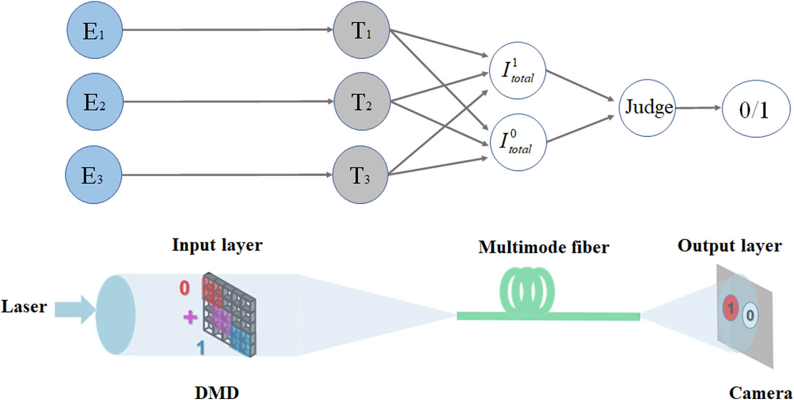
Fig. 1. Schematic diagram and the corresponding physical implementations. T i i = 1 , 2 , 3 E i I total 1 I total 0 0 + 1
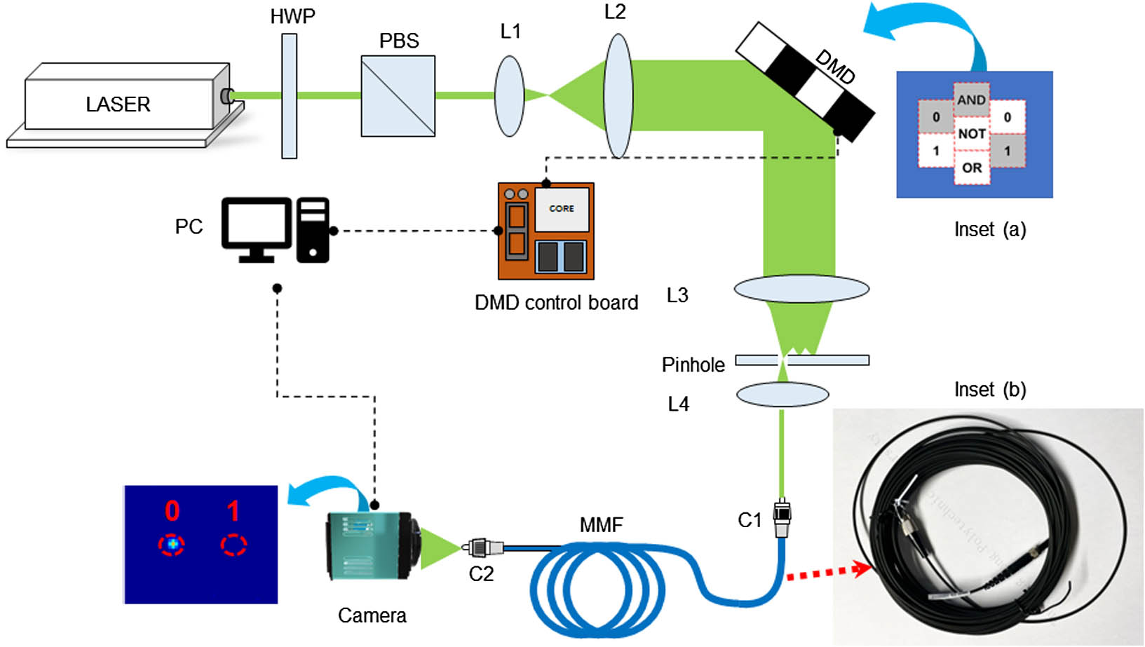
Fig. 2. Optical setup. C1, C2, collimator; DMD, digital micromirror device; HWP, half wave plate; L1–L4, lens; MMF, multimode fiber; PBS, polarization beam splitter. The figure presents a logic output state of “0” (the “0” position at the output plane, as sensed by the camera, sees an optical focus) for logic operation “0·1” (with DMD subregions 0, AND, and 1 being selected and activated), with “·” representing “AND” logic type. Inset (a) illustrates the arrangement of subregions on the DMD. Subregions around the center represent the logic type control units and the binary input digit units; subregions marked in gray represent selected and activated subregions in a specific logic operation; the subregion marked in blue serves as the common reference. Inset (b) is a photograph of the 15-m-long fiber used in this study.
Fig. 3. (a) Design arrangement of focuses formed by the seven DMD subregions individually via numerical computation. Symbol “| u | 0.5 | u | ×
Fig. 4. DMD subregion arrangement for (a) AND, (b) OR, and (c) NOT optical logic gates. Subregions marked in blue are in standby to be activated and loaded with the precalculated patterns in all logic gates. Input A is chosen from one set of binary digits (“0” or “1”) on the leftmost column, and Input B is chosen from the other set of binary digits (“0” or “1”) on the rightmost column. Q AND Q AND Q NOT
Fig. 5. Experimental results of basic logic operations. Logic gate digital output (Boolean response) for each of the four input states [(0, 0), (1, 0), (0, 1), and (1, 1) marked in blue] for (a) AND and (b) OR logic operations. (c) Logic gate digital output (Boolean response) for each of the four states [(0, NA), (NA, 0), (1, NA), and (NA, 1)] for NOT logic operations. The respective subregion inputs (blue) for each of the output states are directly related to the logic gates truth table of inputs. Digits “0” and “1” marked in yellow in (a) represent the logic states. Intensities are normalized to the maximum of each figure. “(0, NA)” marked in blue indicates that only the subregion representing input binary digit “0” on the leftmost column is selected and loaded with the precalculated pattern. Other optical logic operations in this group have similar procedures. The white curves in the upper regions in these figures are the intensity profiles across the center of the focuses.
Fig. 6. Experimental results of two logic operations (a) ( 0 + 1 ) ⋅ ( 1 ⋅ 0 ) ( 0 + 1 ) + ( 1 ⋅ 0 )
Fig. 7. Demonstration of bitwise logic operations. (a) Framework of the bitwise operations. “X” is a 6-bit operand, “Y” is the other 6-bit operand, and “L” is the logic type. Each block representing one subregion on the DMD panel. “O” is the output, which can be confirmed by identifying the light pattern captured by the camera. The direction from left to right corresponds to the bit order from the most significant bit to the least significant bit. (b) Experimental result for “bitwise AND” operation between 011010 (X) and 110101 (Y). The numbers above the focuses represent different bits. (c) Experimental result for “bitwise OR” operation between 011010 (X) and 110101 (Y). (d) Specific bitwise operation between “111100” and “000011” with a group of logic types of “AND, OR, AND, OR, OR, AND” respectively, from left to right. Solid black and dashed red arrows indicate the “0” and “1” logic state regions, respectively. Intensities are normalized to the maximum of each figure. (e)–(g) Corresponding one-dimensional intensity profiles along the “0” (black solid curve) and “1” (red dashed curve) regions in (b)–(d).
Fig. 8. (a) Simplified schematic illustration of simultaneous multiple optical logic operations. (b) Subregion arrangement on the DMD. (c) Experimental results with different linear polarization angles (π / 2 π / 4 π / 4
Fig. 9. Framework of cascaded logic gates. LG i i = 1 to n i x i 1 x i 2 y i i C i i > 2 i i + 1 C i − 1 z i C i


Set citation alerts for the article
Please enter your email address

© Copyright 2018-2021 | Chinese Laser Press. All Rights Reserved 沪ICP备15018463号-20