• Photonics Research
  • Vol. 12, Issue 3, 587 (2024)
Zhipeng Yu1、2、†, Tianting Zhong1、2、†, Huanhao Li1、2, Haoran Li1、2, Chi Man Woo1、2, Shengfu Cheng1、2, Shuming Jiao3, Honglin Liu2、4, Chao Lu5、6、7、*, and Puxiang Lai1、2、6、8、*
Author Affiliations
  • 1Department of Biomedical Engineering, The Hong Kong Polytechnic University, Hong Kong SAR, China
  • 2Hong Kong Polytechnic University Shenzhen Research Institute, Shenzhen 518000, China
  • 3Peng Cheng Laboratory, Shenzhen 518055, China
  • 4Key Laboratory for Quantum Optics, Shanghai Institute of Optics and Fine Mechanics, Chinese Academy of Sciences, Shanghai 201800, China
  • 5Department of Electronic and Information Engineering, The Hong Kong Polytechnic University, Hong Kong SAR, China
  • 6Photonics Research Institute, The Hong Kong Polytechnic University, Hong Kong SAR, China
  • 7e-mail: chao.lu@polyu.edu.hk
  • 8e-mail: puxiang.lai@polyu.edu.hk
  • show less
    DOI: 10.1364/PRJ.499523 Cite this Article Set citation alerts
    Zhipeng Yu, Tianting Zhong, Huanhao Li, Haoran Li, Chi Man Woo, Shengfu Cheng, Shuming Jiao, Honglin Liu, Chao Lu, Puxiang Lai. Long distance all-optical logic operations through a single multimode fiber empowered by wavefront shaping[J]. Photonics Research, 2024, 12(3): 587 Copy Citation Text show less

    Abstract

    Multimode fibers (MMFs) are a promising solution for high-throughput signal transmission in the time domain. However, crosstalk among different optical modes within the MMF scrambles input information and creates seemingly random speckle patterns at the output. To characterize this process, a transmission matrix (TM) can be used to relate input and output fields. Recent innovations use TMs to manipulate the output field by shaping the input wavefront for exciting advances in deep-brain imaging, neuron stimulation, quantum networks, and analog operators. However, these approaches consider input/output segments as independent, limiting their use for separate signal processing, such as logic operations. Our proposed method, which makes input/output segments as interdependent, adjusts the phase of corresponding output fields using phase bias maps superimposed on input segments. Coherent superposition enables signal logic operations through a 15-m-long MMF. In experiments, a single optical logic gate containing three basic logic functions and cascading multiple logic gates to handle binary operands is demonstrated. Bitwise operations are performed for multi-bit logic operations, and multiple optical logic gates are reconstructed simultaneously in a single logic gate with polarization multiplexing. The proposed method may open new avenues for long-range logic signal processing and transmission via MMFs.

    1. INTRODUCTION

    In the last few decades, optical fibers have seen wide applications in many fields, for example, fiber communication [1], fiber sensors [2], and optical imaging [3], due to the excellent characteristics of fibers such as ultrahigh bandwidth, anti-electromagnetic interference, low security risk, small diameter, and light weight. At the beginning, a single-mode fiber (SMF) can only support one optical mode. To improve the capacity while maintaining the compact size, few-mode fibers were developed via mode-division multiplexing [4], but the improvement of the capacity is still limited as only a few modes are supported. Comparably, multimode fiber (MMF) can support a large number of optical modes, which can be used to greatly improve the information capacity [5]. That said, when light transmits inside an MMF, the coupling of different optical modes makes the resultant signal hard to be demodulated; if coherent light is input, a randomly distributed speckle pattern is observed at the fiber output. The phenomenon is quite similar to the optical propagation inside or through a scattering medium such as ground glass and biological tissue. MMFs were initially developed to transmit digital signals in the time domain [6], and there were few attempts to transmit images through the MMF. But since 2007, the application scenarios of MMFs have been greatly extended after the proposal of wavefront shaping with the availability of spatial light modulators (SLMs) [710]. As the output light field from the MMF can be modulated arbitrarily by applying different phase and/or intensity patterns on the SLM or iteratively optimizing the input wavefront [1114], some exciting applications based on a single MMF have been inspired, such as deep-brain imaging [15], 3D holographic optical tweezer [16], single neuron stimulation [17], spectrum analyzer [18], and nonlinear multimode interactions [19]. In these applications, all input modes on the SLM serve as a whole unit and contribute to a single output target with enhanced optical energy and/or shifted wavelength, showing a single-channel signal processing task. On top of that, multi-channel signal processing can be introduced by dividing the input and output into several segments, and some more complex functionalities have been demonstrated, such as programmable optical circuits [20], linear quantum networks [21], and linear operators [22]. In these works, the input/output segments are independent, which is restricted to processing separate signals.

    Making the input/output segments interdependent can further extend this implementation to processing associated signals. To achieve this goal, in this work, a group of phase bias maps are superposed on the input segments to globally adjust the phase of the corresponding output fields, thus the coherent superposition of the desired group of output fields could make the input signals associated, and the superimposed output field can be used to recognize how the input signals are associated. That is, different superimposed output fields can be related to different association modes or associations of different input signals. In experiment, we utilize this strategy to demonstrate logic signal processing and transmission through a 15-m-long MMF simultaneously by defining the output states with binary values. To be specific, we employ a digital micromirror device (DMD, a type of SLM) loaded with precalculated wavefront patterns to modulate light before transmitting through an MMF. The DMD aperture is divided into several subregions, as illustrated in Fig. 2, that correspond to binary input digits (“0” and “1”), logic types (AND, OR, and NOT), and a common reference region, respectively. The sub-TM of the MMF corresponding to each subregion is determined by the TM-based WFS approach [23]. Two randomly selected small regions on the output plane (e.g., the camera sensor) serve as the output optical logic states “0” and “1”; light projected from each DMD subregion through the MMF can be refocused to these two regions, individually or simultaneously, with optical phases with respect to the speckle pattern projected from the common reference region on the DMD.

    As a proof of concept, built upon constructive or destructive interference among the focuses, different combinations of the subregions on the DMD loaded with precalculated wavefronts can perform different logic functions. Cascaded optical logic gates can be implemented by linking a series of logic gates with logic types placed between any two adjacent logic gates. For bitwise operators, bit-by-bit operations are performed between two 6-bit operands with the same or different logic types in parallel. Simultaneous reconstruction of multiple optical logic gates in a single logic gate with polarization multiplexing is also explored, which can be used to improve the scalability and security. With the fast development of optical wavefront shaping and optical modulators, more complex and practically useful operations could be accomplished in the near future.

    2. METHODS

    A. Working Principle

    Figure 1 illustrates the schematic and physical model of the proposed optical logic operators via an MMF. As shown, three subregions on the input layer (i.e., the DMD) are selected and marked with different colors, carrying desired wavefront patterns that represent a logic operation “0+1” in combination. Light reflected and modulated by the input layer transmits through an MMF, and the corresponding light field on the output layer can be observed and recorded by a digital camera. Two circular regions on the output layer are preselected to represent logical states “0” and “1”, respectively. As an example, with logic operation “0+1” being activated on the input layer, the output is “1”, producing an optical focus at the region corresponding to “1” (the left circle at the output layer in Fig. 1). The physical model to demonstrate the above schematic is briefed herein. Ei (i=1,2,3) is the input light field from each of the three subregions on the input layer. The transmission matrix (Ti) used to build the relationship between each input light field (Ei) and the corresponding output field on the output layer can be calculated. The optical intensities in the preselected regions can be expressed by Itotal1=(Area1TiEi)2Itotal0=(Area0TiEi)2,where Itotal1 and Itotal0 are the accumulated optical intensities in the regions “1” and “0”, respectively, on the output layer. The logic output results (Q) can be judged by the rule Q={0,Itotal1Itotal01,Itotal1Itotal0.

    Schematic diagram and the corresponding physical implementations. Ti (i=1,2,3) is the transmission matrix associated with the corresponding input light field (Ei); Itotal1 and Itotal0 are the optical intensities in regions “1” and “0”, respectively, on the output layer (Camera); “+” represents “OR” logic type. The figure presents a logic output state of “1” for logic operation “0+1”. DMD, digital micromirror device.

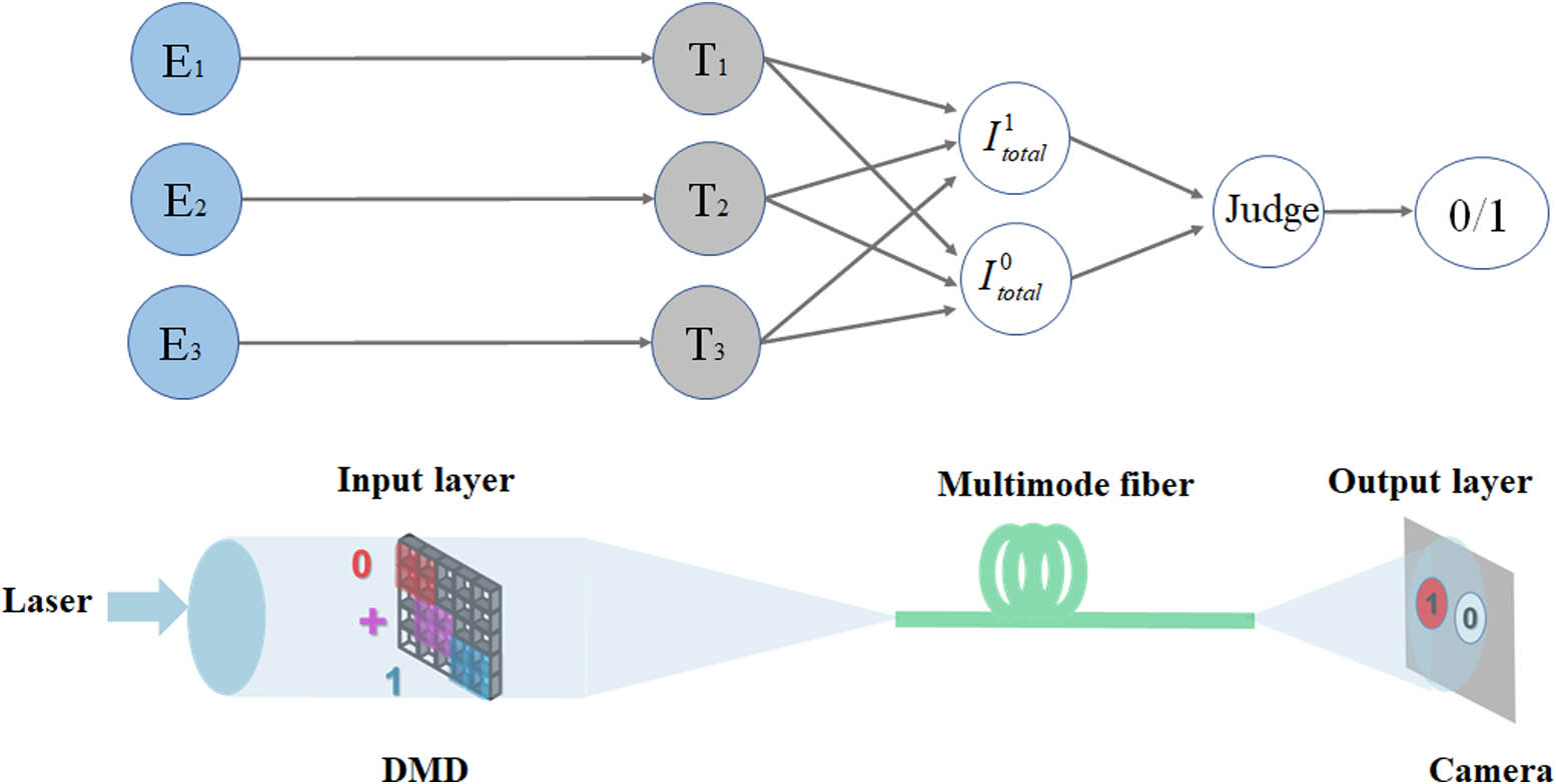
    Figure 1.Schematic diagram and the corresponding physical implementations. Ti (i=1,2,3) is the transmission matrix associated with the corresponding input light field (Ei); Itotal1 and Itotal0 are the optical intensities in regions “1” and “0”, respectively, on the output layer (Camera); “+” represents “OR” logic type. The figure presents a logic output state of “1” for logic operation “0+1”. DMD, digital micromirror device.

    The TM of the MMF is measured by scanning a two-dimensional array of optical focal spots across the proximal facet of the fiber. Each spot position is addressed by a specific diffraction grating loaded on the DMD (serving as a phase modulator) using the computer-generated off-axis hologram method [24]. More details about measurement of the TM can be referred to Ref. [23].

    The uniformity of focusing efficiency from all subregions on the DMD is critical to ensure sufficient intensity contrast for all logic operations. In experiment, however, the uneven optical illumination on the DMD and the optical coupling efficiency of different subregions into the MMF impair the uniformity. Thus, some measures need to be taken. For example, the beam pattern projected onto the DMD is adjusted to be twice the size of the DMD aperture to form a relatively even optical intensity distribution on the DMD; from any individual subregion on the DMD, the size of the scanned region on the proximal facet of the MMF is adjusted to make sure that all input channels (focal spots) within the scanned region are efficiently coupled into the MMF, which can be gauged by monitoring the output intensity from the MMF. With all these, the uniformity of focusing efficiency from all DMD subregions can be guaranteed. In the experiment, each subregion on the DMD contains 160×160 pixels. On the output plane of the MMF, a square grid consisting of 30×30 focal spots is used to achieve bright focuses of high enhancement ratio in the region of interest. Note that it is possible to obtain multiple optical focuses from different DMD subregions in the same region on the output plane, but there is no explicit phase difference among the phases of these focuses as we can only modulate the phase of the focus from individual DMD subregions separately. Since the eventual logic states are achieved based on constructive or destructive interference among different focuses generated by selected DMD subregions at the same preselected position on the output plane, bridging the phase relationship between different focuses is crucial. Therefore, the former TM measurement method is modified by introducing a common reference subregion on the DMD [the blue region in inset (a) of Fig. 2]. The reference region contains a lot more pixels (eight times larger than each working subregion) than each of the individual subregions to ensure that the reference contribution dominates in the interfered speckled field. All pixels in the reference subregion are switched “on” to project light into the MMF during the entire TM measurement process for all selected DMD subregions (control units). These pixels are switched “off” when the TM measurement is completed.

    Optical setup. C1, C2, collimator; DMD, digital micromirror device; HWP, half wave plate; L1–L4, lens; MMF, multimode fiber; PBS, polarization beam splitter. The figure presents a logic output state of “0” (the “0” position at the output plane, as sensed by the camera, sees an optical focus) for logic operation “0·1” (with DMD subregions 0, AND, and 1 being selected and activated), with “·” representing “AND” logic type. Inset (a) illustrates the arrangement of subregions on the DMD. Subregions around the center represent the logic type control units and the binary input digit units; subregions marked in gray represent selected and activated subregions in a specific logic operation; the subregion marked in blue serves as the common reference. Inset (b) is a photograph of the 15-m-long fiber used in this study.

    Figure 2.Optical setup. C1, C2, collimator; DMD, digital micromirror device; HWP, half wave plate; L1–L4, lens; MMF, multimode fiber; PBS, polarization beam splitter. The figure presents a logic output state of “0” (the “0” position at the output plane, as sensed by the camera, sees an optical focus) for logic operation “0·1” (with DMD subregions 0, AND, and 1 being selected and activated), with “·” representing “AND” logic type. Inset (a) illustrates the arrangement of subregions on the DMD. Subregions around the center represent the logic type control units and the binary input digit units; subregions marked in gray represent selected and activated subregions in a specific logic operation; the subregion marked in blue serves as the common reference. Inset (b) is a photograph of the 15-m-long fiber used in this study.

    B. Experimental Setup

    The optical setup of the proposed platform is illustrated in Fig. 2. A continuous wave laser of 532 nm wavelength (EXLSR-532-300-CDRH, Spectra Physics, USA) serves as the light source. The laser output is first expanded by a 4f system to illuminate the whole screen of the DMD (V-7001, Vialux GmbH, Germany). After being modulated and reflected by the DMD, light is shrunk by another 4f system, and then it transmits through a collimator to be focused into the MMF (length=15  m, NA=0.22, corediameter=400  μm, SUH400, XINRUI, China). At last, the output optical field from the MMF is recorded by a CMOS camera (BFS-U3-04S2M-CS, FLIR Integrated Imaging Solutions Inc., Canada), which is triggered by the DMD. In experiment, once the DMD pattern is updated, the camera will record an optical pattern.

    3. RESULTS

    A. Inverse Design

    An inverse design approach is adopted to arrange focuses on the output layer formed by the seven DMD subregions individually. First, the desired intensity and phase (0 or π) of each focus are calculated for a set of basic logic functions (AND, OR, and NOT) (the calculation process is provided in Appendix A). The solution is given in Fig. 3(a) and explained in detail in the caption. Note that two focuses of specific intensity and phase in the designated regions on the output plane should be generated synchronously from some DMD subregions with phase superposition of two corresponding phase patterns. These results are used to calculate the wavefront of each DMD subregion in reverse. The experimental verification of the design arrangement is shown in Figs. 3(b)–3(k). As mentioned earlier, two randomly picked regions on the output plane serve as logic states “0” and “1”. As an example [Fig. 3(b)], when only the subregion corresponding to “0” on the left column of the DMD (as shown in Fig. 2) is activated and loaded with the precalculated wavefront [as shown in Fig. 3(i)], two optical focuses can be observed in the selected regions [Fig. 3(b)]. Figures 3(c)–3(h) display the output images when other subregions are activated individually (one active subregion at one time) and loaded with the corresponding precalculated wavefront. As seen, all experimental results agree well with the simulated sets in Fig. 3(a). The enhancement ratio, defined as the ratio between the optimized intensity and the average intensity before optimization, is about 240 for cases with one focus [Figs. 3(d) and 3(f)]; for cases with two focuses, the enhancement ratio is in the range of 120–150. Figures 3(i)–3(k) show the precalculated binary patterns on three subregions corresponding to binary digit control units “0” (left column), “1” (right column), and logic type control unit “AND”, respectively. The intensity profiles along the central line of red circles in the upper region of Figs. 3(b), 3(c), 3(e), 3(g), and 3(h) indicate relatively balanced enhancement ratios for cases with two focuses.

    (a) Design arrangement of focuses formed by the seven DMD subregions individually via numerical computation. Symbol “|u|” represents the absolute amplitude value of the electric field of a single focus generated from individual DMD subregions, and “0.5|u|” means there is an intersection operation on the corresponding subregions, leading to dual focuses, whose absolute amplitude value of the electric field is reduced by half. “×” indicates that there is no focus formed in the designated area. “−” means that the focus is in opposite phase with the common reference; without “−” means the focus is in phase with the reference. (b)–(h) Experimental verification of the desired focus arrangement. (i)–(k) Patterns to be displayed on DMD subregions (i) “0 (left),” (j) “1 (right),” and (k) “AND,” respectively, for optical logical operation AND (0,1). The white curves in the upper regions in (b)–(h) are the intensity profiles across the center of the focuses.

    Figure 3.(a) Design arrangement of focuses formed by the seven DMD subregions individually via numerical computation. Symbol “|u|” represents the absolute amplitude value of the electric field of a single focus generated from individual DMD subregions, and “0.5|u|” means there is an intersection operation on the corresponding subregions, leading to dual focuses, whose absolute amplitude value of the electric field is reduced by half. “×” indicates that there is no focus formed in the designated area. “−” means that the focus is in opposite phase with the common reference; without “−” means the focus is in phase with the reference. (b)–(h) Experimental verification of the desired focus arrangement. (i)–(k) Patterns to be displayed on DMD subregions (i) “0 (left),” (j) “1 (right),” and (k) “AND,” respectively, for optical logical operation AND (0,1). The white curves in the upper regions in (b)–(h) are the intensity profiles across the center of the focuses.

    B. Optical Logic Gates

    The DMD subregions will display the corresponding calculated wavefronts when the subregions are selected for specific logic operations; the other subregions will be turned “off,” in which the DMD is used as a spatial switch. Figures 4(a)–4(c) show the DMD deployment for three basic optical logic gates. Inputs A and B, two binary operands, are chosen between two subregions, each representing one set of binary digits (“0” or “1”) in the leftmost column and the rightmost column, respectively. For AND and OR logic gates, Input A, Input B, and the subregion representing the corresponding logic type are activated, as shown in Figs. 4(a) and 4(b). For NOT logic gate, either Input A or Input B is activated besides the subregion representing NOT logic type, as shown in Fig. 4(c). Activated subregions will be loaded with the corresponding wavefronts that are precalculated based on the TM method discussed earlier. For a given logic operation, the logic output state (QAND, QOR, and QNOT) can be either 0 or 1.

    DMD subregion arrangement for (a) AND, (b) OR, and (c) NOT optical logic gates. Subregions marked in blue are in standby to be activated and loaded with the precalculated patterns in all logic gates. Input A is chosen from one set of binary digits (“0” or “1”) on the leftmost column, and Input B is chosen from the other set of binary digits (“0” or “1”) on the rightmost column. QAND, QAND, and QNOT, logic output states.

    Figure 4.DMD subregion arrangement for (a) AND, (b) OR, and (c) NOT optical logic gates. Subregions marked in blue are in standby to be activated and loaded with the precalculated patterns in all logic gates. Input A is chosen from one set of binary digits (“0” or “1”) on the leftmost column, and Input B is chosen from the other set of binary digits (“0” or “1”) on the rightmost column. QAND, QAND, and QNOT, logic output states.

    Experimental results of the three basic logic operations (AND, OR, and NOT) in a single logic gate are shown in Fig. 5. Switching on a desired group of subregions will result in appropriate optical logic output. As defined, if a bright focus is formed at the region representing output logic state “1” on the output plane, the logic operation registers Q=1 and vice versa. As shown, all experimental outputs for each mode behavior in Fig. 5 agree well with the required logic outputs. According to the inverse design, the desired focus intensity contrast ratios of logic operations AND (0,0) and OR (1,1) are 6 dB. For other logic operations, the contrast ratios shall be infinity as long as the focal peak-to-background ratios (PBRs) are sufficiently large to suppress the speckle background and most diffusive photons are focused onto designated regions. In our experiment, the intensity contrast ratios are 5.2 dB and 4.7 dB for logic operations AND (0,0) and OR (1,1), respectively. These are slightly lower than the designed contrast ratios, which may attribute to two aspects. First, the focusing efficiency of two focuses from the same subregions is not well-balanced. Second, the enhancement ratios are also not completely unitary at the same region on the output plane for different DMD subregions. The intensity contrast ratios of other logic operations are all more than 10 dB in our experiment. The intensity profiles along the central line of red circles in the upper region of all these figures show high intensity contrast ratios for all operations.

    Experimental results of basic logic operations. Logic gate digital output (Boolean response) for each of the four input states [(0, 0), (1, 0), (0, 1), and (1, 1) marked in blue] for (a) AND and (b) OR logic operations. (c) Logic gate digital output (Boolean response) for each of the four states [(0, NA), (NA, 0), (1, NA), and (NA, 1)] for NOT logic operations. The respective subregion inputs (blue) for each of the output states are directly related to the logic gates truth table of inputs. Digits “0” and “1” marked in yellow in (a) represent the logic states. Intensities are normalized to the maximum of each figure. “(0, NA)” marked in blue indicates that only the subregion representing input binary digit “0” on the leftmost column is selected and loaded with the precalculated pattern. Other optical logic operations in this group have similar procedures. The white curves in the upper regions in these figures are the intensity profiles across the center of the focuses.

    Figure 5.Experimental results of basic logic operations. Logic gate digital output (Boolean response) for each of the four input states [(0, 0), (1, 0), (0, 1), and (1, 1) marked in blue] for (a) AND and (b) OR logic operations. (c) Logic gate digital output (Boolean response) for each of the four states [(0, NA), (NA, 0), (1, NA), and (NA, 1)] for NOT logic operations. The respective subregion inputs (blue) for each of the output states are directly related to the logic gates truth table of inputs. Digits “0” and “1” marked in yellow in (a) represent the logic states. Intensities are normalized to the maximum of each figure. “(0, NA)” marked in blue indicates that only the subregion representing input binary digit “0” on the leftmost column is selected and loaded with the precalculated pattern. Other optical logic operations in this group have similar procedures. The white curves in the upper regions in these figures are the intensity profiles across the center of the focuses.

    After the demonstration of basic logic functions, the solution to realize cascaded optical logic gates is further pursued. Cascaded optical logic gates can be implemented by cascading a series of logic gates with logic types placed between any two adjacent logic gates; details can be referred to Appendix B. As a proof of concept, we experimentally demonstrate two logic operations by cascading two logic gates, as shown in Fig. 6. The logic output values are “0” and “1” for logic operations (0+1)    (1    0) and (0+1)+(1    0), respectively, which agree with the true values of these two operations. The intensity profiles along the central line of red circles are plotted in the upper region of the figures, whose intensity contrast ratios are 5.4 dB and 9.3 dB, respectively.

    Experimental results of two logic operations (a) (0+1) ⋅ (1 ⋅ 0) and (b) (0+1)+(1 ⋅ 0). Digits “0” and “1” marked in yellow in the figures represent the logic states. Intensities are normalized to the maximum of each figure. The white curves in the upper regions in these figures are the intensity profiles across the center of the focuses.

    Figure 6.Experimental results of two logic operations (a) (0+1)    (1    0) and (b) (0+1)+(1    0). Digits “0” and “1” marked in yellow in the figures represent the logic states. Intensities are normalized to the maximum of each figure. The white curves in the upper regions in these figures are the intensity profiles across the center of the focuses.

    C. Optical Bitwise Logic Operations

    The proposed method can be used not only to implement logic gates for single-bit operands, but also to build other kinds of operators for multi-bit operands. For demonstration, we experimentally perform 6-bit operations (“bitwise AND” and “bitwise OR”), as shown in Fig. 7. Bitwise operators perform a bit-by-bit operation on two operands. They take each bit in one operand and perform the operation with the corresponding bit in the other operand. As shown in Fig. 7(a), “X” is a 6-bit operand, “Y” is the other 6-bit operand, “L” is the logic type, and “O” is the output result. The calculation of the wavefront pattern for each subregion is quite similar to that of single-bit logic gates, except that different sets of regions representing “0” and “1” should be preselected for different bits of the operand [Fig. 7(b)]. On the output plane, there are six regions in both the upper region (solid arrow) and the lower region (dashed arrow) to represent for “0” and “1” for each bit, and the numbers (0–5) correspond to the bit positions of the output. For example, Fig. 7(b) shows the experimental result of “010000” for “bitwise AND” operation between 011010 (X) and 110101 (Y), which agrees well with the true value; Fig. 7(c) shows the experimental result of “110111” for “bitwise OR” operation between 010101 (X) and 100010 (Y). Furthermore, it is possible to implement different functions for different bits by assigning them with different logic types. For example, an operand (X) “111100” can be combined with another operand (Y) “000011” via a group of logic types of “AND, OR, AND, OR, OR, AND,” respectively, to implement “bit-set” in the second bit, “bit-clear” in the fourth and sixth bits, and “bit-check” in other bits. As shown in Fig. 7(d), by recognizing the locations of the focuses, a result of “010110” is output, which is consistent with the desired value. The intensity profiles along the “0” and “1” regions between the solid and dashed arrows in Figs. 7(b)–7(d) are also plotted in Figs. 7(e)–7(g), respectively, showing high intensity contrast ratios for all bitwise operations.

    Demonstration of bitwise logic operations. (a) Framework of the bitwise operations. “X” is a 6-bit operand, “Y” is the other 6-bit operand, and “L” is the logic type. Each block representing one subregion on the DMD panel. “O” is the output, which can be confirmed by identifying the light pattern captured by the camera. The direction from left to right corresponds to the bit order from the most significant bit to the least significant bit. (b) Experimental result for “bitwise AND” operation between 011010 (X) and 110101 (Y). The numbers above the focuses represent different bits. (c) Experimental result for “bitwise OR” operation between 011010 (X) and 110101 (Y). (d) Specific bitwise operation between “111100” and “000011” with a group of logic types of “AND, OR, AND, OR, OR, AND” respectively, from left to right. Solid black and dashed red arrows indicate the “0” and “1” logic state regions, respectively. Intensities are normalized to the maximum of each figure. (e)–(g) Corresponding one-dimensional intensity profiles along the “0” (black solid curve) and “1” (red dashed curve) regions in (b)–(d).

    Figure 7.Demonstration of bitwise logic operations. (a) Framework of the bitwise operations. “X” is a 6-bit operand, “Y” is the other 6-bit operand, and “L” is the logic type. Each block representing one subregion on the DMD panel. “O” is the output, which can be confirmed by identifying the light pattern captured by the camera. The direction from left to right corresponds to the bit order from the most significant bit to the least significant bit. (b) Experimental result for “bitwise AND” operation between 011010 (X) and 110101 (Y). The numbers above the focuses represent different bits. (c) Experimental result for “bitwise OR” operation between 011010 (X) and 110101 (Y). (d) Specific bitwise operation between “111100” and “000011” with a group of logic types of “AND, OR, AND, OR, OR, AND” respectively, from left to right. Solid black and dashed red arrows indicate the “0” and “1” logic state regions, respectively. Intensities are normalized to the maximum of each figure. (e)–(g) Corresponding one-dimensional intensity profiles along the “0” (black solid curve) and “1” (red dashed curve) regions in (b)–(d).

    D. Simultaneous Multiple Logic Operations with Polarization Multiplexing

    The proposed method is also explored for simultaneous multiple optical logic operations with a single logic gate. As shown in Fig. 8(a), with the same set of input digits, the system can output two logic operations (OR and AND) in different output polarization channels. In experiment, a linear polarizer is put behind the MMF to change the polarization state of the speckles. Two TMs (v-TM and p-TM) are measured when the polarization is vertical (π/2) and parallel (0) to the horizontal plane, respectively. The wavefronts displayed on each subregion for OR and AND operations are calculated according to v-TM and p-TM, respectively. Two sets of wavefronts are superimposed and displayed on the corresponding subregions as shown in Fig. 8(b). The experimental results are demonstrated in Fig. 8(c) when the polarization angle takes different values. As shown, when the polarization angle is π/2, OR operations are performed; when the polarization angle is 0, AND operations are performed; and when the polarization angle is π/4, chaotic information is obtained with these two kinds of operations mixed. Such simultaneous construction of multiple logic operations in a single logic gate with polarization multiplexing can be used to extend the scalability and enhance the security of the system.

    (a) Simplified schematic illustration of simultaneous multiple optical logic operations. (b) Subregion arrangement on the DMD. (c) Experimental results with different linear polarization angles (π/2, 0, and π/4) are demonstrated individually in different rows. Four input states (0, 0), (1, 0), (0, 1), and (1, 1) are marked in blue. The encircled regions in the first figure represent the expression of logic states: if an optical focus is only formed at “0” position, it suggests an output of “0” from the logic operation; if an optical focus is only formed at “1” position, it suggests an output of “1” from the logic operation; if focuses are formed at both “0” and “1” positions, as the central examples with polarization angle of π/4, it suggests an invalid or unpredictable output.

    Figure 8.(a) Simplified schematic illustration of simultaneous multiple optical logic operations. (b) Subregion arrangement on the DMD. (c) Experimental results with different linear polarization angles (π/2, 0, and π/4) are demonstrated individually in different rows. Four input states (0, 0), (1, 0), (0, 1), and (1, 1) are marked in blue. The encircled regions in the first figure represent the expression of logic states: if an optical focus is only formed at “0” position, it suggests an output of “0” from the logic operation; if an optical focus is only formed at “1” position, it suggests an output of “1” from the logic operation; if focuses are formed at both “0” and “1” positions, as the central examples with polarization angle of π/4, it suggests an invalid or unpredictable output.

    4. DISCUSSION

    In this study, we have proposed the concept and working principle to achieve different optical logic operations, including basic logic gates and bitwise operations, with a single MMF empowered by TM-based wavefront shaping. In the proposed logic operators, the output states are recognized by the intensity contrast between two preselected regions that respectively represent logical states “0” and “1” on the output plane. With this MMF-based logic system, analog-to-digital and digital-to-analog conversions can be essentially avoided, especially when the camera is replaced with photoelectric detectors. Currently, the measurement of each sub-TM takes 7.2  s, which is mainly restricted by the working frame rate (500 Hz) of the camera used in the system. One effective way to shorten this duration is to adopt a faster detector, such as a photoelectric detector [25], which could reduce the measurement time down to 160  ms. This kind of task through MMF cannot be completed by traditional optical logic components based on waveguides [2632] or metasurfaces [33,34] without reconfiguration, and in the meantime our proposed method exhibits some unique features or advantages. To begin with, different logic functions can be obtained by switching the modulating patterns on the SLM, as long as the TM of the MMF is calculated. In addition, under conditions when the MMF is considerably perturbed causing large variations to the TM of the MMF in real-world applications, TMs of MMF under plenty of perturbation conditions can be measured in advance and utilize the light field reflected by the distal end of the MMF in the proximal end to screen out the suitable TM [35]. Installing a series of controlled units on the MMF surface directly to locally adjust the MMF status with much faster speed will be a good alternative solution to improve the speed and in the meantime decrease the complexity of the optical setup [36]. As a proof of concept, in this paper, we demonstrate 6-bit bitwise operations; the bit length is mainly limited by the pixel number on the DMD (1024×768) used in experiment while guaranteeing the accuracy of each logic output. But our results show that the crosstalk among different parallel channels in bitwise operations is quite low, which means the method can be potentially extended to more bit operations when a DMD with a larger number of pixels is adopted. For example, if the merged pixel number in each subregion is kept at 160×160, which is the same as that in this paper, the maximum number of parallel channels (480×160 pixels for each parallel channel, which contains three subregions) can be as large as 104 using a new DMD that has a large number of pixels up to 3840×2160 (DLP660TE, Texas Instruments).

    Energy consumption is another critical concern for a computing system. Since the sub-TMs are retrieved and all patterns to be loaded on the DMD subregions are determined in advance, the logic operations are actually performed in a single shot in a passive system, and no further calibration is needed as long as the optical system is moderately stable. Within this duration, the laser, DMD, and detectors should be in charge to complete the task. Notably, the energy consumption will not increase with the increase of logic operations if these logic operations can be performed within a DMD. In addition, in our work, different logic functions are obtained by switching on the corresponding subregions on the DMD. The speed is limited by the update rate of DMD, which can be further accelerated using other components such as an acousto-optic deflector (AOD) [23]. Stability over a long time can be obtained by packing the MMF carefully [37]. For example, high-speed image projection through a 200-m unfixed MMF with a duration of 5 days was recently reported by using single point feedback in the proximal end [35]. The work can also provide inspirations for our method to adapt to the environment perturbations.

    It also should be noted that, although only basic functions such as AND, OR, and NOT are demonstrated in the study, the concept can be extended for the remaining logic gates, such as NAND, NOR, XAND, and XOR [38], and other operators including arithmetic, relational, equality, reduction, shift, concatenation, and conditional [39] with appropriate modifications. To achieve these extensions, in experiment, the amplitude of the focus is assigned with three values at 0, 0.5u, and u, and the phase of the focus is assigned with values of 0 and π. To extend the method to other logic operations, the amplitude and phase of the focus are needed to take more values. This procedure is feasible in existing optical systems with more accurate adjustment: the amplitude can be tuned accurately by controlling the “open” pixel number in each subregion; the phase of the focus can be set to an arbitrary value from 0 to 2π with respect to the common reference light field as we use a DMD to modulate the phase of the light field. More values of output states can be introduced with more precise modulation, and thus this method can be furtherly used for operations among operands of high bases such as quaternary and octonary operands. These logic operations are performed in the spatial domain, which can be potentially combined with other optical fiber multiplexing techniques, such as optical time division multiplexing (OTDM) [40] and wavelength division multiplexing (WDM) [41], for the purpose of signal transmission and processing.

    Last but not least, it is also worthwhile to highlight that it is nearly impossible for hackers to steal the useful signals/information from our system due to the inherently anti-eavesdropping feature. Stealers cannot decipher the carried signals but only obtain unintelligible contents when intercepting the signals at a position between the proximal end and the distal end of the MMF as signals associated with the TMs vary dramatically at different positions along the MMF. This encryption method is inherent due to the optical transmission process inside MMF and can be enhanced by specifically modulating the polarization of the output field in the output terminal. Even hackers can obtain access to the MMF; they have to decipher the polarization first in order to decode the logic signals. The proposed method can be combined with information encryption means in the input terminal such as symmetric-key algorithm and asymmetric-key encryption. Thus, the proposed schematic may function as a device that is able to simultaneously transmit and process optical logic signals in a highly encrypted way. Also, the transmission matrix (TM) of an MMF is wavelength-dependent because optical modes inside MMF are wavelength sensitive. Adopting the procedure similar to the parallel computation with polarization multiplexing, different logic functions can be designed into different wavelength channels; individual wavefront patterns can be superimposed and displayed on the corresponding subregions to achieve simultaneous multiple logic operations with wavelength multiplexing. Besides, the strategy proposed in this work can be extended to fiber bundles, as controlling the phase of light of each core in the proximal end of fiber bundles via SLM will similarly induce variations to the output light field from the fiber bundle [42].

    5. CONCLUSION

    To conclude, optical logic signal processing and transmission through a 15-m-long MMF based on TM-based wavefront shaping are proposed and demonstrated in this work. Light is first modulated by a DMD loaded with predetermined modulation patterns and then transmits through an MMF to output logic states. By choosing a common reference speckle field for light reflected from seven DMD subregions, the study has experimentally demonstrated the feasibility and robustness of basic logic functions, cascaded logic operations, as well as bitwise operations for multiple bits of operands. Finally, simultaneous reconstruction of multiple optical logic gates in a single logic gate with polarization multiplexing is also explored, which provides a solution to the improvement of the integration and security of the system. Whilst the performance, such as the speed of precalibration, can be further engineered in the next phase, the proposed method empowers reconfigurable optical logic processing capability via MMFs, which has not been demonstrated by any existing implementations in the field. The capability may also find or benefit wide applications in long-distance optical information transmission and encryption.

    APPENDIX A: PHASE AND INTENSITY CALCULATION OF FOCUSES

    Characters “a” to “n” represent the electric field amplitude of focuses generated by the seven DMD subregions/control units (see Table 1). The combination of different groups can act as different logic operations. And their relationship should obey the below inequations: |a+c+e|2|h+j+l||a+c+f|2|h+j+m|2|a+g||h+n||a+d+e|2|h+k+l|2|a+d+f||h+k+m||b+g|2|i+n||b+c+e|2|i+j+l|2|b+c+f||i+j+m|2|c+g||j+n|2|b+d+e||i+k+l|2|b+d+f||i+k+m||d+g|2|k+n|.

    If a character is negative, the phase of the corresponding focus is π (in opposite phase with the reference); if a character is positive, the phase of the corresponding focus is 0 (in phase with the reference). The threshold setting is that if logic output is “0”, the absolute amplitude value of the synthetic field in the region of logical state “0” should be twice larger than that in the region of logical state “1”, and vice versa.

    Desired Phases and Intensities of Focuses from Each DMD Subregion in an Inverse Designa

    0 (left)1 (left)0 (right)1 (right)ANDORNOT
    “0”abcdefg
    “1”hijklmn

    Characters “a” to “n” are the required electric field amplitudes of the focuses at the focal regions representing logic states “0” and “1”. If the character is negative, the focus is in opposite phase with respect to the reference; otherwise, the focus is in phase with the reference.

    APPENDIX B: CASCADED LOGIC GATES

    As mentioned in the main text, we can cascade Logic Gates 1 (LG1) and 2 (LG2) by connecting the output light fields of them, which serves as inputs to a connector (C1) consisting of different logic types. Logic Gate 3 (LG3) can be included in the cascaded system by connecting the output field of the first two cascaded logic gates and the output field of LG3 to another connector (C2). With similar procedures, more logic gates can be cascaded. Note that, however, this framework requires a calibration procedure. If each transitional output field [yi(i=1  to  n), zi(i=1  to  n2)] can be calibrated to equal the output field of the initial input digit (xi1 and xi2) with the same value as shown in Fig. 9, the whole design of the cascaded system will be the same as that of the basic logic functions.

    Framework of cascaded logic gates. LGi (i=1 to n) is the ith logic gate; xi1 and xi2 are the two inputs of the corresponding logic gate; yi is the logic output of the ith logic gate; Ci (i>2) is the ith connector consisting of different logic types connecting the (i+1)th logic gate and the output of Ci−1; zi is the output from the corresponding connector Ci.

    Figure 9.Framework of cascaded logic gates. LGi (i=1  to  n) is the ith logic gate; xi1 and xi2 are the two inputs of the corresponding logic gate; yi is the logic output of the ith logic gate; Ci (i>2) is the ith connector consisting of different logic types connecting the (i+1)th logic gate and the output of Ci1; zi is the output from the corresponding connector Ci.

    Four output states for each logic gate and the corresponding logic functions are: [(2|u|,|u|): AND(0,0)], [(|u|,2|u|): OR(1,1)], [(|u|,0): AND(0,1), AND(1,0), OR(0,0)], and [(0,|u|): OR(0,1), OR(1,0), AND(1,1)]. As a proof of concept, a calibration block with an output field of (0.5|u|, 0.5|u|) will be added onto the output of the logic gate. As seen, apart from two logical operations AND(0,0) and OR(1,1) with calibrated results of (1.5|u|, 1,5|u|) and (1.5|u|,-1,5|u|), respectively, calibrated results of other logic operations are the same as that of the initial corresponding input values [(0.5|u|, 0.5|u|) and (0.5|u|, 0.5|u|)]. If additional calibrations are not applied on these two special logic operations, AND(0,0) and OR(1,1), the contrast of the output field becomes worse with the increase of the number of the logic gates. We have introduced a precondition in the system for these two logic operations. When performing AND(0,0) and OR(1,1), two additional blocks with output fields of (|u|,|u|) and (|u|,|u|) will be introduced, respectively, to make the calibrated results of these two logic operations be the same as those of the initial corresponding input values. In future work, more values of the intensity and phase of the output field will be taken and more accurate inverse design will be adopted, so that the precondition can be avoided.

    References

    [1] K. Zhong, X. Zhou, T. Gui. Experimental study of PAM-4, CAP-16, and DMT for 100 Gb/s short reach optical transmission systems. Opt. Express, 23, 1176-1189(2015).

    [2] T. G. Giallorenzi, J. A. Bucaro, A. Dandridge. Optical fiber sensor technology. IEEE Trans. Microwave Theory Tech., 30, 472-511(1982).

    [3] B. A. Flusberg, E. D. Cocker, W. Piyawattanametha. Fiber-optic fluorescence imaging. Nat. Methods, 2, 941-950(2005).

    [4] N. Bai, E. Ip, Y.-K. Huang. Mode-division multiplexed transmission with inline few-mode fiber amplifier. Opt. Express, 20, 2668-2680(2012).

    [5] M. W. Matthès, Y. Bromberg, J. de Rosny. Learning and avoiding disorder in multimode fibers. Phys. Rev. X, 11, 021060(2021).

    [6] D. C. Gloge, T. Li. Multimode-fiber technology for digital transmission. Proc. IEEE, 68, 1269-1275(1980).

    [7] I. M. Vellekoop, A. Mosk. Focusing coherent light through opaque strongly scattering media. Opt. Lett., 32, 2309-2311(2007).

    [8] Z. Yu, H. Li, T. Zhong. Wavefront shaping: a versatile tool to conquer multiple scattering in multidisciplinary fields. Innovation, 3, 100292(2022).

    [9] S. Cheng, T. Zhong, C. M. Woo. Alternating projection-based phase optimization for arbitrary glare suppression through multimode fiber. Opt. Laser Eng., 161, 107368(2023).

    [10] H. Li, Z. Yu, Q. Zhao. Learning-based super-resolution interpolation for sub-Nyquist sampled laser speckles. Photon. Res., 11, 631-642(2023).

    [11] M. Plöschner, T. Tyc, T. Čižmár. Seeing through chaos in multimode fibres. Nat. Photonics, 9, 529-535(2015).

    [12] Y. Choi, C. Yoon, M. Kim. Scanner-free and wide-field endoscopic imaging by using a single multimode optical fiber. Phys. Rev. Lett., 109, 203901(2012).

    [13] A. M. Caravaca-Aguirre, E. Niv, D. B. Conkey. Real-time resilient focusing through a bending multimode fiber. Opt. Express, 21, 12881-12887(2013).

    [14] S. Cheng, T. Zhong, C. M. Woo. Long-distance pattern projection through an unfixed multimode fiber with natural evolution strategy-based wavefront shaping. Opt. Express, 30, 32565-32576(2022).

    [15] S. A. Vasquez-Lopez, R. Turcotte, V. Koren. Subcellular spatial resolution achieved for deep-brain imaging in vivo using a minimally invasive multimode fiber. Light Sci. Appl., 7, 110(2018).

    [16] I. T. Leite, S. Turtaev, X. Jiang. Three-dimensional holographic optical manipulation through a high-numerical-aperture soft-glass multimode fibre. Nat. Photonics, 12, 33-39(2017).

    [17] T. Zhong, Z. Qiu, Y. Wu. Optically selective neuron stimulation with a wavefront shaping‐empowered multimode fiber. Adv. Photon. Res., 3, 2100231(2022).

    [18] B. Redding, M. Alam, M. Seifert. High-resolution and broadband all-fiber spectrometers. Optica, 1, 175-180(2014).

    [19] O. Tzang, A. M. Caravaca-Aguirre, K. Wagner. Adaptive wavefront shaping for controlling nonlinear multimode interactions in optical fibres. Nat. Photonics, 12, 368-374(2018).

    [20] S. R. Huisman, T. J. Huisman, T. A. W. Wolterink. Programmable multiport optical circuits in opaque scattering materials. Opt. Express, 23, 3102-3116(2015).

    [21] S. Leedumrongwatthanakun, L. Innocenti, H. Defienne. Programmable linear quantum networks with a multimode fibre. Nat. Photonics, 14, 139-142(2020).

    [22] M. W. Matthès, P. del Hougne, J. de Rosny. Optical complex media as universal reconfigurable linear operators. Optica, 6, 465-472(2019).

    [23] M. Plöschner, B. Straka, K. Dholakia. GPU accelerated toolbox for real-time beam-shaping in multimode fibres. Opt. Express, 22, 2933-2947(2014).

    [24] W.-H. Lee. Binary computer-generated holograms. Appl. Opt., 18, 3661-3669(1979).

    [25] H. Yu, K. Lee, Y. Park. Ultrahigh enhancement of light focusing through disordered media controlled by mega-pixel modes. Opt. Express, 25, 8036-8047(2017).

    [26] H. Wei, Z. Li, X. Tian. Quantum dot-based local field imaging reveals plasmon-based interferometric logic in silver nanowire networks. Nano Lett., 11, 471-475(2011).

    [27] Q. Xu, M. Lipson. All-optical logic based on silicon micro-ring resonators. Opt. Express, 15, 924-929(2007).

    [28] P. Zhou, L. Zhang, Y. Tian. 10 GHz electro-optical OR/NOR directed logic device based on silicon micro-ring resonators. Opt. Lett., 39, 1937-1940(2014).

    [29] Y. Tian, Y. Zhao, W. Chen. Electro-optic directed XOR logic circuits based on parallel-cascaded micro-ring resonators. Opt. Express, 23, 26342-26355(2015).

    [30] C. Yao, A. Kotb, B. Wang. All-optical logic gates using dielectric-loaded waveguides with quasi-rhombus metasurfaces. Opt. Lett., 45, 3769-3772(2020).

    [31] Y. Sang, X. Wu, S. S. Raja. Broadband multifunctional plasmonic logic gates. Adv. Opt. Mater., 6, 1701368(2018).

    [32] T. Sadeghi, S. Golmohammadi, A. Farmani. Improving the performance of nanostructure multifunctional graphene plasmonic logic gates utilizing coupled-mode theory. Appl. Phys. B, 125, 189(2019).

    [33] C. Qian, X. Lin, X. Lin. Performing optical logic operations by a diffractive neural network. Light Sci. Appl., 9, 59(2020).

    [34] M. Manjappa, P. Pitchappa, N. Singh. Reconfigurable MEMS Fano metasurfaces with multiple-input–output states for logic operations at terahertz frequencies. Nat. Commun., 9, 4056(2018).

    [35] Z. Wen, Z. Dong, C. Pang. Single multimode fiber for in vivo light-field encoded nano-imaging. arXiv(2022).

    [36] S. Resisi, Y. Viernik, S. M. Popoff. Wavefront shaping in multimode fibers by transmission matrix engineering. APL Photon., 5, 036103(2020).

    [37] T. H. Chan, L. Yu, H.-Y. Tam. Fiber Bragg grating sensors for structural health monitoring of Tsing Ma bridge: background and experimental observation. Eng. Struct., 28, 648-659(2006).

    [38] X. Tang, Y. Zhai, L. Sun. Implementation of a reconfigurable optical logic gate using a single I/Q modulator with direct detection. IEEE Photon. J., 8, 7802808(2016).

    [39] S. Palnitkar. Verilog HDL: A Guide to Digital Design and Synthesis, 1(2003).

    [40] H. G. Weber, R. Ludwig, S. Ferber. Ultrahigh-speed OTDM-transmission technology. J. Lightwave Technol., 24, 4616-4627(2007).

    [41] S. J. Park, C. H. Lee, K. T. Jeong. Fiber-to-the-home services based on wavelength-division-multiplexing passive optical network. J. Lightwave Technol., 22, 2582-2591(2004).

    [42] A. Porat, E. R. Andresen, H. Rigneault. Widefield lensless imaging through a fiber bundle via speckle correlations. Opt. Express, 24, 16835-16855(2016).

    Zhipeng Yu, Tianting Zhong, Huanhao Li, Haoran Li, Chi Man Woo, Shengfu Cheng, Shuming Jiao, Honglin Liu, Chao Lu, Puxiang Lai. Long distance all-optical logic operations through a single multimode fiber empowered by wavefront shaping[J]. Photonics Research, 2024, 12(3): 587
    Download Citation