
Siqi Yan, Yan Zuo, Sanshui Xiao, Leif Katsuo Oxenløwe, Yunhong Ding. Graphene photodetector employing double slot structure with enhanced responsivity and large bandwidth[J]. Opto-Electronic Advances, 2022, 5(12): 210159
- Opto-Electronic Advances
- Vol. 5, Issue 12, 210159 (2022)
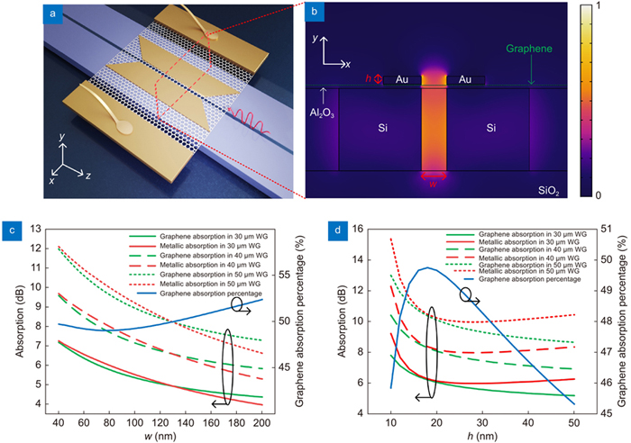
Fig. 1. (a ) 3D schematic of the proposed photodetector based on the double slot structure. The red dashed region indicates the core part of the double slot structure. (b ) The normalized x-direction distribution of the electrical field within the cross section of the core part of the double slot structure. The height (h) of the Au is set as 25 nm while the gap (w) width is set as 80 nm. (c ) Theoretical calculation results of the graphene absorption (green curve), metallic absorption (red curve) and graphene absorption percentage (blue curve) as a function of w under different waveguide (WG) lengths, when the h is set as 25 nm. (d ) The graphene absorption (green curve), metallic absorption (red curve) and graphene absorption percentage (blue curve) as a function of h under different waveguide (WG) lengths, when the w is set as 80 nm.
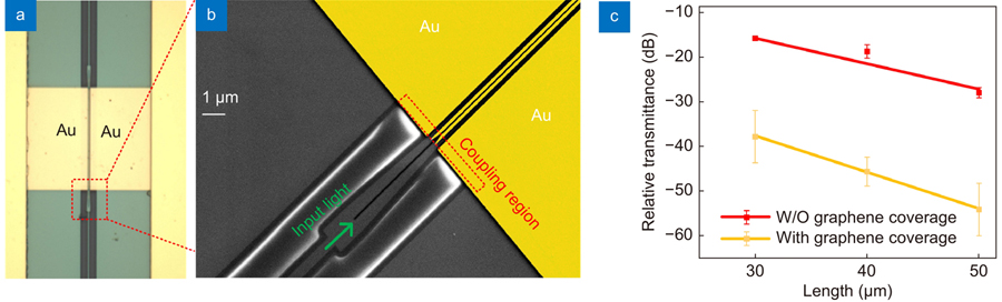
Fig. 2. (a ) Microscopic image of the double slot graphene photodetector. (b ) SEM image of the zoom-in region of the double slot structure. (c ) Measured relative transmittance of the double slot structure with (yellow dots and curve) and without graphene (red dots and curve) coverage.
Fig. 3. (a ) The measured I-V curve of the proposed device. Blue curve is the case when there is no light illumination, while the red curve is the case when there is light illumination. (b ) Zoom-in view of the I-V curve with the bias voltage from 1.4 V to 2.0 V. (c ) Zoom-in view of the I-V curve with the bias voltage from −1.9 V to −1.4 V. (d ) The relationship between the photocurrent and the bias voltage when the input optical power is 0.386 mW. (e ) The responsivity as a function of the input optical power when the applied bias voltage is 1.9 V. (f ) The maximum responsivity obtained with different lengths.
Fig. 4. The frequency response obtained by VNA (yellow curve) and FB (green curve) for the devices with detection length of (a ) 30 μm, (b ) 40 μm, and (c ) 50 μm. The inset shows both the eye diagrams of the received 10 Gbit/s and 15 Gbit/s optical NRZ signal.
Fig. 5. (a ) The metallic absorption caused by the metal contact pad as a function of its position. (b ) The graphene and metallic absorption coefficients as a function of the gap width (w) of the double slot waveguide using mainstream SOI substrates with different top silicon layer thicknesses. Solid line: 260 nm top silicon layer. Dashed line: 250 nm top silicon layer. Dash-dot line: 220 nm top silicon layer. (c ) The absorption variation as a function of the misalignment. The inset figure shows the optical mode distribution when the misalignment is 40 nm. The purple curve represents the variation of graphene absorption while the brown curve represents the variation of metallic absorption. (d ) Graphene absorption coefficient as a function of the gap width (w) under different filling materials in the slot when the h is 25 nm.
|
Table 1. The comparison of the key figure of merits of the integrated photodetector working at 1550 nm.


Set citation alerts for the article
Please enter your email address

© Copyright 2018-2021 | Chinese Laser Press. All Rights Reserved 沪ICP备15018463号-20