Abstract
Silicon photonics integrated with graphene provides a promising solution to realize integrated photodetectors operating at the communication window thanks to graphene’s ultrafast response and compatibility with CMOS fabrication process. However, current hybrid graphene/silicon photodetectors suffer from low responsivity due to the weak light-graphene interaction. Plasmonic structures have been explored to enhance the responsivity, but the intrinsic metallic Ohmic absorption of the plasmonic mode limits its performance. In this work, by combining the silicon slot and the plasmonic slot waveguide, we demonstrate a novel double slot structure supporting high-performance photodetection, taking advantages of both silicon photonics and plasmonics. With the optimized structural parameters, the double slot structure significantly promotes graphene absorption while maintaining low metallic absorption within the double slot waveguide. Based on the double slot structure, the demonstrated photodetector holds a high responsivity of 603.92 mA/W and a large bandwidth of 78 GHz. The high-performance photodetector provides a competitive solution for the silicon photodetector. Moreover, the double slot structure could be beneficial to a broader range of hybrid two-dimensional material/silicon devices to achieve stronger light-matter interaction with lower metallic absorption.Silicon photonics integrated with graphene provides a promising solution to realize integrated photodetectors operating at the communication window thanks to graphene’s ultrafast response and compatibility with CMOS fabrication process. However, current hybrid graphene/silicon photodetectors suffer from low responsivity due to the weak light-graphene interaction. Plasmonic structures have been explored to enhance the responsivity, but the intrinsic metallic Ohmic absorption of the plasmonic mode limits its performance. In this work, by combining the silicon slot and the plasmonic slot waveguide, we demonstrate a novel double slot structure supporting high-performance photodetection, taking advantages of both silicon photonics and plasmonics. With the optimized structural parameters, the double slot structure significantly promotes graphene absorption while maintaining low metallic absorption within the double slot waveguide. Based on the double slot structure, the demonstrated photodetector holds a high responsivity of 603.92 mA/W and a large bandwidth of 78 GHz. The high-performance photodetector provides a competitive solution for the silicon photodetector. Moreover, the double slot structure could be beneficial to a broader range of hybrid two-dimensional material/silicon devices to achieve stronger light-matter interaction with lower metallic absorption.Introduction
The ongoing fourth industrial revolution is data-driven1 and heavily relies on the data communication and telecommunication system capacity to deal with the explosive data increase2. The optical interconnects are expected to feature higher bandwidth, smaller footprint, and lower power consumption to meet the dramatically growing demand for stronger data processing ability3, 4. Silicon photonics provides an ideal solution for the fully integrated optical interconnects thanks to its low loss, low cost, and compatibility with the mature Complementary Metal-Oxide-Semiconductor (CMOS) technology5-7. Impressive progress has been achieved on the silicon platform, including ultrahigh-speed modulator8, 9, on-chip silicon laser10, phase shifter with ultralow power consumption11 and quantum technology12, 13. However, owing to its transparency in the wavelength near 1.55 μm, it is challenging to realize high-performance photodetection only based on pure silicon (Si), which mainly relies on defect-mediated absorption, two-photon absorption, and the internal photoemission effect14. Thus, various materials have been introduced to be hybrid integrated with silicon to act as photon absorption medium, and the most reported materials are germanium (Ge) and graphene. Ge/Si photodetector exhibits modest performance and has been widely investigated15, 16. Meanwhile, graphene/Si photodetector holds more potential than Ge/Si photodetector thanks to graphene’s extraordinary properties, including ultrahigh carrier mobility17 and its gapless energy band structure18. Based on these properties, the graphene photodetectors have attracted considerable attention since the first demonstration19. Impressive performances such as ultrahigh bandwidth over 100 GHz, operation wavelength covering from 1.55 μm to 2 μm and polarization division multiplexing detection have been experimentally verified20-23. However, owing to the atomic thickness of monolayer graphene, the light-graphene interaction is seriously limited, thus significantly impairing the responsivity of graphene/Si photodetectors. Plasmonic structures24, 25 are widely utilized to enhance the responsivity, but the intrinsic metallic loss of the plasmonic mode is normally higher than 0.5 dB/μm23, 26-28, which inevitably poses obstacles in reaching high-performance photodetectors. Here, we demonstrate a novel double slot structure to simultaneously realize high responsivity and large bandwidth of the graphene/Si hybrid photodetector, of which the preliminary results were previously reported29. With the optimized structure of the photodetector, the metallic absorption is significantly reduced, while the maximum responsivity of 603.92 mA/W with the bandwidth of 78 GHz is reached. Meanwhile, the novel double slot structure provides a promising path to realize stronger light-matter interaction with low metallic Ohmic absorption for hybrid integration of two-dimensional materials and integrated photonics circuits30, including lasers31, 32, modulators33, 34, and other optoelectronic applications35-37.
Device design and fabrication
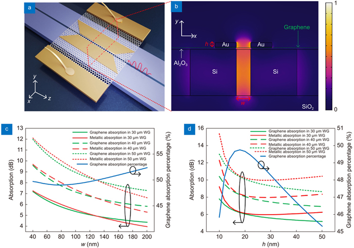
Silicon slot waveguide enabling the localization of light within tens of nanometers scale with low propagation loss, has been extensively used within optical modulators38, optical switch39, dispersion engineering40 and optical sensing41. The responsivity of graphene photodetector based on silicon slot is reported to be 0.273 A/W42, while the bandwidth is limited around 20 kHz. In order to both further increase the light-matter interaction and reach high operation bandwidth, graphene-plasmonic hybrid structures have been widely proposed43. Unfortunately, up to 54% of the input light is absorbed by the metallic structure21, which does not contribute to the photocurrent, thus significantly lower the responsivity. In order to address this issue, we propose a novel graphene-silicon hybrid photodetector with double slot structure to balance the metallic absorption and the light-graphene interaction. The schematic of the double slot structure is displayed in Fig. 1(a). The core part of the photodetector consists of two slot waveguides with different materials: a silicon slot waveguide and a gold (Au) slot waveguide, which have the same gap width (w). The material filled in the silicon slot waveguide is SiO2, while air is filled in the Au slot waveguide. Al2O3 with 7 nm thickness is introduced above the silicon slot waveguide and titanium (Ti) with 3 nm thickness is employed as an adhesion layer under Au plasmonic waveguide. Monolayer graphene is sandwiched between the Au plasmonic slot waveguide and the silicon slot waveguide as the absorption medium. The normalized electric field's x-direction distribution within the structure is displayed in Fig. 1(b), where one could find that a light is mostly confined within the double slot. To determine the structural parameters, the graphene absorption and metallic absorption under different gap width (w) and Au height (h) using COMSOL Multiphysics (See Supplementary information). In Fig. 1(c), one could see that narrower gap width leads to higher absorption in both graphene (green curve) and metal (red curve), owing to the stronger light confinement within the double slot. Considering the fabrication limitation, the slot width is set as 80 nm. It should be noted that when the gap width is 80 nm, the graphene absorption percentage (blue curve) is calculated to be 49 %, which is slightly lower than its maximum value of 52 %. However, the absolute graphene absorption remains significantly higher than the case with wider gap, which will contribute to higher responsivity. As the Fig. 1(d) shows, the graphene absorption decreases with the increase of the h, while the metallic absorption reaches its minimum with h around 25 nm. Therefore, to obtain the highest possible absorption within graphene and lowest metallic absorption in our design, the height of the Au is set as 25 nm. Meanwhile, the graphene absorption percentage remains near its maximum value when the height is chosen as 25 nm. Therefore, after comprehensive optimization of the structural parameters, the w is set as 80 nm and the h is set as 25 nm, and the corresponding graphene absorption and metallic absorption coefficients are calculated to be 0.193 dB/μm and 0.200 dB/μm, respectively. Moreover, the graphene and metallic absorption under different waveguide lengths are also calculated as shown in Fig. 1(c) and 1(d). One could see that with w set as 80 nm and h set as 25 nm, the graphene and metallic absorption are 5.78 dB and 6.00 dB respectively, when the waveguide length is 30 μm.

Figure 1.(a) 3D schematic of the proposed photodetector based on the double slot structure. The red dashed region indicates the core part of the double slot structure. (b) The normalized x-direction distribution of the electrical field within the cross section of the core part of the double slot structure. The height (h) of the Au is set as 25 nm while the gap (w) width is set as 80 nm. (c) Theoretical calculation results of the graphene absorption (green curve), metallic absorption (red curve) and graphene absorption percentage (blue curve) as a function of w under different waveguide (WG) lengths, when the h is set as 25 nm. (d) The graphene absorption (green curve), metallic absorption (red curve) and graphene absorption percentage (blue curve) as a function of h under different waveguide (WG) lengths, when the w is set as 80 nm.
The double slot graphene photodetector is fabricated on a commercial silicon-on-insulator (SOI) chip with the top silicon layer of 260 nm and the buried oxide layer of 1 μm. The length of the device is set as 30 μm and the width of silicon bar is 260 nm. Passive silicon waveguides including grating couplers, strip waveguides, mode converters from strip waveguide to slot waveguide, and slot waveguides were patterned by electron beam lithography (EBL, E-Beam Writer JBX-9500FSZ), and fully etched by the dry-etching process (SPTS-Pegasus). Then 1.1 μm silicon dioxide is deposited on the sample by SPTS Multiplex PECVD. The surface of the sample is planarized using chemical mechanical polishing (CMP, Logitech CM62 Orbis). Then the thickness remaining silicon dioxide is thinned down to zero by the advanced silicon etch (ASE, STS ICP Advanced Silicon Etcher). Afterwards, 7 nm Al2O3 is deposited on the sample with atomic layer deposition (ALD Picosun R200). To transfer the monolayer graphene onto the sample, 2.2 μm AZ 5214E photoresist was spin coated onto the Cu coil covered by CVD grown graphene (GRAPHENE SUPERMARKET). The Cu coil was then etched away by a solution made of 5% hydrogen chloride (HCl) and hydrogen peroxide (H2O2) at a ratio of 50∶1. Then the graphene/photoresist stack was transferred to the sample and the photoresist was resolved in Acetone. After the transferred graphene fully dried out, standard ultraviolet (UV) lithography (Maskless Aligner MLA150, S/N HI-1054) and oxygen (O2) plasma etching were used to pattern the graphene sheet. Afterwards, second EBL was carried out to define the plasmonic slot waveguide. The width of the metallic slab is 120 nm. 3 nm Ti and 25 nm Au were then deposited on the sample using electron beam evaporation (Wordentec QCL800 Metal Evaporator) followed by lift-off process. At last, another standard UV lithography, metal deposition and lift-off were used to define the 200 nm thickness Au contact.
Results
The microscopic image of the fabricated device is shown in Fig. 2(a), while the false-color scanning electron microscopic (SEM) image of the zoom-in region is shown in Fig. 2(b). To realize photodetection, the light is first coupled into the strip waveguide from a single mode fiber by a grating coupler44. Then, the fundamental mode of the input strip waveguide is converted to the fundamental mode of the slot waveguide using a mode converter45. By measuring the reference waveguides fabricated on the same chip, the coupling losses from fiber to strip waveguide and from strip waveguide to slot waveguide are 3.35 dB and 1.02 dB at 1550 nm, respectively. Before reaching the detection region, the light will first propagate through a coupling region with a tapping structure (shown in the red dashed box in Fig. 2(b)) to minimize the coupling loss from the silicon slot waveguide to the double slot waveguide. To measure the propagation loss of the double slot waveguide, the transmission of several waveguides with various lengths of 30 μm, 40 μm and 50 μm are measured, respectively. We first measured the transmission of the double slot without graphene coverage. Four copies of the same structure were characterized, and the results are shown by the red dots in Fig. 2(c). With the cut-back method, the metallic absorption of 0.288 dB/μm is obtained by calculating the slope of the linear fitted curve (red curve in Fig. 2(c)), which is close to the theoretical value of 0.200 dB/μm. The excess loss could be attributed to the non-vertical sidewall and the uneven surface of the Au plasmonic waveguide. The measured metallic absorption of the double slot structure is significantly lower than pure plasmonic waveguides23, which could remarkably promote the responsivity of the photodetector. Same characterizations are conducted to measure the four copies of the double slot waveguide with graphene coverage with different lengths. The measured overall absorption loss is 0.815 dB/μm, which indicates 0.527 dB/μm higher than the absorption coefficient without graphene coverage. This value is significantly higher than the theoretical graphene absorption value of 0.193 dB/μm. The main reason is that the wet transfer process of graphene has introduced some contaminations to both the double slot waveguide and the strip waveguides connecting the double slot waveguide and grating coupler, which also causes a large error bar of the measured data. This will significantly increase the transmission loss of the whole device. Nevertheless, the contamination can be reduced with the improvement of the transfer process46, 47. When the length of the waveguide reduces to zero, the transmission is calculated to be -13.08 dB based on the fitted curve (yellow line in Fig. 2(c)). The loss value of 13.08 dB consists of the coupling losses of the fiber to the strip waveguide, the strip waveguide to the slot waveguide and the slot waveguide to the double slot waveguide. Considering the coupling losses of the fiber to the strip waveguide (3.35 dB) and the strip waveguide to the slot waveguide (1.02 dB) measured above, the coupling loss within the coupling region is calculated to be 2.17 dB.
Figure 2.(a) Microscopic image of the double slot graphene photodetector. (b) SEM image of the zoom-in region of the double slot structure. (c) Measured relative transmittance of the double slot structure with (yellow dots and curve) and without graphene (red dots and curve) coverage.
To test the responsivity of the photodetector with double slot structure, the static response is first characterized. The I-V curve of the photodetector with and without CW light injection is first measured, as shown in Fig. 3(a). The zoom-in view the I-V curve under large bias voltages are depicted in Fig. 3(b) and 3(c). We could see that the current decreases with light injection, which is a direct phenomenon indicating that the dominant photodetection mechanism within the proposed device should be the photobolometric effect21, 22, 48. Based on the measured I-V curve, the relationship between the photocurrent and the bias voltage (VB) is depicted in Fig. 3(d). The photocurrent is defined as the difference between the measured current when the light is turned on and off, while the input power (Pin) indicates the optical power in the strip waveguide. One could see that the absolute value of the photocurrent increases as the bias voltage increases and reaches its maximum of 0.233 mA. The nonlinear relationship between the current and the voltage may be caused by the non-ohmic contact between graphene and the metal pad49. In order to calculate the responsivity, the input optical power is calculated through the method below. First, we measure the optical power which is injected to the chip. Then, by subtracting the power by the fiber-to-strip waveguide coupling loss and the strip-to-slot waveguide coupling loss, the input optical power (Pin) is calculated to 0.386 mW. The details of the experiment setup and calculation method is described in the Supplementary material. Therefore, the corresponding responsivity can be calculated to be 603.29 mA/W, with a bias voltage of 1.9 V. Higher responsivity could be expected when the bias voltage increases further. However, this could also lead to the breakdown of the devices due to the larger current passing through the graphene layer.
Figure 3.(a) The measured I-V curve of the proposed device. Blue curve is the case when there is no light illumination, while the red curve is the case when there is light illumination. (b) Zoom-in view of the I-V curve with the bias voltage from 1.4 V to 2.0 V. (c) Zoom-in view of the I-V curve with the bias voltage from −1.9 V to −1.4 V. (d) The relationship between the photocurrent and the bias voltage when the input optical power is 0.386 mW. (e) The responsivity as a function of the input optical power when the applied bias voltage is 1.9 V. (f) The maximum responsivity obtained with different lengths.
The responsivity as a function of the input optical power is then characterized when the bias voltage is fixed at 1.9 V. As Fig. 3(e) displays, when the input optical power is low, the increase of the optical power leads to a slight increase of the responsivity. This could be caused by the increase of the temperature within the detection area, resulting from the highly localized optical field. When the optical power further increases, the Pauli blocking effect becomes dominant, which indicates that photocurrent doesn’t increase although more optical power is injected to the photodetector. Therefore, the responsivity of the detector experiences a sudden drop, as the Fig. 3(e) displays. To address responsivity decrease caused by the saturation effect, one could either using the external gating method to manipulate the Fermi level of the graphene thus allowing more light absorption, or to employ bilayer graphene to avoid the decrease of the responsivity. The bilayer graphene can receive more light and exhibit a roughly doubled external responsivity. As Ma et al. reported in their work21, thus significantly alleviate the performance degradation induced by the saturation effect. Furthermore, the responsivities of the devices with lengths of 40 μm and 50 μm are measured with the same methods for 30 μm length device, as shown in Fig. 3(f). One could see that longer devices do not lead to higher responsivity. This is because almost all the optical power has been absorbed within the length of 30 μm thanks to the enhanced absorption of the double slot mode. Moreover, longer graphene could be more vulnerable during the fabrication process, which will lead to the degradation of quality of the graphene, thus cause the responsivity to slightly drop. Shorter length leads to better uniformity of the high-quality graphene. However, it can also cause the insufficient absorption of the input light, thus jeopardizing the responsivity.
Various methods are utilized to measure the bandwidth of the photodetector. The frequency response is first characterized up to 40 GHz using the vector network analyzer (VNA), as shown by the yellow curve in Fig. 4, owing to the limited bandwidth of the VNA. To measure the frequency response higher than 40 GHz, we use the frequency beating (FB) of the frequency comb to generate high frequency signal and detected electrical power by the graphene photodetector is measured by electrical spectral analyzer (ESA), thus generating the frequency response curve as presented by the green curve in Fig. 4. During all the measurement above, the bias voltage is set as 0.8 V. Although the maximum responsivity is reached at 1.9 V based on the static response measurement above, we could see that a clear eye-diagram has been obtained at 0.8 V bias voltage. Therefore, to avoid possible damage of the photodetector at high bias voltage, we choose not to increase the bias voltage to a higher value. As the results show, the devices with 30 μm, 40 μm and 50 μm exhibit a 3-dB bandwidth of 78 GHz, 72 GHz and 75 GHz, respectively. Moreover, we also utilized the proposed device to receive 10 Gbit/s and 15 Gbit/s return-to-zero (NRZ) signal with light power of −3 dBm, and clear eye-diagrams are obtained. Due to the limitation of the equipment used in the data receive setup, the eye-diagrams of higher bit rate are not obtained. Nevertheless, detection of higher speed signal can be expected due to the large detection bandwidth confirmed by both the frequency response from VNA and FB methods.
Figure 4.The frequency response obtained by VNA (yellow curve) and FB (green curve) for the devices with detection length of (a) 30 μm, (b) 40 μm, and (c) 50 μm. The inset shows both the eye diagrams of the received 10 Gbit/s and 15 Gbit/s optical NRZ signal.
Discussion
In our design, to avoid the metallic absorption induced by the metal contact, the plasmonic waveguide and the contact is disconnected, with a distance (d) of 270 nm as the inset of Fig. 5(a) shows. Based on the theoretical calculation shown in Fig. 5(a), larger d could effectively avoid the absorption induced by the metal contact, thus lead to a high responsivity. However, the bandwidth is sacrificed owing to the large distance between the metal contacts, which affects the RC constant of the circuit. If the d is set as 0 nm, much larger bandwidth is expected, since the structure is degenerated to our previous work20. However, the absorption coefficient resulting from the metal contact pad is higher than 0.3 dB/μm, which could significantly lower the responsivity. We also calculate how the thickness of top silicon layer of the SOI could affect the performance of the proposed graphene photodetector. As the Fig. 5(b) displays, thinner top silicon layer leads to a higher graphene absorption coefficient as well as a higher metallic absorption coefficient. However, for the SOI with 220 nm thickness top silicon layer, the graphene absorption remains higher than metallic absorption for the whole simulation range. Therefore, one could expect a higher responsivity for the same structure fabricated on the 220 nm top silicon layer SOI. To investigate the fabrication tolerance of the double slot structure, we calculate the variation of the absorption coefficient as a function of the misalignment between the silicon slot and the metallic slot, and the results are shown in Fig. 5(c). We could see that the misalignment leads to the increase in both graphene and metallic absorption. However, the variation is less than 0.05 dB/μm even when the misalignment is as large as 40 nm, indicating a good fabrication tolerance of the proposed structure. Meanwhile, we could see that the performance of the photodetector heavily relies on the gap of the slot structure, according to the theoretical analysis in Fig. 1. Therefore, we have designed a set of parameters at the centre of 80 nm with the step of 10 nm, to avoid the possible influences caused by the fabrication deviations. Moreover, we have also compared the absorption coefficient for the slot waveguide with and without the SiO2 filling, and found that the difference is only 0.03 dB/μm with the slot width (w) of 80 nm, as the Fig. 5(d) displays. This result shows that the filling problem doesn’t affect the performance of the photodetector significantly.
Figure 5.(a) The metallic absorption caused by the metal contact pad as a function of its position. (b) The graphene and metallic absorption coefficients as a function of the gap width (w) of the double slot waveguide using mainstream SOI substrates with different top silicon layer thicknesses. Solid line: 260 nm top silicon layer. Dashed line: 250 nm top silicon layer. Dash-dot line: 220 nm top silicon layer. (c) The absorption variation as a function of the misalignment. The inset figure shows the optical mode distribution when the misalignment is 40 nm. The purple curve represents the variation of graphene absorption while the brown curve represents the variation of metallic absorption. (d) Graphene absorption coefficient as a function of the gap width (w) under different filling materials in the slot when the h is 25 nm.
The key figure of merits of this work are compared with the reported graphene photodetector operating at 1550 nm, see
Table 1. Thanks to the excellent balancing of the graphene absorption and the metallic absorption loss of the double slot structure, the responsivity of the proposed device is enhanced to 603.92 mA/W. Moreover, the 3-dB bandwidth is experimentally verified to be 78 GHz for the device length of 30 μm. Thanks to its ultrawide bandwidth and high responsivity, the demonstrated double slot graphene photodetector might find applications in optical coherent receiver or PAM4 direct detection scheme50. It should be noted that although the dark current of the proposed photodetector remains high, it could be significantly suppressed on-chip by inserting a graphene oxide interlayer51, thanks to the increase the Schottky barrier height and shunt resistance. Moreover, to employ the bias-tee in the external circuit can also effectively filter the DC dark current20.
Conclusions
In this work, we propose a novel graphene/Si photodetector based on a double slot structure to realize high-performance photodetection at 1550 nm. The double slot structure could support efficient light absorption within graphene while maintaining low metallic Ohmic absorption loss, leading to a high responsivity of 603.92 mA/W. Meanwhile the photodetector exhibits a large bandwidth of 78 GHz and could be further boosted by the optimization of structural parameters as well as choosing a different type of the SOI substrate. The proposed photodetector could be a promising solution to realize on-chip photodetection on the silicon platform, thus paving the way for fully integrated optical interconnect chips. Moreover, the efficient double slot structure could benefit 2D materials/silicon hybrid devices to perform stronger light-matter interaction while significantly alleviate the metallic absorption loss.
| Structures | Operation mode | Maximum responsivity (mA/W) | Input power (mW) | Bias voltage (V) | 3-dB bandwidth (GHz) |
| Bowtie structures21 | PB | 550 | 0.08 | −0.4 | 110 |
| Ultrathin wide silicon-graphene hybrid plasmonic waveguide22 | PB | 400 | 0.16 | −0.3 | 40 |
| Plasmonic slot waveguide20 | PV | 360 | 0.4 | 2.2 | 110 |
| Photonic crystal waveguide52 | PTE | 170 | 0.56 | 0.4 | 18 |
| Plasmonic slot waveguide23 | PV | 104 | Not mentioned | −0.8 | 70 |
| Ge/Si53 | N. A. | 300 | 2.5 | −2 | 265 |
| InP/Si54 | N. A. | 300 | 0.4 | −2.5 | 40 |
| This work | PB | 603.92 | 0.39 | 1.9 | 78 |
Table 1. The comparison of the key figure of merits of the integrated photodetector working at 1550 nm.
References
[1] Schwab K. The Fourth Industrial Revolution (Crown Business, New York, 2017).
[2] Saltz JS. The need for new processes, methodologies and tools to support big data teams and improve big data project effectiveness. In 2015 IEEE International Conference on Big Data (Big Data) 2066–2071 (IEEE, 2015);http://doi.org/10.1109/BigData.2015.7363988.
[29] Yan SQ, Zuo Y, Xiao SS, Oxenløwe LK, Ding YH. High-performance silicon/graphene photodetector employing double slot structure. in 2021 Conference on Lasers and Electro-Optics 1–2 (Optica Publishing Group, 2021);http://doi.org/10.1364/CLEO_SI.2021.STh5B.2.