
Quan Xu, Yuanhao Lang, Xiaohan Jiang, Xinyao Yuan, Yuehong Xu, Jianqiang Gu, Zhen Tian, Chunmei Ouyang, Xueqian Zhang, Jiaguang Han, Weili Zhang. Meta-optics inspired surface plasmon devices[J]. Photonics Insights, 2023, 2(1): R02
- Photonics Insights
- Vol. 2, Issue 1, R02 (2023)
![(a) Schematic of SPs propagating along the interface between a dielectric and a conductor. (b) Calculated permittivity of aluminum, where solid and dashed lines represent imaginary and real parts, respectively. (c), (d) Calculated dispersion of SPs (dashed line) and free-space light (solid line). (e), (f) Schematics of meta-atom (buried saddle metallic coils) and helicoid surface states in an ideal Weyl system. Reproduced with permission from Ref. [50], © 2018 American Association for the Advancement of Science (AAAS). (g), (h) Schematic and simulated results of C-shaped meta-atoms, respectively. Reproduced with permission from Ref. [118], © 2013 WILEY-VCH Verlag GmbH (Wiley).](/richHtml/pi/2023/2/1/R02/img_001.png)
Fig. 1. (a) Schematic of SPs propagating along the interface between a dielectric and a conductor. (b) Calculated permittivity of aluminum, where solid and dashed lines represent imaginary and real parts, respectively. (c), (d) Calculated dispersion of SPs (dashed line) and free-space light (solid line). (e), (f) Schematics of meta-atom (buried saddle metallic coils) and helicoid surface states in an ideal Weyl system. Reproduced with permission from Ref. [50], © 2018 American Association for the Advancement of Science (AAAS). (g), (h) Schematic and simulated results of C-shaped meta-atoms, respectively. Reproduced with permission from Ref. [118], © 2013 WILEY-VCH Verlag GmbH (Wiley).
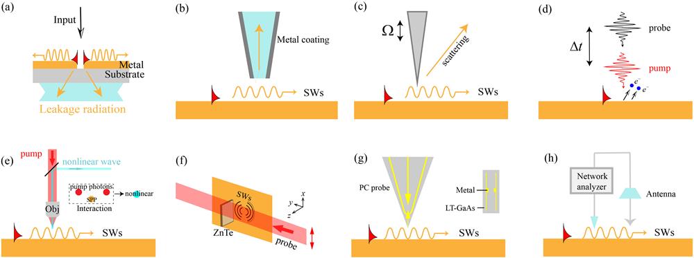
Fig. 2. (a) Working principle of the LRM, where the SPs leak through the substrate and are detected in the far field. (b) Schematic of the a-SNOM, and the SPs are coupled into the tapered probe through the aperture. (c) Schematic of the s-SNOM. (d) The pump pulse launches SPs on the sample, and the probe pulse interferes with the propagating SPs and liberates photoelectrons in a two-photon photoemission process. (e) Schematic of the NNOM setup for mapping plasmonic fields. (f) Schematic diagram for imaging the THz-SPs using electro-optic crystal. (g) Schematic of the near-field photoconductive antenna probe tip. (h) Schematic of the near-field scanning technique based on the network analyzer.
Fig. 3. (a)–(c) Modes based on prisms. (d)–(f) Methods based on diffraction from near-field tip, topological defect, and grating, respectively. (g) Method based on a high-numerical-aperture microscope objective. (h) Gong et al. utilized the parallel plate waveguide to excite terahertz SPs on a thin-film coated aluminum surface. Reproduced with permission from Ref. [190], © 2009 Optical Society of America (OSA). (i) Ng et al. adopted the Otto prism configuration to excite terahertz spoof SPPs on textured metal surface. Reproduced with permission from Ref. [191], © 2013 Wiley.
Fig. 4. (a), (b) Schematics of gradient phase metasurface in the case of anomalous refraction and SP coupling, respectively. Reproduced with permission from Ref. [194], © 2018 Wiley. (c), (d) Simulated
Fig. 5. (a), (b) SEM image and the measured results of a controllable SP coupler. Reproduced with permission from Ref. [209], © 2009 American Institute of Physics (AIP). (c), (d) SEM image and unidirectional excitation performances. Reproduced with permission from Ref. [210], © 2010 AIP. (e)–(g) Simulated results and schematic side view of a set of aperiodic grooves, and corresponding experimental results. Reproduced with permission from Ref. [211], © 2011 ACS. (h), (i) Schematic side view and corresponding experimental results. Reproduced with permission from Ref. [215], © 2014 AIP. (j), (k) Schematic view of a double-slit structure illuminated by an oblique incidence, as well as the simulated and measured results under incidences of different angles. Reproduced with permission from Ref. [219], © 2011 AIP. (l), (m) Schematic view of a long slit illuminated by oblique circular polarization and corresponding experimental results. Reproduced with permission from Ref. [144], © 2013 AAAS. (n), (o) Simulated results of a single MIM meta-atom, and the SEM image and measured SP excitations of paired meta-atoms with different separation distances. Reproduced with permission from Ref. [143], © 2012 ACS. (p)–(r) Schematics, SEM image, and measured results of a unidirectional coupler composed of paired slit resonators. Reproduced with permission from Ref. [220], © 2014 ACS. (s)–(x) Schematics and simulated results of single-slit resonators, single-split-ring-shaped slit resonators, and paired slit resonators, respectively. Reproduced from an open access reference [221].
Fig. 6. (a)–(c) Simulated field distribution of L-shaped slit resonator under the linearly (a) and circularly (b) polarized incidences, respectively; SEM images and measured results (c). Reproduced with permission from Ref. [225], © 2014 Wiley. (d), (e) SEM image and corresponding experimental results of a column of
Fig. 7. (a), (b) Schematic of experiment setup and SEM image of fabricated sample (a); measurements of SP excitations under incident linear polarization of different orientation angles (b). Reproduced with permission from Ref. [232], © 2020 Wiley. (c), (d) SEM image of a pair of coupled split-ring-shaped slit resonators (c) and experimentally obtained asymmetric SP excitations (d). Reproduced with permission from Ref. [233], © 2017 OSA. (e), (f) SEM image of a set of aperiodic slit resonators (e) and corresponding performance of on-chip wavelength multiplexing (f). Reproduced with permission from Ref. [235], © 2011 ACS. (g)–(i) Design strategy (g) and SEM image (h) of the holographic metalens; near-field measurements of wavelength-multiplexed SP excitation (i). Reproduced with permission from Ref. [236], © 2015 ACS. (j), (k) SEM image (j) and corresponding results (d) of angular-momentum nanometrology. Reproduced from an open access reference [240]. (l), (m) Schematic view (l) and simulated results (m) of spin-Hall lens design. Reproduced with permission from Ref. [241], © 2019 ACS.
Fig. 8. (a), (b) SEM image of Archimedes’ spiral-shaped grooves (a) and corresponding results under incidences of LCP and RCP (b). Reproduced with permission from Ref. [148], © 2008 American Physical Society (APS). (c), (d) Schematics and SEM image of cosine-Gauss beam launcher (c) and experimentally obtained near-field distribution (d). Reproduced with permission from Ref. [245], © 2012 APS. (e), (f) SEM image (e) and corresponding near-field results (f) of a segmental slit structure. Reproduced from an open access reference [249]. (g)–(i) Schematic of experiment setup and SEM image of fabricated slit ring (g); simulation and measurement results of different SP profiles (h); simulation results for different wavelengths (i). Reproduced from an open access reference [250]. (j) SEM image and near-field results of a plasmonic metalens composed of asymmetric ridges. Reproduced with permission from Ref. [251], © 2011 ACS. (k) SEM image and experimentally measured results from a plasmonic phase mask. Reproduced with permission from Ref. [252], © 2014 APS. (l), (m) SEM image and corresponding SP excitations from plasmonic masks with complete amplitude and phase control. Reproduced with permission from Ref. [254], © 2014 OSA.
Fig. 9. (a), (f), (n), (t) Schematics of a single-slit resonator, a pair of slit resonators, two pairs of slit resonators, and a row of slit resonators, respectively. (b), (c) Simulated SP excitation of a single-slit resonator (b); SEM images and corresponding experimental results of samples composed of slit resonators (c). Reproduced with permission from Ref. [256], © 2017 APS. (d), (e) Schematic (d) and experimentally obtained SP excitations (e) from a column of slit resonators. (g), (h) Schematic views of design strategy and corresponding results of spin-controlled SP Fresnel zone metalens and combined SP Fresnel zone metalens. Reproduced with permission from Ref. [259], © 2015 OSA. (j), (i) Schematic view (j) and corresponding results (i) of a spin-controlled SP metalens composed of paired slit resonators. Reproduced with permission from Ref. [262], © 2015 ACS. (k) Microscopy image and corresponding experimental results of SP devices composed of paired slit resonators. Reproduced with permission from Ref. [264], © 2015 Wiley. (l), (o), (p) Calculation, simulation, and experimental results of special SP profiles, respectively. Reproduced with permission from Ref. [267], © 2017 Wiley. (m) Polarization-independent SP Airy beam launching. Reproduced with permission from Ref. [268], © 2020 Wiley. (q)–(s) Schematic view and results of spin-multiplexed launching of plasmonic vortices. Reproduced with permission from Ref. [269], © 2022 Wiley. (u), (v) Phase distributions for LCP and RCP incidences, and microscopy image of fabricated sample (u); simulated and measured SP field distributions under different incidences (v). Reproduced from an open access reference [205]. (w), (x) Schematics and SEM image of the SP launcher (w); numerical and experimental results under LCP and RCP (x). Reproduced from an open access reference [272].
Fig. 10. (a) Schematic of plasmonic vortex. (b) Schematic of spiral grooves on a metal film that generates a plasmonic vortex impinged by circularly polarized light. Reproduced with permission from Ref. [285], © 2006 OSA. (c) Diagram of an Archimedes spiral structure and a spiral plasmonic lens under circularly polarized illumination. Reproduced with permission from Refs. [149,287], © 2009 OSA and © 2010 ACS, respectively. (d) Scanning electron microscope image of the segmented Archimedes spiral-shaped long-slit-based plasmonic vortex lens and experimental near-field intensity distribution of excited plasmonic vortices. Reproduced with permission from Ref. [150], © 2010 ACS. (e) Schematic of control plasmonic vortex by spiral distribution structures of multi-row slits. Reproduced with permission from Ref. [184], © 2018 Wiley. (f) Schematic of control plasmonic vortex by spiral distribution structures of single-row slits. Reproduced with permission from Ref. [260], © 2019 Wiley.
Fig. 11. (a) Researches on the spatiotemporal dynamics of plasmonic vortices. Top panels: schematic experimental methodology by time-resolved two-photon photoemission electron microscopy; middle panels: spin–orbit mixing of light with plasmonic vortices; bottom panels: experimental results within a plasmonic vortex cavity, showing the revolution stages of orbital angular momentum multiplication. Reproduced with permission from Refs. [167– 169" target="_self" style="display: inline;">– 169], © 2017 AAAS, © 2019 APS, and © 2021 AAAS, respectively. (b) Schematic of the temporal evolution progress of plasmonic vortices with the same topological charge generated by different couplers. Reproduced from an open access reference [299]. (c) Schematic of deuterogenic plasmonic vortex in the center of generated plasmonic vortex with higher topological charge. Reproduced with permission from Ref. [300], © 2020 ACS. (d) Schematic of scanning transmission electron microscope image and cathodoluminescence analysis of plasmonic vortices. Reproduced from an open access reference [301].
Fig. 12. (a) SEM image and corresponding measurements of an SP mirror composed of silver particles. Reproduced with permission from Ref. [310], © 2002 AIP. (b), (c) SEM image (b) and corresponding experimental results (c) of an SP Fresnel zone plate. Reproduced with permission from Ref. [311], © 2007 AIP. (d) Photograph and corresponding near-field characterizations of anomalous reflection phenomena. Reproduced with permission from Ref. [312], © 2018 APS. (e), (f) SEM image (e) and corresponding SP field distribution (f) of a plasmonic Airy beam launcher. Reproduced with permission from Ref. [313], © 2011 APS. (g), (h) Design strategy and corresponding experimental results of on-chip multiplexing and demultiplexing. Reproduced with permission from Ref. [314], © 2011 ACS. (i), (j) SEM image (i) and corresponding results (j) of an indefinite plasmonic beam launcher. Reproduced from an open access reference [316]. (k), (l) Schematic and simulation results of a metallic ridge (k); simulated propagating behaviors on the metasurface for SPs of different wavelengths (l). Reproduced with permission from Ref. [323], © 2013 AIP. (m), (n) Schematic and simulation results of magnetic hyperbolic metasurface (m); experimentally obtained propagating behaviors (n). Reproduced from an open access reference [122].
Fig. 13. (a), (b) Schematic and simulation results of a transformational plasmonic Luneburg lens. Reproduced with permission from Ref. [331], © 2010 ACS. (c)–(e) SEM images, simulation, and experimental results of a spoof SPP telescope (c), spoof SPP coupler (d), and spoof SPP multiplexer (e). Reproduced with permission from Ref. [336], © 2020 ACS. (f)–(h) Design strategy of complete amplitude and phase control of SP wavefront (f), and proof-of-concept experiments phase-only control (g) and amplitude-phase control (h). Reproduced with permission from Ref. [337], © 2017 ACS.
Fig. 14. (a), (b) SEM image (a) and corresponding decoupling results (b) at the propagating plane. Reproduced with permission from Ref. [339], © 2013 OSA. (c)–(e) Schematic and SEM image of directional color filter (c); calculated (solid lines) and simulated (dashed lines) relative transmission (d); and experimentally measured relative transmission (e). Reproduced from an open access reference [340]. (f), (g) SEM images and experimental results of directional SP decoupler. Reproduced with permission from Ref. [220], © 2014 ACS. (h), (i) SEM images and experimentally obtained field intensity and polarization distributions. Reproduced with permission from Ref. [341], © 2018 ACS. (j), (k) Schematics and SEM image of spin-coded meta-aperture (j); simulated and measured transmission under LCP and RCP incidences (k). Reproduced from an open access reference [342]. (l), (m) Schematics and microscopy image of spin-coded meta-hole (l); simulated and measured transmission under LCP and RCP incidences (m). Reproduced with permission from Ref. [343], © 2018 Wiley. (n)–(p) Schematic (n) and SEM image (p) of the polarization generator and corresponding experimental results (p). Reproduced from an open access reference [344]. (q), (r) SEM image (q) and corresponding experimental results (r) of multiplexed holography. Reproduced with permission from Ref. [345], © 2017 ACS. (s), (t) Schematics (s) and experimental results (t) of an SP decoupler based on gradient phase metasurface. Reproduced with permission from Ref. [346], © 2015 AIP. (u)–(w) Design strategy and phase distributions of a focusing decoupler (u); microscopy image and experimental results of the focusing decoupler (v); phase distributions and experimental results of different functional decouplers (w). Reproduced from an open access reference [348].
Fig. 15. (a)–(d) SEM images of different logic gates (a); SEM images, experimental results, simulation results of XNOR gate (b), XOR gate (c), and OR gate (d). Reproduced with permission from Ref. [351], © 2012 ACS. (e), (f) Schematic view (e) and experimental results (f) of an orbital-angular-momentum-controlled hybrid nanowire circuit. Reproduced with permission from Ref. [359], © 2021 ACS. (g), (h) Schematic view (g) and experimental results of a controllable directional SP coupler. Reproduced from an open access reference [360]. (i)–(k) Schematic view of a plasmonic tweezer (i); comparison between the plasmonic tweezer and optical tweezer (j); patterns of the letter “N” constructed by gold particles in focused plasmonic tweezers (k). Reproduced from an open access reference [363]. (l), (m) Schematic of experimental setup (l) and corresponding manipulation results (m) of a holographic plasmonic tweezer. Reproduced with permission from Ref. [364], © 2017 ACS.
Fig. 16. (a)–(d) Schematic and SEM image of the metasurface polarimeter (a), (b); simulated scattering patterns under the incidence of different polarizations (c);

Set citation alerts for the article
Please enter your email address
© Copyright 2018-2021 | Chinese Laser Press. All Rights Reserved 沪ICP备15018463号-20