1Center for Terahertz Waves and College of Precision Instrument and Optoelectronics Engineering, Key Laboratory of Optoelectronic Information Technology (Ministry of Education), Tianjin University, Tianjin, China
2Guangxi Key Laboratory of Optoelectronic Information Processing, Guilin University of Electronic Technology, Guilin, China
3School of Electrical and Computer Engineering, Oklahoma State University, Stillwater, USA
Surface plasmons (SPs) are electromagnetic surface waves that propagate at the interface between a conductor and a dielectric. Due to their unique ability to concentrate light on two-dimensional platforms and produce very high local-field intensity, SPs have rapidly fueled a variety of fundamental advances and practical applications. In parallel, the development of metamaterials and metasurfaces has rapidly revolutionized the design concepts of traditional optical devices, fostering the exciting field of meta-optics. This review focuses on recent progress of meta-optics inspired SP devices, which are implemented by the careful design of subwavelength structures and the arrangement of their spatial distributions. Devices of general interest, including coupling devices, on-chip tailoring devices, and decoupling devices, as well as nascent SP applications empowered by sophisticated usage of meta-optics, are introduced and discussed.
Free-space light can be coupled into propagating surface waves at the interface between a conductor and a dielectric (usually metal–air interface), known as surface plasmons (SPs)[1–7]. Essentially, SPs are light waves that are confined in the surface because of their interaction with the free electrons in the conductor. More specifically, the free electrons near the surface of the conductor respond collectively by oscillating in resonance with the electromagnetic field of light. Such collective oscillation creates the SP and results in unique properties called SP polaritons (SPPs) to reflect its hybrid nature. The most appealing feature of SPs is the capability to concentrate light on a two-dimensional platform and produce very high local-field intensity, providing a vital route to construct on-chip optical devices/systems and manipulate light–matter interactions[8–16]. Since the late 20th century, we have witnessed a boom in SP-related research, contributed by scientists from various fields, including physics, chemistry, materials science, and biology.
There are two main types of SPs with respect to their propagation characteristics along the interface: propagating SPs on a smooth conductor–dielectric interface and localized SPs in bound geometries such as metallic particles[1,2]. Propagating SPs are considered more classical since they have been known for a longer time. In contrast, localized SPs have recently attracted increased attention, since the advancements in micro/nano-technology have made the fabrication of subwavelength structures feasible. With carefully designed metallic structures to achieve specific field distribution and extreme field enhancement, localized SPs have rapidly boosted the development of nonlinear optics[17–21], surface-enhanced Raman spectroscopy[22–24], biochemical sensors[25–28], and so forth[29,30]. In particular, through constructing the resonance of localized SPs, the interaction between subwavelength metallic structures and incident light can be custom defined, which opens an avenue toward the flourishing field of metamaterials[31–38] (artificial materials with designable electromagnetic properties). A variety of novel physical phenomena that can hardly be achieved by natural materials have been implemented by metamaterials, such as negative refraction[31,39–43], transformation optics[44–46], transversely spinning light[47,48], and topological photonics[49–52]. In addition, two-dimensional metamaterials composed of a planar and ultrathin array of artificial structures, i.e., metasurfaces, have shown unprecedented capabilities of manipulating electromagnetic waves at will[53–69]. In free space, practical devices of general interest, such as metalenses[70–75], perfect absorbers[76–78], polarization wave plates[79–85], special beam launchers[86–89], and holograms[90–97], have been successfully demonstrated.
Parallel to the flourishing of metamaterials and metasurfaces in free space, the development of meta-optics has also brought renewed interest to the manipulation of SPs. As a promising on-chip information carrier, SPs are very attractive in developing ultracompact integrated plasmonic systems in which light and electric signals can be transferred and processed simultaneously. To build such systems, one requires a variety of components, including but not limited to: couplers to couple specific free-space light into SPs; waveguides, lenses, and splitters to manipulate the on-chip propagation behaviors of SPs; switches, multiplexers, and logic gates to perform on-chip information processing; scatterers and decouplers to link SPs with free-space information channels. However, traditional devices for coupling or manipulating SPs are either bulky or inflexible (e.g., prisms[98,99] and gratings[100]), hindering the overall compactness and possible functionalities of related SP applications. Intriguingly, the advancement of meta-optics provides a powerful solution to solve these issues. The main idea of meta-optics is constructing subwavelength artificial structures to support specific resonances or modes, including localized SP resonance on metallic structure, Mie resonance in dielectric structure, Fabary–Pérot resonance in multiple-layer structure, and propagation mode in dielectric or metallic waveguides. Through these resonances or modes, the effective optical parameters including permittivity, permeability, and chirality can be flexibly tailored by three-dimensional bulk metamaterials[31–38]; on the other hand, the local scattering responses including phase, amplitude, and polarization can be arbitrarily tailored by two-dimensional flat metasurfaces[53–69]. The underlying physics of meta-optics can also be applied to develop SP devices. In the last two decades, different kinds of SP devices have been successfully achieved with ultracompact size and superior performance through the design of suitable subwavelength structures and the sophisticated arrangement of their spatial distributions, which rapidly promoted the development of SP-related science and technology.
Sign up for Photonics Insights TOC. Get the latest issue of Photonics Insights delivered right to you!Sign up now
In this review, we discuss recent progress on meta-optics inspired SP devices. These devices can be roughly classified as four types according to their functionalities: (1) SP devices to couple free-space light to SPs, including efficient coupling, unidirectional and asymmetric coupling, polarization, wavelength, and/or orbital angular momentum multiplexed coupling; (2) SP devices to tailor on-chip propagation of SPs, including focusing, special beam launching, plasmonic vortices, and demultiplexing/multiplexing; (3) SP devices to scatter SPs to the far field, including directional scattering, polarization and/or wavelength multiplexed scattering, and special near-field distribution generation; (4) SP devices that make usage of specific SP field distributions and/or the process of conversion between free-space light and on-chip SPs, including plasmonic tweezers and light beam information detectors. This review is arranged as follows: in Section 2, we briefly introduce the fundamentals of SPs and meta-optics; in Section 3, we review the experimental setups for SP characterizations, from visible, infrared (IR), and terahertz (THz), to microwave frequencies; in Sections 4–6, we review SP devices for coupling, tailoring, and scattering of SPs, including both traditional and nascent methods; in Section 7, we discuss applications empowered by sophisticated usage of meta-optics; in Section 8, we present a summary and an outlook on possible future research directions.
2 Fundamentals
2.1 Basic Properties of SPs
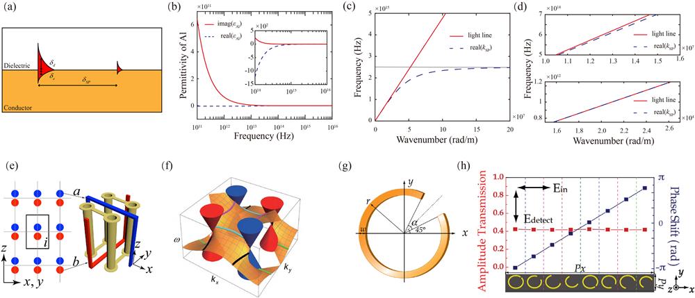
SPs can be seen as an electromagnetic wave solution of Maxwell’s equation at a given conductor–dielectric boundary [see Fig. 1(a)], whose mathematic deductions have been well studied in previous works[1,2]. We start from the dispersion relation of an SP excited at an infinite smooth conductor–dielectric interface: ɛɛɛɛwhere is the wave vector of the light of angular frequency in vacuum; is the light speed in vacuum; ɛ and ɛ are the permittivity of the dielectric and conductor, respectively. In general, ɛ and ɛ are complex quantities due to the absorption loss in the dielectric and conductor. In most cases, the conductor is metal and the dielectric is air (or vacuum, to simplify). Thus, the dispersion relation of an SP usually depends on the optical properties and dispersive properties of metals.
As a convenient fitting method, one can use the Drude model to describe the permittivity of metals: ɛɛwhere ɛ is the permittivity of metal at infinite frequency, which in general satisfies ɛ; and are the plasma frequency and scattering rate, respectively. Taking aluminum as an example, the plasma frequency and scattering rate are and , respectively. By setting as one, the permittivity of aluminum ɛ can be calculated using Eq. (2) and is given in Fig. 1(b). One can find that in the lower-frequency range, including THz and microwave frequencies, ɛ is dominated by a very large imaginary part; as the frequency increases to IR and visible frequencies, ɛ is dominated by a negative real part; as the frequency increases further, ɛ gradually converges to a fixed value. This leads to SPs having very different dispersion relations at different frequencies. Figure 1(c) shows the calculated dispersion relation of SPs at the aluminum–air interface (blue dashed line) and light line (red solid line). It can be seen that as the frequency increases, the dispersion curve separates from the light line and gradually approaches the resonance frequency of the SP, i.e., ɛ (gray solid line).
Figure 1(d) gives the zoom-in SP dispersion curve and light line at frequencies around and , respectively, corresponding to wavelengths around 300 µm and 500 nm. Obviously, around the wavelength of 500 nm (visible regime), the SP wave vector for an aluminum–air interface is larger than the free-space light wave vector. This increase in momentum is associated with binding of the SPs to the surface, and the resulting momentum mismatch of the same wavelength must be bridged if free-space light is to be used to generate SPs (discussed in detail in Section 4). In contrast, around the wavelength of 300 µm (THz regime), the SP wave vector for an aluminum–air interface is almost coincident with a free-space light wave vector (to an accuracy of one part in ), resulting in a highly delocalized homogeneous field of SPs with a large penetration depth and negligible dispersion. Actually, the appealing features of SPs including surface confinement and strong field enhancement are mainly referred to in the IR and visible ranges, and the majority of SP-related studies have been also carried out at these frequencies. Nevertheless, benefiting from the well-established semiconductor processing technology and printed circuit board technology, it is much more convenient to fabricate sophisticated samples in the THz and microwave regimes; moreover, the characterization methods at lower frequencies are capable of obtaining the full amplitude and phase information as well as exacting spatiotemporal dynamics of SP fields, which can hardly be obtained in the IR and visible ranges. Studies of SPs at THz and microwave frequencies could explore general underlying physics, which are applicable to IR and visible frequencies, but can hardly be directly investigated at these frequencies due to limitations of current technology[14,15,101–103]. Therefore, this review also covers SP devices at THz and microwave frequencies.
Once an SP mode is excited on a flat metal surface, it will propagate along the surface but gradually attenuate owing to the losses arising from absorption in the metal and dielectric. The propagation length [see Fig. 1(a)] can be found by seeking the imaginary part of the SP wave vector , which determines how long the intensity of SPs can be maintained. The propagation behavior of SPs on a smooth metal–dielectric surface follows the two-dimensional version of the Huygens–Fresnel principle[6,104]. For a relatively absorbing metal such as aluminum, the propagation length at a wavelength of 500 nm is approximately 2 µm. For a low-loss metal, such as silver, the propagation length at a wavelength of 500 nm is approximately 20 µm. In this manner, the propagation length sets the upper size limit for the SP-based circuit. In contrast to the propagating nature of SPs along the surface, the SP field normal to the surface decays exponentially with distance from the surface. The field in this direction is called the evanescent field or near field in nature, and is the result of the bound and nonradiative nature of SPs, which prevents power propagating away from the surface. The decay length in the dielectric [see Fig. 1(a)], ɛ, determines the level of confinement and dictates the maximum height of any individual devices that might be used to control SPs. On the other hand, the decay length in the conductor [see Fig. 1(a)], ɛ, determines the minimum feature size that can be used, which in the visible range is about one or two orders of magnitude smaller than the wavelength involved.
In addition to metals, other materials such as doped semiconductors, superconductors, or graphene can also support SP modes, since they are known to be good conductors (at least for direct currents). In 2003, Rivas et al. demonstrated the plasmonic behavior of extraordinary optical transmission of THz waves through periodic arrays of holes made in highly doped silicon wafers[105]. Shortly after, they further demonstrated time-domain measurements of THz SPPs propagating on gratings structured on doped silicon[106]. In 2005, Savel’ev et al. predicted the existence of THz surface waves in layered superconductors below the Josephson plasma frequency , which is the first prediction of propagating surface waves in any superconductor[107]. Since then, the theory and applications of surface Josephson plasma waves have been rapidly developed[108]. In 2010, Tsiatmas et al. demonstrated the extraordinary optical transmission effect through an array of high-temperature superconductor subwavelength holes[109]. In 2012, Vakil et al. and Koppens et al. theoretically predicted transformation optics[110] and strongly enhanced light–matter interactions[111], respectively, based on graphene plasmonics, indicating the much tighter confinement and relatively long propagation distance of graphene plasmons in comparison with metal plasmons. In addition to graphene, many other two-dimensional materials have also been intensively investigated, whose plasmonic properties are exciting and often different from the properties of their three-dimensional parent materials[112]. Inspired by these pioneering works[105–112], enormous endeavors have been made in exploring the new physics and nascent applications of plasmonics in different material systems, and novel devices working in different frequency ranges with excellent performances have been successfully achieved. Further details on the basic mechanisms and potential applications of plasmonics in different materials as well as their hybrid-material systems can be found in various reviews[15,112–114].
2.2 Basic Concepts of Meta-optics
Metamaterials are engineered structures designed to interact with electromagnetic waves in a desired fashion[31–38]. They usually comprise an array of structures smaller than the wavelength of interest. These so-called meta-atoms can interact with the electric and magnetic components of electromagnetic waves in a way that natural atoms do not. Generally, metamaterials can be described by the effective medium model due to the deep subwavelength size of meta-atoms, and the constitutive relation can be expressed in the most general formula: ɛɛHere, ɛ, , , are all tensors, where ɛ and are the relative permittivity and permeability tensors, respectively; and are magneto-electronic tensors. For a Hermitian system, they satisfy ɛɛ, , . These tensors can be engineered via the judicious design of resonator configurations. Taking the work by Biao Yang et al. as a realistic example[50], here, we show how sophisticated meta-atoms can be designed to manipulate the effective medium parameters. In this work[50], Biao Yang et al. demonstrated a photonics ideal Weyl semimetal, which consists of periodically buried saddle metallic coils in substrate materials with a dielectric constant of 2.2. Further analysis of the electromagnetic response reveals that the unit cell of the saddle metallic coil can be treated as two splitting resonance rings (SRRs), which behave as two particles on each lattice, as schematically shown in Fig. 1(e). By considering the motion of electrons driven by an external homogeneous electromagnetic field on those metallic components, the driving electric potential can be written as[115]where indicates electric current, is the electric charge, is the inductance on the SRRs, , with capacitance as the resonance frequency, and and are the effective area and length of SRR, respectively. By neglecting the ohmic loss and the interaction between intra and inter layers, the effective medium tensors can be calculated as ɛ
Clearly, Eqs. (4)–(7) give a direct link between realistic meta-atom parameters and effective medium parameters. Such meta-atom composed metamaterial exhibits four Weyl points at the same energy [see Fig. 1(f)], the minimum number allowed in the presence of time-reversal symmetry. This metamaterial design offers an ideal platform for the investigation of various unconventional physics in Weyl systems[51,116,117]. A broader scope of studies on metamaterial design can be found in Refs. [31–38].
The validity of the above-discussed effective medium model requires two preconditions: overall three-dimensional bulky size and subwavelength meta-atoms. When the thickness of metamaterials shrinks to the deep subwavelength scale, i.e., turns into metasurfaces, it is not rigorous anymore to calculate the effective medium parameters. Instead, it is of more interest to control local scattering properties, such as polarization, phase, amplitude, and dispersion, of ultrathin meta-atoms after their interactions with incident light. In general, the target functionalities of metasurfaces are achieved by the collective scattering of light by all the meta-atoms[53–69]. Here, as a classic design, a C-shaped metallic resonator is chosen as an example to show how to construct functional metasurfaces[118]. As shown in Fig. 1(g), the C-shaped metallic resonator is designed to have an arcminute line of the split 45° with respect to the axis and supports various resonances. More specifically, the incident electric fields oriented along the and axes could excite different localized SP resonances along the C-shaped metallic resonators. Due to the resonance induced anisotropy, when incident with an -polarized wave, the transmitted wave would retain not only the -polarized component, but also an orthogonally polarized component along the axis. Being orthogonal to the incident wave, the direction transmission amplitude and phase shift can be significantly modulated by changing the radius and open angle of C-shaped metallic resonators. Another feature of the resonator is that the phase shift of the outgoing -polarized wave changes by when the resonator is rotated 90° or along its central axis, without any variation in the transmission amplitude. Such phase shift of can be attributed to the Pancharatnam–Berry (PB) phase concept[58,119,120], which is robust and broadband for orthogonally polarized components. By carefully designing the geometric parameters, four resonators with nearly identical transmission amplitudes and a phase increment for the -polarized wave are selected, as shown in Fig. 1(h). By simply rotating each of these resonators by 90°, another phase range can be covered. In this manner, different wavefront control devices including diffraction gratings, focusing lenses, and Fresneal zone plates can be achieved by properly arranging the kinds and locations of C-shaped metallic resonators along the surface to satisfy specific phase distributions. More importantly, the amplitude of the orthogonally polarized component can be simply controlled by changing the orientation angle of the C-shaped metallic resonators, without influencing their phase shift control[121]. Such simultaneous control of phase and amplitude empowers further complex wavefront control devices, such as multi-ordered diffraction gratings[121] and meta-holograms[96]. A broader scope of studies on metasurfaces can be found in Refs. [53–69].
Clearly, through the design of suitable meta-atoms and their spatial arrangement, meta-optics provides a brand-new solution for the manipulation of light–matter interactions. In general, under the conductor–dielectric condition, only transverse magnetic (TM, p-polarized) waves can excite SPs, and excited SPs also exist as TM modes along the surface. Benefiting from the high design flexibility of meta-optics, one can design proper metacouplers to convert transverse electric (TE, s-polarized) waves into SPs; more intriguingly, beyond the traditional TM mode SP, one can construct proper metasurfaces to support the propagation of generalized surface waves as eigen modes on them, such as TE mode surface waves[122–124], spoof SPPs[125–130], Bloch surface waves[131–135], and topological surface states[49,136–141].
3 Characterizing Technologies
In the last decades, the study of near-field optics and photonics has gained increasing enthusiasm, and the ability to form images underlies many advances in both science and technology. The early detection methods for SP waves were often indirect, where one had to convert the near-field wave to free-space propagating waves for characterization. Although the principle of these methods is simple, the operation is complicated, and it is difficult to obtain high spatial resolution. To further increase the ability of direct detection, many near-field methods for SP characterization have been proposed.
3.1 Visible and Infrared
Leakage radiation microscopy. Leakage radiation microscopy (LRM) can be an alternative way to probe near-field waves, and a typical setup of LRM is presented in Fig. 2(a). The leakage radiation through the substrate is further detected in the far field. As a versatile method for direct imaging of SPs, LRM is a powerful tool allowing quantitative analysis, in both direct and Fourier momentum spaces, which has already been successfully applied to analyze the efficiency of directional excitation of SPs[142,143]. Shortly after, based on the LRM, Francisco et al. described vectorial near-field interference using a simple circularly or elliptically polarized dipole to achieve directional broadband excitation of guided modes[144]. In 2016, Jiang et al. experimentally demonstrated spin-dependent directional coupling as well as vortex generation of SPs by nanostructures[145]. It realized the implementation of LRM to probe the chirality of plasmonic structures, and quantitative inspections, including directivity and extinction ratio measurements, were achieved via polarization analysis in both image and Fourier planes. Subsequently, Sinev et al. visualized the directivity patterns of SPs excited on a thin gold film by a single silicon nanosphere using an LRM setup combined with Fourier plane imaging optics[146]. They pointed out that a high-index dielectric nanosphere could also achieve the directional coupling of light to surface waves even using a linearly polarized pump beam. Despite the fact that the LRM provides a simple and reliable way to characterize SPs, current LRM can be applied only to plasmonic structures with transparent substrates, and it cannot provide phase information.
Figure 2.(a) Working principle of the LRM, where the SPs leak through the substrate and are detected in the far field. (b) Schematic of the a-SNOM, and the SPs are coupled into the tapered probe through the aperture. (c) Schematic of the s-SNOM. (d) The pump pulse launches SPs on the sample, and the probe pulse interferes with the propagating SPs and liberates photoelectrons in a two-photon photoemission process. (e) Schematic of the NNOM setup for mapping plasmonic fields. (f) Schematic diagram for imaging the THz-SPs using electro-optic crystal. (g) Schematic of the near-field photoconductive antenna probe tip. (h) Schematic of the near-field scanning technique based on the network analyzer.
Aperture-type SNOM. To detect the surface wave with subwavelength spatial resolution, scanning near-field optical microscopy (SNOM) has been employed. Since 1998, when Hunsche et al. introduced a metallic aperture into the characterization system[147], near-field imaging based on a subwavelength aperture (a-SNOM) has been rapidly developed. A schematic of the a-SNOM is illustrated in Fig. 2(b). The SP fields are detected by the tapered metal-coated (Cr/Au) probe tip with a nanometer-level aperture. Early implementation of the a-SNOM to characterize surface waves in the visible regime can be traced back to works published by Hasman’s group in 2008[148], where the field distribution of plasmonic vortices generated by spiral grating is measured. Together with the simulated phase distributions, they unveil the spin-dependent nature of plasmonic vortices in nanoscale structures. Later, it was experimentally confirmed that plasmonic vortices can be generated by a single Archimedean spiral structure, and the SP intensity distribution was directly imaged by a collection mode a-SNOM using a tapered fiber probe with a nominal aperture size of 50–80 nm[149]. Kim et. al numerically and experimentally verified the feasibility of generating plasmonic vortices with arbitrary higher-order topological charges by illuminating with a circularly polarized light (), and the number of topological charges can be extracted by calculating the size of primary rings in the intensity distributions[150]. In 2014, Klein et al. studied the polarization characteristics of light emission and collection in the near field by the tips of a dual-SNOM (two-SNOM) setup[151], which realized the first direct near-field measurements of dipole-like SP emission from aperture SNOM tips. Although a-SNOM can map the surface wave intensity distribution with subwavelength resolution, the phase distribution cannot be obtained. In addition, due to the cylindrical symmetry of tapered fiber probes, they are more sensitive to in-plane electric field components and . However, for SPs, the electric components perpendicular to the surface are of more interest, which limits the application of a-SNOM.
Scattering-type SNOM. It is well known that metallic edges or sharp extremities can scatter off light incident on it, which can serve as an alternative detection technique—scattering-type SNOM (s-SNOM)[152]. As shown in Fig. 2(c), the near-field interaction between the tip and sample modifies the tip-scattered field depending on the local dielectric properties of the sample. Both amplitude and phase information of the surface wave can be simultaneously recorded due to pseudo-heterodyne interferometric detection[153]. Therefore, the s-SNOM can be employed for both imaging[154] and spectroscopy[155] with subwavelength resolution. In practice, resolution is typically determined by the size of the tapered tip, independent of the wavelength of the illumination source. An atomic-force-microscope (AFM) tip is often used as a base instrument to realize the detection. To suppress the background signal scattered from the tip, Ocelic et al. proposed the higher-harmonics demodulation method, capable of background interference elimination in the entire near-UV to far-IR spectral range[153]. In 2018, Ostrovsky et al. presented nanoscale spatial control over optical singularities on a metal–air interface by varying the polarization state of the light exciting SPs through a spiral slit[156]. The full-field distribution was mapped by phase-resolved s-SNOM showing both amplitude and phase at 15 nm resolution.
Scanning tunneling microscopy. Another powerful technique to investigate SPs propagating at the interface with subwavelength resolution is the scanning tunneling microscope (STM), also used in the THz region[157], where a sharp tip is placed in the immediate vicinity of the sample surface using an appropriate feedback-loop technique. Through measuring the current caused by electron tunneling between the surface and the metal tip, the near-field information of surface waves can be characterized. Liu et al. combined the STM with local optical excitation and detection to examine the near-field properties at nanometer scale[158]. Moreover, the photon STM (PSTM)[159], which collects photons by coupling the evanescent near field to propagating modes inside a tapered optical fiber, adds new information to STM. Weeber et al. used the PSTM to perform near-field observations of SP modes, excited at a visible frequency, on a metal stripe[160].
Photoemission electron microscopy. Time-resolved measurement is also of great importance to extract the dynamical information of SPs. Kubo et al. reported a hybrid technique, interferometric time-resolved photoemission electron microscopy (ITR-PEEM)[161,162], which combines the time resolution of femtosecond laser spectroscopy with the sub-optical wavelength imaging of photoelectrons. A schematic of the PEEM is illustrated in Fig. 2(d). By scanning the mutual delay between identical, phase-correlated pump and probe pulses and recording the resulting changes in a polarization interference pattern, one can create time-resolved PEEM movies with 50 nm spatial resolution to study the coherent dynamics[112] and packet evolution[113] of surface waves. Compared with electron probe methods, ITR-PEEM takes a more pragmatic approach to performing ultrafast microscopy by separating the roles of electrons and photons in achieving space and time resolution: time resolution is entirely achieved by employing the time structure of ultrafast laser pulses that excite nonlinear multiphoton photoelectron emission from the sample, while space resolution is achieved by imaging the photoelectron spatial distribution with electron optics[163,164]. This design enables lots of meaningful investigations of SPs[115], such as the two-dimensional reconstruction of the plasmonic field in space and time[165], the dynamics of plasmonic skyrmion[166] and vortices[167,168], light spin and plasmon orbit mixing[169], and the emerging field of topological plasmonics[170–172].
Other types. Nonlinear optics also shows great promise for highly tunable, non-perturbative and real-time imaging of surface waves. As shown in Fig. 2(e), Frischwasser et al. introduced nonlinear near-field optical microscopy (NNOM) to map two-dimensional evanescent plasmonic patterns through transforming both the spatial and temporal information stored in the near-field wave into nonlinearly generated propagating waves that can be collected by conventional optics in free space[173]. Alternatively, the time-resolved photon-induced near-field electron microscopy (PINEM) technique[174] has recently demonstrated additional control of SP properties, as well as the possibility to film their evolution with femtosecond-level resolution. Based on this technique, Piazza realized simultaneous observation of the quantization and interference pattern of near-field plasmons[175], which allows the observation of surface waves in multiple dimensions—space, time, and energy—yielding unprecedented insight into their fundamental properties.
3.2 Terahertz and Microwaves
Some of the characterizing methods mentioned above are also applicable to the THz and microwaves regions. Wang et al. proposed THz near-field microscopy based on an air–plasma dynamic aperture, where two mutually perpendicular air–plasmas overlap and form a cross-filament to modulate the incident THz beam without approaching the sample with any physical devices[176]. There are also other methods applied to realize near-field measurement in the THz and microwave regions.
Electro-optic crystal. One typical method to characterize SPs in the THz region is to utilize electro-optic sampling on the basis of the traditional THz time-domain spectroscopy setup. ZnTe crystal is commonly used as the detection medium, and the time-domain propagation properties of the coupled THz electric field can be measured at any point by simply moving the detection crystal and the optical probe beam. Compared with the conventional SNOM probes, such as metallized tapered fibers with a subwavelength aperture at the apex, which are typically sensitive to the in-plane component of the electric field, and the apertureless s-SNOM probes, sensitive to the out-of-plane component, the electro-optic sampling system can realize complete three-dimensional scanning of the surface wave. Based on this configuration, Zhu et al. characterized independently the vector components of the propagating plasmonic field[177]. Gacemi et al. used ZnTe to study the dispersion relation and confinement of THz SP modes[178]. Wang et al. designed an expanded line probe femtosecond beam generated by using an inverse telescope system and a slit[179,180]. As shown in Fig. 2(f), illuminating this beam onto the ZnTe detector, the THz SP field distribution can be directly captured without a two-dimensional raster scan, which greatly improves the detection speed. Nevertheless, the above system still needs a one-dimensional raster scan. In 2015, Wang et al. designed a THz digital holographic imaging system to characterize the temporal evolution of THz surface waves. In this system, the movement between the sample and the ZnTe detector was thoroughly avoided to outstandingly reduce the experimental time and strengthen the measurement stability[181].
Photoconductive antenna. A promising SNOM alternative for near-field characterizing in the THz region is based on a miniaturized photoconductive antenna probe (PC-SNOM). As shown in Fig. 2(g), through designing the antenna gap, the triangular-shaped probe with low-temperature grown GaAs switches can be used to interact with THz SP waves vertically with high resolution[182]. When the gap direction is perpendicular to the sample surface, information of SP fields can be detected. Based on such a near-field probe, Xu et al. reported a near-field scanning THz microscopy system. The probe femtosecond beam was coupled into an optical fiber and then guided to the antenna probe, fixed on a two-dimensional translation stage to realize the mapping THz SP field distribution[183]. Using a commercial THz near-field probe as the detector, Zang et al. investigated arbitrary orbital angular momentum values of a THz plasmonic vortex and coherent superposition between two orbital angular momentum states, which provides great freedom to modulate THz near-field plasmonic vortices[184].
Vector network analyzer. In the microwave regime, the vector network analyzer (VNA) is often used to realize near-field characterizations on metasurfaces. In 2012, Sun et al. experimentally demonstrated that a specific gradient-index meta-surface can convert propagating waves in free space to surface waves with nearly 100% efficiency[185]. The near-field scanning technique based on VNA was adopted to map the local-field distribution with phase information included, as illustrated in Fig. 2(h). Based on the VNA system, Zhang et al. measured the reflection and transmission coefficients of a special plasmonic waveguide, which can realize efficient amplification of spoof SPP at microwave frequency[129]. Shortly after, Cui and colleagues extended the spoof SPP to vortex beam generation, which can be employed to increase the channels in wireless communications, and electric field scanning measurements were obtained based on the VNA in an anechoic chamber[186,187].
4 Coupling Devices
4.1 Traditional Devices
A key step to implement SP-related applications is converting propagating light into SPs. Traditionally, there are two main requirements to excite propagating SPs on a smooth metal surface from the light in adjacent dielectric media: (1) incident light should be p-polarized light since the SPs are TM mode; (2) the wave vector component of the incident light parallel to the surface must equal the wave vector of the SPs. The first condition can be easily satisfied, and most efforts have been made to meet the second condition. As we discussed in Section 2.1, in visible and IR ranges, the SP wave vector is larger than the magnitude of the wave vector of the light in the adjacent dielectric medium. Thus, light illuminating a metal surface through adjacent dielectric media cannot directly couple to SPs. Here, we introduce several traditional methods capable of providing the necessary wave vector conservation.
Prism. As a simple and robust method, prism coupling methods have been widely used in the field of biochemical sensing. In the Kretschmann configuration [Fig. 3(a)], a metal film is illuminated through a dielectric prism at an angle of incidence greater than the critical angle for total internal reflection[98]. Benefited by the optically denser medium of prism material, the wave vector parallel to the metal surface increases to at the angle of incidence . By carefully choosing and , in the prism can be tuned to coincide with the SP wave vector at the air–metal interface; in this manner, resonant light tunneling through the metal film occurs, and light is coupled to SPs with very high efficiency. It should be emphasized that, with the increase in metal film thickness or with the increase in wavelength to the far-IR range, the coupling efficiency of SP excitation decreases, as the light fields are more difficult to tunnel through the metal film. To excite SPs on the internal metal interface, an additional dielectric layer with a refractive index smaller than that of the prism should be deposited between the prism and the metal film [Fig. 3(b)]. In such a two-layer geometry, both SP modes on the metal–air interface and on the metal–dielectric interface can be excited at different angles of illumination. For surfaces of bulk metal, SPs can be excited in the Otto configuration [Fig. 3(c)][99]. The total internal reflection surface of a prism is placed close to the metal surface, where light can pass through the air gap between the prism and the metal surface, giving rise to SP excitation at the metal–air interface.
Diffraction. When light focuses on a tip[188] [Fig. 3(d)] near a metal surface or a topological defect[189] on the metal surface [Fig. 3(e)], it is diffracted into different directions. Since such diffraction effects occur in the near-field regime, there are components that satisfy the matching conditions required to excite SPs. This is a simple approach for excitation; however, the efficiency is typically low because only a small part of the diffracted light satisfies the matching conditions. Another coupling method using diffraction effects is constructing periodic gratings[100] [Fig. 3(f)]. The wave vector of SPs can be matched as , where is the period, and is an integer (1, 2, 3, …). Such a periodic grating provides a well-defined spatial frequency component that mixes with the incident spatial frequency so that there can be a strong component that matches the wave vector of the SP, thus improving the overall coupling efficiency. However, the periodic grating can also provide a wave vector for propagating SPs to be decoupled to the free space of the specific angle . As such, the coupling and decoupling processes simultaneously occur on the grating.
Focusing. The combination of a high-numerical-aperture microscope objective with a thin metal film can also be used to generate SPs [Fig. 3(g)]. This can be understood in that the focusing beam with a bending wavefront in a high-index microscope can provide perpendicular components and additional vectors to satisfy the matching condition, enabling SPs to be excited on the upper surface of metal film. Different from the flat wavefront of SPs excited by the two methods above, SPs excited by a microscope objective propagate toward the center and then interfere to produce a strong convergence point, which can be combined with traditional microscopic systems and thus has been widely used in biological imaging and sensing.
It should be emphasized that the above-discussed traditional coupling methods mainly consider how to match the momentum mismatch between free-space light and SPs, which is a serious issue at visible and IR frequencies. However, the wave vector of SPs at THz and microwave frequencies is almost coincident with that of free-space light, which makes it hard to distinguish between free-space waves and propagating SPs at these frequencies, as well as hard to excite a pure SP wave. To apply the above-mentioned coupling methods at THz and microwave frequencies, one needs to apply proper designs to enhance the confinement of SPs[15]. The simplest solution is coating a thin dielectric film at the metal interface, where the configuration can be seen as a grounded dielectric film waveguide that effectively acts as a dielectric slab waveguide whose thickness is doubled. In 2009, Gong et al. carried out an experimental study on the propagation behavior of THz SPs on coated aluminum surfaces and revealed the enhanced confinement of SPs[190]. In this work, they first coupled free-space waves into a parallel plate waveguide by a lens, and then guided the waveguide mode onto the thin-film coated metal surface [see Fig. 3(h)]. Another solution is constructing subwavelength periodic structures on metal surfaces to apply the spoof SPP concept[14,101,102], discussed in detail later. In 2015, Ng et al. adopted the Otto prism configuration [Fig. 3(i)] to couple THz free-space waves into spoof SPPs on a textured metal surface and further demonstrated its sensing applications[191,192].
4.2 Gradient Phase Metacouplers
The above-discussed traditional SP couplers are excessively bulky in size, making them inconvenient for integration into compact systems. In 2011, Capasso and colleagues proposed that by arranging a set of ultrathin meta-atoms as phase shifters at the interface between two media, the reradiation wavefront of incident light after interaction with these meta-atoms can be arbitrarily manipulated[193]. These kinds of metasurfaces, known as phase discontinuity or gradient phase metasurfaces, are the major branch of metasurface studies and have attracted great attention in the last decade due to their compact physical size and unconventional optical functionalities[53–67]. Considering a spatial distribution of gradient phase shifters at the interface between two media [see Fig. 4(a)][194], refraction can be expressed by the following generalized formula: where and are the refractive indices of input and output media, respectively; and are angles of incident and transmitted light, respectively, with respect to the normal direction of the interface; is the phase gradient along direction. In the case of normal incidence ( is equal to zero), is fully dependent on and . Based on Huygens’s principle, this phenomenon can be understood by considering each meta-atom as a source of secondary wavelets that spread out in the forward direction. As schematically shown in Fig. 4(a), the transmitted light at the air side () exhibits anomalous refraction with . As the wavefront bends with angle , the refraction is actually constituted by both and components. Clearly, the component increases as increases. In the specific case where the phase gradient equals the SP wave vector, , as schematically illustrated in Fig. 4(b). In this case, the refraction waves are bent to propagate along the surface, where almost all the refraction electric fields exist as components, and thereby are coupled to SPs. As a realistic instance, Figs. 4(c) and 4(d) illustrate the simulation results of both conditions.
As discussed above, by arranging proper meta-atoms to satisfy the phase gradient , an SP coupler with ultrathin thickness can thus be achieved. Such a paradigm was first proposed by Zhou and colleagues in 2012[185]. As shown in Fig. 4(e), they utilized metal-insulator-metal (MIM) meta-atoms to construct the metacoupler for microwaves, where the desired phase gradient along the direction is achieved by varying the geometric parameters of the upper layer H-shaped metallic resonators. In this manner, the incident free-space waves can be converted to TM mode surface waves with nearly 100% efficiency. Figure 4(f) shows the measured and simulated distributions, which verifies that a metasurface of gradient phase can couple normal incidence into TM mode surface waves. It should be emphasized that, since the metasurface is spatially inhomogeneous, it cannot support TM mode surface waves as an eigen mode propagating on it[195]. The converted surface waves are known as driven surface waves. To guide the driven surface waves out, they placed a properly designed mushroom metasurface at the propagation end of a metacoupler, which can support eigen TM mode surface waves[185]. Shortly after, Bozhevolnyi et al. extended this concept to the communication band () to realize an SP coupler by an MIM metasurface [see Fig. 4(g)][196]. In addition to introducing a phase gradient in one direction, this work introduces another phase gradient in the vertical direction, which can achieve polarization selected SP coupling by horizontal or vertical polarization [see Figs. 4(h) and 4(i)]. In 2018, Ding et al. extended this concept into the visible range and further developed the design to achieve bifunctionality, that is, allowing for simultaneous polarization-controlled unidirectional SP coupling and beam steering at normal incidence[197]. The designed bifunctional metasurfaces, consisting of anisotropic MIM resonator arrays, produce two different phase gradients along the same direction for respective linear polarizations of incident light, resulting in distinctly different functionalities realized by the same metasurfaces. Ding et al. experimentally demonstrated unidirectional SP excitation within the wavelength range of 600–650 nm and broadband (580–700 nm) beam steering (30.6°–37.9°) under - and -polarized incidences, respectively.
Different from traditional methods limited to p-polarized incidence, gradient phase metacouplers can also be designed for s-polarized incidence. This can be achieved by adopting meta-atoms that acquire the desired phase shift from an orthogonal linear polarization conversion process. For instance, Liu et al. adopted anisotropic MIM meta-atoms to construct a metacoupler at the THz frequency, where the upper resonator is a square split ring with an open angle along the diagonal direction [see right-bottom plane of Fig. 4(j)][198]. Such kind of meta-atoms could efficiently convert incident polarization to polarization in reflection, and vice versa, and the phase response can be arbitrarily manipulated by changing geometric parameters of split ring resonators. By constructing phase gradient by such meta-atoms, -polarized incident free-space light can be converted into TM mode driven surface waves along the direction. Once a planar structure that supports an eigen SP mode is placed at the end of a metacoupler, the driven surface waves can be guided out as SP modes, similar to that of Ref. [185]. In this configuration, the TM surface waves are excited by s-polarized incidence, which is distinct from that of traditional methods. More interestingly, when the incidence turns into polarization, the same metacoupler can convert the incidence into TE mode driven surface waves. To illustrate the dual mode excitations, Liu et al. placed a quartz wafer in the end of a metacoupler [see Fig. 4(j)], which can support the propagation of both TM and TE modes. In this work, - and -polarized incidences share the same phase response along the same direction; as such, the corresponding excited driven surface waves propagate along the same direction but exist as different modes. Shortly after, Liu et al. extended this design to the microwave frequency and further developed the metacoupler design[199]. In this work, basic meta-atoms are also MIM-type resonators, but the upper layer structures are replaced by oval metal resonators, which respond differently than - and -polarized incidences. By carefully arranging the geometric parameters of oval metal resonators [see Fig. 4(k)], the metacoupler has two phase gradients along and directions, respectively, under - and -polarized incidences. Due to the mirror symmetry of oval metal resonators, there is no orthogonal linear polarization conversion occurring. In this manner, polarization-controlled TE mode surface waves can be excited by different incidences, as shown by Figs. 4(l) and 4(m). It should be emphasized that by flipping the phase gradient for - and -polarized incidences or changing the phase gradient for anomalous refraction, polarization-controlled TM mode surface wave coupling and beam steering can be achieved, similar to that of Refs. [196,197].
In the above-mentioned metacouplers, the required phase responses are all achieved by changing the meta-atom geometric parameters to an altering dynamic resonance phase. Alternatively, one can utilize the PB phase that occurs in the orthogonal polarization conversion process of circularly polarized light, which is also known as geometric phase. More specifically, by properly designing a meta-atom capable of converting incident left- or right-handed circular polarization (LCP or RCP) to orthogonal polarizations, the converted RCP or LCP will acquire an additional phase dependent on the orientation angle of the meta-atom. In general, any anisotropic meta-atoms can produce orthogonal polarization conversion. The most used meta-atoms are C1 or C2 rotational symmetric, whose PB phase response is with , representing the spin direction of incident circular polarization[119,200]. One recent work demonstrates that high-order PB phases equal to multiple times the orientation angle could be achieved by meta-atoms with high-fold rotational symmetries[148]; however, the main limit of high-order PB phases is the relatively low polarization conversion efficiency. The first work to apply a PB phase to construct an SP metacoupler was proposed by Prof. Zhang and colleagues in 2013[201]. The basic meta-atom is a slit resonator milled in metal film, as shown in Fig. 4(n). By spatially rotating the slit resonators to get the desired phase gradient , with the period between adjacent slits, spin-dependent SP coupling can thus be achieved. As shown in Fig. 4(o), the coupled SPs propagate toward and directions depending on the spin direction of incident circular polarization. It should be emphasized that the slit resonator is a kind of single-layer metallic resonator, which has a theoretical limitation of 25% of cross-polarization conversion[202,203]. In addition, surface waves coupled by PB phase metacouplers contain both TM and TE components, while only the TM component can be supported for propagation in the metallic–dielectric interface and then be coupled as SPs. Therefore, these conditions limit the SP coupling efficiency of single-layer metallic PB meta-atoms to below 12.5%. To improve the coupling efficiency, one can adopt MIM-type[124,143,185] or multiple-layered[204] PB meta-atoms as basic elements, which can theoretically have 100% efficiency in PB phase control and approach 50% efficiency in SP coupling (due to the mode mismatch of TE components). Nevertheless, a recent work indicates that the MIM-type PB metacoupler could achieve coupling efficiency over 50%, which can be attributed to mode conversion from the TE component to the SP mode[205]. On the other hand, to overcome the mode mismatch problem and further improve overall coupling efficiency, one can construct a proper metasurface that simultaneously supports the propagation of both TM and TE components with the same wave vector [see Figs. 4(p) and 4(q)][124].
One may notice that the above-mentioned gradient phase metacouplers are mainly achieved by reflection-type MIM metasurfaces. In general, an MIM meta-atom consists of a metallic subwavelength resonator and a continuous metal film separated by a dielectric spacer. Due to the existence of a metallic ground plane, there are only two possible channels for incident electromagnetic waves, i.e., absorption and reflection. By adopting proper constituent materials to reduce absorption loss, one can obtain very high efficiency in the reflection channel[206,207]. Then, by appropriately tuning the geometrical parameters and spatial arrangements of a set of MIM meta-atoms, this kind of metasurface can easily achieve high efficiency in converting incident free-space light into driven surface waves. However, if taking insight into SP couplers, one can find that the most important metric is actually the feed-out SPs that could be utilized for the target system. Despite the fact that MIM-type metacouplers can lead to high conversion efficiency, they also suffer from significant scattering loss when the generated driven surface waves propagate along the metasurface[195]. In contrast, though single-metallic-resonance-layer metasurfaces have relatively lower conversion efficiency, their main body is a metal film that can more favorably support the propagating surface waves, which renders scattering loss lower. To quantitatively analyze the excitation performances, Xu et al. performed simulation studies of different kinds of metacouplers, including C-shaped slit resonators, PB-phase-based slit array, MIM-type reflectarray, and also single-slit resonators [corresponding schematics are illustrated in Fig. 4(r)][194]. Figure 4(s) illustrates the simulated -field-amplitude as a function of the number of super units for each metacoupler; in each super unit, the phase gradient covers the range over a distance of . Obviously, the SP excitation of single-slit resonators is much less than that of the others, which can be attributed to a small duty cycle. For C-shaped slit resonators and PB-phase-based slit arrays, they have a comparable duty cycle and share the same efficiency limitation in converting free-space light into driven surface waves; nevertheless, the SP excitation of the former is higher than that of the latter. This is because the excitation from the PB-phase-based array contains both TM and TE components, while only the TM-polarized component can be supported for propagation, and therefore, such a mode mismatch reduces SP excitation. In the case of an MIM-type reflectarray, SP excitation is initially much larger than those of the other couplers. However, it becomes saturated as increases due to the large scattering loss, as discussed above. In contrast, the SP excitation growth of C-shaped slit resonators decreases much slower, which causes it to exhibit higher excitation than that of the MIM-type reflectarray when . A comparison of these excitations indicates a trade-off between the conversion efficiency from free-space light into driven surface waves and the scattering loss on the surface of the metacoupler. To solve this problem, Prof. Zhou and colleagues proposed a new paradigm of metacoupler design, in which the gradient phase is provided by a transmissive multiple-layered metasurface, and the converted driven surface waves are directly guided out and propagate at an additional metasurface [see Fig. 4(t)][204]. They verified this design at the microwave frequency and experimentally obtained an extremely high efficiency of 73%.
4.3 Unidirectional and Asymmetric Coupling
For the purpose of feeding on-chip plasmonic systems, unidirectional and asymmetric couplers that couple incident free-space light into SPs toward specific on-chip directions have long been pursued. The above-discussed gradient phase metacouplers could serve as one solution of unidirectional coupling, since the coupled SPs propagate along the direction of the phase gradient. In this section, we introduce more design strategies for unidirectional and asymmetric excitation of SPs.
The first design strategy is utilizing the combination of a backside illuminated slit and a Bragg grating (periodic array of grooves). For the backside illuminated slit, SPs are excited toward both sides of the slit. By properly choosing the period of the indentations, an SP of specific wavelength emerging from the slit to the grating side can be selectively backscattered. The interference of this reflected SP with the SPs excited from the slit to the right side can be tuned by adjusting the separation between the slit and the grating. In 2007, López-Tejeira et al. first proposed this design strategy, demonstrating a strong SP beam propagating away from the slit in the direction opposite to the grating and thereby demonstrating unidirectional SP excitation[208]. In 2009, Choi et al. further developed this design strategy[209]. As shown in Fig. 5(a), two arrays of periodic grooves are located at the two sides of slit, where the periods of these two arrays and the distances between the arrays and the slit are all different from each other. By properly designing and to meet the condition of destructive interference between the SPs reflected by grooves and the SPs from the slit, the unintended SPs by reflection from the grooves cannot propagate to the other groove side. In the case of ultrashort pulse illumination, the generated SPs retain an inherent phase from the excitation pulse. This enables the phase control of the near-field distribution by using two collinear pulses with a well-controlled time delay between them. For excitation by a single pulse, as shown in the upper panel in Fig. 5(b), SPs can be excited toward both sides. By introducing another excitation pulse with a relative time delay of 11.4 fs, as shown in the middle panel of Fig. 5(b), the SPs excited by these two pulses will constructively and destructively interfere at the left and right sides, respectively, thus resulting in unidirectional SP excitation toward the left side. By simply changing the time delay to 10.1 fs, unidirectional SP excitation toward the right side can be achieved [see the bottom panel in Fig. 5(b)]. In addition to symmetric excitation and unidirectional excitation, it is believed that different kinds of asymmetric excitations can also be achieved by simply changing the relative time delay between the two excitation pulses. In 2010, Chen et al. proposed that an asymmetric single nanoslit composed of a conventional nanoslit with a nanogroove next to it in a metallic film [see Fig. 5(c)] is capable of generating unidirectional SPs efficiently with backside illumination[210]. They experimentally demonstrated an extinction ratio of about 30:1 [see Fig. 5(d)] for SPs in opposite directions and a generation efficiency of about 1.8 times that of the symmetrical case.
The second design strategy is constructing asymmetric grooves. In 2011, Baron et al. reported on the design and experimental observation of a highly efficient unidirectional SP launcher composed of 11 subwavelength grooves, each with a distinct depth and width[211]. The design of the device was performed with the aperiodic-Fourier modal method at a wavelength of 800 nm. At the start of optimization, they considered that the device was composed of 11 identical grooves periodically placed on a gold interface illuminated by a Gaussian beam polarized perpendicularly to the grooves with a waist equal to 4.8 µm [see the upper panel of Fig. 5(e)]. The electromagnetic field scattered by the device was calculated with the aperiodic-Fourier modal method, and then the SP excitation coefficients toward the and directions were determined by computing an overlap integral between the SP field of the flat interface and the electromagnetic field scattered on the two sides of the device. This procedure was then repeated several times, varying the depths, widths, and locations of the 11 grooves independently. In this manner, they observed that many geometries that look different may provide large efficiencies () and large extinction ratios (30–50). One of their best optimized geometries is shown in the middle panel of Fig. 5(e), in which the SP efficiencies toward the and directions are 62% and 1%, respectively. They also evaluated the performance of the device as an SP decoupler [see the bottom panel of Fig. 5(e)], in which as much as 75% of incident SP energy was radiated out into a cone with extraction angle around the surface normal. Figure 5(f) illustrates their corresponding experimental results; a maximum excitation efficiency of 52% and an extinction ratio of 47 can be observed when the Gaussian beam is illuminated onto the center of the launcher. They also demonstrated that by varying the relative position between the incident Gaussian beam and the launcher, the excitation behavior can be significantly modulated [see Fig. 5(g)]. In 2013, Huang et al. further extended this design strategy by adopting rectangular grooves of uniform depth as building blocks, which is easier to fabricate[212]. In the same year, Li et al. demonstrated the unidirectional coupling of SPs by two cascaded sets of grooves and further demonstrated its capability of refractive index measurement[213].
In 2011, Liu et al. proposed that a groove can couple normally incident light into SPs toward the two sides symmetrically, and it can also strongly scatter incident SPs[214]. Based on this feature, they constructed a plasmonic dichroic splitter composed of two grooves, 260 and 360 nm wide, 100 nm deep, and 315 nm apart. They demonstrated by simulations that at a wavelength of 650 nm, directional SP generation to the left is caused by a transmissive left groove and a reflective right groove; at a wavelength of 750 nm, directional SP generation to the right is caused by a reflective left groove and a transmissive right groove. They then fabricated the plasmonic dichroic splitter in a gold film. Their experimental results showed that broadband dichroic behavior can be observed with a 3:1 left:right contrast at 640 nm, reversing to a 1:2 left:right contrast at 790 nm around a transition wavelength of 720 nm. In 2014, Gong et al. demonstrated that two grooves of the same 80 nm width but different depths [65 and 96 nm; see Fig. 5(h)], separated by a distance of 200 nm, can also achieve unidirectional launching of SPs at the wavelength of 800 nm [extinction ratio reaches 130; see Fig. 5(i)][215]. Shortly after, the same group further developed the design strategy of groove-doublets by merging two grooves with different widths and depths together (distance equals zero), which is actually a stepped groove[216]. They demonstrated experimentally that a cascade groove-doublet could achieve a unidirectional SP launching efficiency of at least 46% and an extinction ratio of 40 at a wavelength of 760 nm. On the other hand, Gong et al. also demonstrated that the groove-doublet design can be generalized to a double-slit structure[217]. The structure they adopted was two slits of different widths milled through a metallic film. By properly designing the widths, depth, and separation of these two silts, they experimentally demonstrated the unidirectional launching of SPs at a wavelength of 800 nm.
The third design strategy is illuminating oblique beams on slits. In 2009, Lee et al. theoretically investigated unidirectional SP excitation on a single slit with oblique backside illumination[218]. They verified their proposal by rigorous vectorial electromagnetic simulations, where unidirectional SP excitation can be clearly observed under an oblique incidence of 55°. In 2011, Jin et al. demonstrated experimentally the directional excitation of SPs on a metal film by a slit-doublet under backside oblique illumination, as shown by the inset in Fig. 5(j), based on the interference of SPs generated by the two slits[219]. Denoting the initial phases of SPs generated by the right and left slits as and , respectively, one can write their phase difference, which is solely induced by oblique incidence, as . By properly choosing the angle of oblique incidence and the separation distance between these two slits, the left and right SPs can be controlled to interfere constructively to one side and destructively to the other side, to realize unidirectional excitation of SPs. By setting the separation distance at 790 nm, simulation results [see Fig. 5(j)] show that around oblique incidence unidirectional excitation of SPs can be realized with the largest ratio of 19.55 dB; with the increase in incident angle, the SP excitation can be tuned from symmetrical (at normal incidence) to asymmetrical (at ) and to unidirectional (). They also experimentally verified this design, as shown by Fig. 5(k), where the experimental results agree well with simulation predications as the incidence angle increases from 0° to 30°. In 2013, Zayats et al. experimentally demonstrated that by illuminating a circularly polarized plane wave at nearly grazing angle [70°; see Fig. 5(l)] onto a slit in a metal film, unidirectional excitation of SPs can be achieved, and the SP wave direction is switchable with the spin direction of incidence [see Fig. 5(m)][144].
For the basic elements adopted in the above-mentioned unidirectional and asymmetric SP coupling designs, i.e., grooves or slits, despite having subwavelength widths, their lengths are generally much larger than the wavelength, limiting the overall compactness. The fourth design strategy is utilizing the interference between two subwavelength resonators. In 2012, Liu et al. proposed that by tailoring the relative phase at resonance and the separation between two subwavelength resonators, SPs can be steered to predominantly propagate along one specific direction[143]. The basic resonator is an MIM structure, as shown in Fig. 5(n), a metal patch and a metal ground separated by a dielectric spacer made of . At resonance, the subwavelength resonator strongly interacts with light, and when the resonator reradiates energy, part of the light will be coupled into SP mode with an in-plane dipole feature. By arranging two different resonators with a distance of 300 or 600 nm, as shown in the left two panels in Fig. 5(o), the initial resonance phase difference and propagation phase together determine whether the excited SPs constructively or destructively interfere along the left or right side. As a result, directional SP excitation towards the left or right side can thus be achieved [see the two right panels in Fig. 5(o)]. Similarly, this design can also be applied by subwavelength slit resonators, as shown by Fig. 5(p)[220]. Changing the length of a subwavelength slit resonator will bring a large phase variation while maintaining nearly equal excitation amplitudes of the SP field in broadband. The excited SPs of a single subwavelength slit resonator also have an in-plane dipole feature, that is, the amplitudes toward left and right sides are the same, while the phases toward left and right sides are out phase (more details about SP excitation behavior of a subwavelength slit resonator are discussed in Section 5.1). They tuned the length to obtain equal excitation amplitudes () of two subwavelength slit resonators; afterward, the separation distance between these two resonators is optimized to match the phase condition , resulting in leftward SPs being destructively interfered. They fabricated the sample and experimentally demonstrated this design strategy, where the sample SEM image and measured results are shown in Figs. 5(q) and 5(r), respectively.
In addition to the interference effect, the near-field coupling effects between subwavelength resonators can also be an essential factor in designing SP devices. In 2016, Zhang et al. proposed a coupled slit resonator pair based on the bright–dark mode coupling effect, in which a normal slit resonator [see the inset in Fig. 5(s)] and a split-ring-shaped slit resonator [see the inset in Fig. 5(u)] were fabricated with a deep subwavelength distance [see the inset in Fig. 5(w)][221]. The normal slit resonator can be excited by -polarized incidence, giving rise to a dipolar resonance and producing SP excitations. Figure 5(t) illustrates the simulated SP field distribution excited from an array of a normal slit resonator under -polarized incidence, where symmetric excitation along the directions can be observed. In contrast, the split-ring-shaped slit resonator can hardly be excited by -polarized incidence at the same frequency. Figure 5(v) illustrates the simulated SP field distribution excited from an array of a split-ring-shaped slit resonator under -polarized incidence, where only slight SP excitation can be observed. As such, under -polarized incidence, the normal slit resonator and split-ring-shaped slit resonator respectively behave as bright and dark modes. When putting them together with a deep subwavelength distance, the corresponding SP excitation under -polarized incidence shows an exotic asymmetric feature [see the simulated results shown in Fig. 5(x)]. It should be emphasized that the distance between the bright and dark resonators is 5 µm, which is only 1/80 of the operating wavelength at 0.75 THz. The interaction can be understood as follows: incident -polarization first excites the normal slit resonators, then the split-ring-shaped slit resonators can be excited through the near-field coupling from normal slit resonators, and thus, the coupled resonators together give rise to the asymmetric excitation of SPs. One attractive feature of such a coupled system is that the SP excitation behavior can be tailored by varying the coupling coefficient without changing the geometries of constituent resonators. They further demonstrated that by gradually changing the relative positions of the two resonators to reduce the coupling strength, the asymmetric excitation behavior gradually disappears since the effect of the dark mode was reduced[221,222].
4.4 Multiplexed Coupling
One attractive design flexibility of metasurfaces is taking their responses to the angle, polarization, frequency, and/or orbital angular momentum of incident beams into consideration, thus achieving multiplexed coupling of SPs from different kinds of free-space light. This can not only increase the density of optical components and functionalities per metasurface, but can also achieve unique functionalities such as on-chip information multiplexing/demultiplexing and light routing. For the phase gradient metacouplers discussed in Section 4.2, the ones based on a PB phase concept can achieve spin-multiplexed SP coupling under different circular polarizations[124,201,205,223]; those constructing different phase gradients based on anisotropic meta-atoms can achieve multiplexed SP coupling under orthogonal linear polarizations[196–199]. For unidirectional metacouplers, the design proposed by Liu et al. can couple incident light of wavelengths at 650 and 750 nm to SPs toward left and right sides, respectively, by properly designing the geometries of two adjacent grooves[214]; on the other hand, those working under oblique incidences could also achieve multiplexed coupling of SPs controlled by the angle of incident waves[144,218,219]. In 2015, Chen et al. proposed that a compact structure composed of a slot and a short sidewall is capable of achieving both unidirectional and bidirectional SP coupling from s and p polarizations[224]. In this section, we will discuss more design strategies of multiplexed coupling of SPs.
One simple design strategy is utilizing the resonance responses of specially shaped resonators. In 2014, Yang et al. proposed that by carefully designing the phase retardation and spectral overlap between two resonant plasmon modes in an L-shaped slit resonator, spin-controlled broadband SP launching in two perpendicular directions can be achieved[225]. The upper panels in Fig. 6(a) illustrate the simulated resonance field distributions of an L-shaped slit resonator under the incidence of 45° linear polarization, where the first-order resonance mode can be clearly excited, and the inner and outer electric fields are out of phase. In contrast, the bottom panels in Fig. 6(a) illustrate the simulated results of that under 135° linear polarization, which exhibits an antinode resonance along the L-shaped slit resonator. These two resonances have similar resonant wavelengths and are fairly broad. It is well known that circular polarizations can be decoupled as two orthogonal linear polarizations with phase difference. As such, by properly designing the L-shaped slit resonator to tune the initial phase difference between first-order resonance and antinode resonance to be around , under a circular polarization incidence, the interference between these resonances at each silt resonator arm will be destructively or constructively interfered. The upper and bottom panels in Fig. 6(b) illustrate the simulated near-field electric field amplitudes under circular polarization incidence of and , respectively. Clearly, under different circular polarization incidences, the main resonance occurs at either the horizontal or vertical resonator arm. They adopted such L-shaped slit resonators to construct an array, whose periods along the horizontal and vertical directions are all equal to the SP wavelength [see the upper panels in Fig. 6(c)]. Experimental results shown in the bottom panels in Fig. 6(c) verify that such a resonator array can achieve spin-multiplexed SP launching in two perpendicular directions. Shortly after, the same group of Yang et al. further developed the design of an L-shaped slit resonator by properly tuning the initial phase difference between first-order resonance and antinode resonance to be around , and experimentally demonstrated that polarization-controlled SP launching in two perpendicular directions can be achieved under and polarizations. Recently, the same group further extended the design from a single L-shaped slit resonator to paired L-shaped slits, which can also achieve spin-multiplexed coupling of SPs[226]. In 2016, You et al. proposed the design of a metaline consisting of -shaped slot resonators [see Fig. 6(d)], which can effectively realize dual functionalities, i.e., tunable directional SP excitation at an arbitrarily chosen wavelength and complete unidirectional SP excitation over a broad bandwidth[227]. The corresponding experimental results of polarization-controlled tunable directional SP excitation are shown in Fig. 6(e). By adjusting a linear polarizer and a quarter-wave plate to acquire the desired polarization state (see the red ellipses), SP launching behavior can be gradually changed from nearly complete leftward unidirectional excitation to nearly complete rightward unidirectional excitation, with the intermediate case of bidirectional excitation towards both left and right sides. In 2016, Wintz et al. experimentally demonstrated that an array of V-shaped slit resonators (with an orientation gradient) can achieve polarization-controlled SP excitations[228].
The above-mentioned specially shaped resonators usually involve multiple resonances, and to balance the relative amplitude and phase of different resonances as well as to construct various responses for different incidences, great effort is needed to optimize the resonator geometries. Therefore, one research interest in this field seeks a novel strategy that can achieve multiplexed SP coupling based on simple resonators. In 2013, Lin et al. proposed that by utilizing the interference between conventional subwavelength slit resonators, spin-controlled unidirectional coupling of SPs can be achieved[229]. As shown in Fig. 6(f), their proposed coupler design is many columns of subwavelength slit resonators, where the distance between adjacent columns is set as to make SP excitations constructively interfere with each other. Each column is composed of two sub-columns of subwavelength slit resonators, where the constituent subwavelength slit resonators are staggered and perpendicular to each other. The subwavelength slit resonator can be excited only by perpendicular polarization components and then produce SPs with an in-plane dipolar feature (discussed in detail in Section 5.1). Under the incidence of circular polarizations, the perpendicularly arranged subwavelength slits will be excited by the orthogonal linear polarization components, acquiring an initial phase difference of , depending on the spin direction . By setting the horizontal distance between these perpendicularly arranged subwavelength slits as , there will also be a propagation phase difference of between the excited SPs, toward the left or right directions. Such a spin-dependent phase difference in conjunction with a spin-independent propagation phase difference will thus result in spin-dependent interferences of leftward or rightward SPs. To experimentally verify their proposal, they fabricated samples [see the SEM image shown in the left panels in Fig. 6(g)] and measured SP excitations under different polarizations. The corresponding measurements [see the right panels in Fig. 6(g)] clearly show spin-controlled unidirectional coupling of SPs under circularly polarized incidences. Similarly, Chen et al. proposed that polarization-controlled unidirectional SP launching can be achieved by using an asymmetric subwavelength slit-pair array[230]. Their adopted slit-pair is composed of two subwavelength slit resonators with different lengths [see Fig. 6(h)], in which the relative resonance phase difference is about , depending on whether the incident beam is or polarization. Such a polarization-dependent phase difference in conjunction with a spin-independent propagation phase difference along the direction will thus result in polarization-dependent SP excitation towards the or direction. The corresponding experimental results are shown in Fig. 6(i), which clearly show a polarization-multiplexed unidirectional excitation of SPs.
It can be seen that the basic idea of a polarization-controlled unidirectional SP metacoupler is constructing the polarization-dependent phase difference and polarization-independent propagation phase difference, and thus, each specific design strategy can work for only a certain group of orthogonal polarizations. In 2022, Han et al. proposed that by utilizing the interference between two pairs of slit resonators [see Fig. 6(j)] with different resonance responses, polarization-controlled unidirectional SP coupling can be expanded to an arbitrary group of orthogonally polarized incidences without affecting efficiency[231]. For each slit-pair, its design strategy is similar to that of Ref. [229], where two perpendicularly arranged slit resonators could achieve spin-controlled unidirectional coupling of SPs. On a circular polarization basis, any polarization can be expressed as , where and represent LCP and RCP amplitudes and phases, respectively. By flipping the symmetry of these two slit-pairs, they can respectively couple an incident LCP (RCP) or RCP (LCP) component into the left (right) direction. There are three design degrees of freedom: the relative resonance amplitude and relative resonance phase of these two kinds of slit resonators, and the distance between the two slit-pairs. According to target orthogonal polarizations, these design degrees of freedom can be customized to achieve polarization-controlled SP coupling. Taking the case of arbitrary orthogonal linear polarizations for instance, the relative resonance amplitude and phase of these two slit resonators are set around 1° and 90° [see Fig. 6(k)], respectively. In this condition, for a linearly polarized light with orientation angle , the distance between the two slit-pairs is set as ; SPs excited toward left and right sides are tuned to be destructively and constructively interfered, respectively. When incident light changes to linearly polarized light with orientation angle , i.e., orthogonal polarization, SPs excited toward left and right sides are tuned to be constructively and destructively interfered, respectively. In other words, for an arbitrary set of orthogonal linear polarizations, polarization-controlled unidirectional coupling of SPs can always be achieved by selecting suitable , without changing the geometries of the slit resonators. As proof-of-concept experiments, they fabricated several SP couplers that work for different sets of orthogonal linear polarizations [see the middle panels in Fig. 6(l)]. The experimental results shown in the left and right panels in Fig. 6(l) clearly verify their proposal very well. For a design of certain , SPs excited toward left and right directions can be flexibly tuned by changing the orientation angle of incident linear polarization [see Fig. 6(m)].
Because of the bivariate orthogonal property of polarization, the above-mentioned polarization-multiplexed SP coupling designs work mostly for two polarizations orthogonal to each other. To increase the multiplexing degree of freedom on a polarization basis, due consideration must be paid to make use of the superposition of SPs excited by orthogonal polarizations. Tyagi et al. proposed a clever design, as shown by the inset in Fig. 7(a), which consists of a cross-shaped slit resonator and two normal slit resonators[232]. In the case of -polarized incidence, the bottom slit resonator cannot be excited, while the left normal slit and the cross-shaped slit resonator can achieve unidirectional SP excitation toward the direction. Similarly, in the case of -polarized incidence, the left slit resonator cannot be excited, while the bottom slit and the cross-shaped slit resonator can achieve unidirectional SP excitation toward the direction. As such, under the incidence of arbitrary linear polarization, the resulting SP excitation is actually the superposition of SPs excited by the and components of incidence. This means that the SP excitation direction can be flexibly controlled by the orientation angle of incident linear polarization [see Fig. 7(b)]. However, the main limitation of this design is that it cannot be constructed into an array to increase the overall magnitude and directionality of excited SPs. In 2017, Xu et al. proposed a coupled resonator pair constructed by two split-ring-shaped slit resonators with mirror symmetry, as shown in Fig. 7(c)[233]. Under the incidence of polarization, the right-upper split-ring-shaped slit resonator is directly excited and functions as a bright mode, while the left-bottom split-ring-shaped slit resonator cannot be directly excited and thus functions as a dark mode; nevertheless, the resonance of the dark mode can be excited through the near-field coupling from the bright mode. Similarly, under the incidence of polarization, the right-upper and left-bottom resonators function as dark and bright modes, respectively. Due to the mirror symmetry, the distribution of excited SPs under -polarized incidence is mirror symmetric to that under -polarized incidence. Thus, SPs excited by such a coupled resonator pair are a coherent superposition of those excited under - and -polarized incidences. By changing the coupling effect and taking the overall performance into consideration, they realized four-level polarization-controlled asymmetric excitation of SPs, as shown in Fig. 7(d). Shortly after, they demonstrated that their design can be extended to achieve selective spin-to-plasmonic-orbital coupling, where generation of plasmonic vortices can be achieved for incident light of one circular polarization while significantly suppressed for the other circular polarization[234].
Different from the bivariate orthogonal property of polarization, it is much easier to achieve a higher multiplexing degree of freedom on a wavelength basis, due to the orthogonal nature of different wavelengths. In 2011, Tanemura et al. proposed a novel type of multi-wavelength focusing SP coupler based on a nonperiodic subwavelength slit resonator array [see the SEM images in Fig. 7(e)][235]. When an -polarized light beam is shone perpendicularly to the surface onto the coupler, each slit resonator acts as a point dipole source of SPs that propagate in the plane of the metal film at the bottom metal–dielectric interface. By carefully choosing the location of each slit using an iterative algorithm, the wavefront of SPs could be controlled to obtain simultaneous focusing of multiple different wavelengths to different spots at the edge of the metal film. The corresponding measured (upper panel) and simulated (bottom panel) results are shown in Fig. 7(f), where the blue, green, and red spectra are obtained at the focal plane of offset by 3, 0, and μ in direction, respectively. Clearly, SPs at wavelengths of 820, 850, and 880 nm can be sorted into three different focal positions with very low cross talk. In 2015, Wintz et al. proposed a holographic design capable of selectively coupling incident light of four wavelengths into focusing beams along different directions[236]. The basic idea of a holograph is based on the reversibility of the optical path. As shown in the left panel of Fig. 7(g), they supposed that two imaginary point SP sources are located on the left side of the excitation range, which can launch SPs at wavelengths of 670 and 632 nm. The black points are the intersections of the wavefronts of these two imaginary points. Next, placing subwavelength slit resonators at these black points, the SPs excited from these slit resonators will constructively interfere at the positions of imaginary point sources. Similarly, one can obtain another set of positions as the intersections of the wavefronts of two imaginary point sources of 710 and 750 nm, as shown in the right panel of Fig. 7(g). To reduce the cross talk of these four channels, they adopted two sets of slit resonators [see Fig. 7(h)]: vertical slits couple to 632 and 670 nm, and horizontal slits couple to 710 and 750 nm. As shown by Fig. 7(i), under broadband -polarized incidence, the 632 and 670 nm components of incidence are unidirectionally focused to the left-bottom and left-upper corners, while under broadband -polarized incidence, the 710 and 750 nm components of incidence are unidirectionally focused to the right-upper and right-bottom corners, respectively.
In addition to polarization and wavelength, the orbital angular momentum of light can also be taken as an independent and orthogonal degree of freedom for multiplexing in an optical system. It was discovered by Allen et al. that the orbital angular momentum modes of light are associated with an optical vortex beam having a twisted wavefront of , where is the azimuthal angle, and is the topological charge of a vortex[237]. In 2016, Mei et al. demonstrated that by illuminating a circularly polarized vortex beam on a set of semi-ring-shaped slits, excited SPs with a helical wavefront are focused into spatially separated subwavelength spots for different vortices due to constructive interference[238]. The period of semi-rings is set as 600 nm to match the SP wavelength at an illuminating wavelength of 633 nm. The experimentally obtained line-scanned intensity profiles are along the base to demonstrate the spatial shifts for different orbital angular momentum modes, in which SPs excited from different vortices are focused into different subwavelength spots with an on-chip spatial interval of about 120 nm between neighboring states. In the same year, Ren et al. demonstrated non-interference angular momentum multiplexing using a mode-sorting nano-ring aperture with a chip-scale footprint as small as μμ[239]. This is achieved by coupling incident vortex beams into a plasmonic vortex or focusing spot, and then outcoupling the plasmonic fields via nano-ring slits. In 2018, Ren et al. further developed their design, as shown by Fig. 7(j), which consists of five semi-ring-shaped grooves (one in the upper part and four at the bottom) and four nanoapertures[240]. Under the illumination of different vortex beams, such a device can couple each incident vortex beam into a focusing SP spot at the position of its corresponding nanoaperture, and then the SPs are decoupled into a CMOS chip for detection, as shown in Fig. 7(k). In 2019, Du et al. demonstrated a spin-Hall lens design that can couple incident vortex beams of different charges into different SP focusing points, as schematically illustrated by Fig. 7(l)[241]. By fabricating through holes or rings in specific positions, they demonstrated that such a spin-Hall lens can read out the information of eight different vortex beam incidences [see Fig. 7(m)].
5 On-Chip Tailoring Devices
5.1 SP Tailoring in the Coupling Process
We have discussed coupling devices based on both traditional and nascent design strategies. In addition to simply coupling free-space light into an on-chip SP mode, it is also of great interest to tailor the on-chip behaviors of coupled SPs. In particular, the ability to tailor the wavefront of SPs in the coupling process would greatly simplify the design and fabrication of most integrated plasmonic devices. Several above-mentioned metacouplers could also achieve on-chip wavefront control: for unidirectional metacouplers, López-Tejeira et al. demonstrated that by bending the unidirectional metacoupler into a semi-circle shape, coupled SPs can be steered to focus in a very compact region; for gradient phase metacouplers[208], Xu et al. demonstrated that by properly arranging the phase and amplitude of each row of phase gradient meta-atoms, single-order and two-order diffraction of SPs can be achieved[194]; for multiplexed launching of SPs, Han et al. demonstrated polarization-controlled SP focusing and SP Airy beam launching[231], and Tanemura et al. and Wintz et al. demonstrated three-level[235] and four-level[236] wavelength-multiplexed focusing of SPs, respectively. In this section, we will introduce more design strategies of SP wavefront control in the coupling process.
The most straightforward method is constructing specially shaped SP couplers, where the shape-induced propagation phase could thus determine the wavefront of coupled SPs. One of the most used elements in constructing SP couplers is grooves milled in metal film (not cut through). In 2008, Gorodetshi et al. proposed an inhomogeneous plasmonic structure, as shown in Fig. 8(a)[148]. The structure consists of a spiral Bragg grating with a central defect, surrounded by a coupling grating, both of which were etched to a depth of 50 nm by a focused ion beam. The thickness of the metal was chosen to be 100 nm to prevent any direct transmission of light. The grating was designed to couple normally incident light at 532 nm to SP waves, while the Bragg grating with a central defect serves as a plasmonic microcavity for SP waves. Therefore, the coupler period and Bragg period were chosen to be 0.5 and 0.25 µm, respectively. Under a circularly polarized incidence of and , the corresponding measured and simulated field distributions are illustrated by the left two and right four panels in Fig. 8(b). An annular ring structure has a dark spot in the center for illumination and a bright spot for . In 2009, Zhao et al. proposed a binary plasmonic structure composed of binary pixelated grooves that can launch SPs to a desired pattern[242]. When a plane wave illuminates the binary plasmonic structure perpendicularly, the relative phases of the launched SPs are determined by the positions of grooves, i.e., utilizing the propagation phase. The experimentally obtained single, three, and five SP focal spots are along the line parallel to the binary plasmonic structure, and three focal spots are located at the apices of a triangle. A similar design strategy was adopted to design SP lenses for coupling and focusing SPs into multiple focal spots on the optical axis[243]. In 2010, Zhao et al. further proposed and experimentally demonstrated plasmonic demultiplexers by controlling the SP excitation phase of a concentric-groove fabricated at the dielectric–metal interface[244]. In 2012, Lin et al. proposed and experimentally demonstrated the launching of a cosine-Gauss beam that does not diffract while it propagates in a straight line and is tightly bound to the metallic surface for a distance of up to 80 µm[245]. The generation structure, as depicted in Fig. 8(c), is gratings made of grooves that under normal illumination generate SP plane waves propagating normal to the grooves. To generate the cosine-Gauss beam, the amplitudes of the plane waves launched by the two line sources need to be modulated by a Gaussian profile. This is accomplished in their experiments by illumination with a normal incidence Gaussian beam [see right panel in Fig. 8(c)]. Figure 8(d) illustrates the corresponding experimentally obtained SP intensity distribution, which agrees well with theoretical predictions within the maximum nondiffracting distance. In 2013, Genevet et al. introduced a plasmonic bottle beam with a two-dimensional SP beam that features a lattice of plasmonic bottles, i.e., alternating regions of bright foci surrounded by low intensities[246]. They proposed and experimentally demonstrated that by controlling the propagation constant of the cosine-Gauss beam, the size and number of plasmonic bottles can be engineered.
Long slits milled through metal film are also one of the most used elements in constructing SP couplers. In 2009, Lerman et al. experimentally demonstrated the focusing of SPs by a plasmonic lens illuminated with radially polarized light, where the plasmonic lens is fabricated by depositing a 150 nm thick Ag layer on top of a glass surface followed by focused ion beam milling to define a transparent annular ring (ring-shaped slit) in the metal[247]. In 2010, Kim et al. proposed and experimentally demonstrated a plasmonic vortex lens that can launch an SP vortex under the incidence of circularly polarized incidences[150]. The plasmonic vortex lens takes the form of a set of split curved slits, designed to produce SP vortices with specific vortex topological charges. In the same year, Chen et al. demonstrated that a single Archimedes’ spiral slit with a turn etched through gold film functions as a spiral plasmonic lens that can focus circular polarization of a given handedness while simultaneously defocusing the circular polarization of the opposite chirality[149]. In 2012, Yuan et al. proposed and experimentally demonstrated a phase modulation method for dynamically manipulating SPs with a phase engineered optical vortex beam illuminating on a curved slit with a radius of 4 µm, slit width of 240 nm, and opening angle of 90°[248]. Because of the unique helical phase carried by an optical vortex beam, dynamic control of SP multiple focusing and standing wave generation was realized by changing the optical vortex beam’s topological charge constituent with the help of a liquid-crystal spatial light modulator. In 2015, Wang et al. experimentally investigated the SP focusing performance of a curved slit under the incidence of different polarizations at THz frequency[180]. The transverse shift for circularly polarized THz radiation and the split of the focal spot for linearly polarized THz radiation are presented. In the same year, Kou et al. reported and experimentally demonstrated that the complex operation of a Fourier transform can be performed in a single two-dimensional plane via SPs[249]. Figure 8(e) illustrates the SEM micrograph of one sample, which consists of slits (240 nm in width) perforated into a 300 nm thick silver film and fabricated by a focused ion beam. The radial spatial shift with respect to the reference arc (radius of 15 µm) determines the relative phase in the angular spectrum. The measured and calculated results of SP intensity distributions are illustrated by the left and right panels in Fig. 8(f), showing excellent agreement in that the synthetic plasmonic Weber beams propagate along curved trajectories for more than 10 µm beyond the focal line. In 2018, Wei et al. proposed and experimentally demonstrated a reconfigurable and wavelength-independent platform for generating a tailored two-dimensional SP field distribution[250]. The basic idea is launching tailored monolithic SP fields onto a metal surface by projecting beams with a specifically designed launching condition onto the ring coupler [depicted in Fig. 8(g)], an annular ring slit that functions as an in-plane coupler to convert light into SP waves. They adopted an iterative algorithm that involves a two-dimensional in-plane Fourier transform operator inside the loop to retrieve the initial launching condition at the annular ring source. The upper and bottom panels of Fig. 8(h) illustrate the simulated and measured SP field intensity distributions, verifying the ability of dynamic structuring of different complex SP fields. Figure 8(i) shows the simulated results of a variety of structured SP fields using several incident wavelengths to demonstrate the broadband behavior of their approach.
In addition to the grooves and slits milled in metal film, ridges or plasmonic masks composed of metal structures on the film are also commonly used in SP coupling and tailoring. In 2010, Fang et al. proposed and demonstrated that symmetry broken (or phase shifted) plasmonic corrals [protrusions of the film; see left panel in Fig. 8(j)] are capable of generating a single SP focal spot under the incidence of linearly polarized illumination [see the right panel of Fig. 8(j)][251]. In 2014, Epstein et al. proposed and experimentally demonstrated the generation of self-accelerating SP beams along arbitrary caustic curvatures[252]. SP beams are excited by free-space beams through a two-dimensional binary plasmonic phase mask, which provides the missing momentum between the two beams in the direction of propagation and sets the required phase for the SP beam in the transverse direction. The fabrication of the plasmonic phase masks was done by evaporating 200 nm of silver on a glass substrate, followed by electron-beam lithography of the mask pattern on polymethyl methacrylate, and a lift-off process. The final device, shown in the left-bottom panel in Fig. 8(k), consisted of a 50 nm thick binary plasmonic phase mask on top of a 200 nm layer of silver. The geometrical rays [white dashed lines in Fig. 8(k)] emanating from the two-dimensional plasmonic binary phase mask generated the measured caustic SP beam [top-right panel in Fig. 8(k)]. In the same year, they further experimentally demonstrated the generation of plasmonic bottle beams based on a similar design strategy of plasmonic binary phase masks[253]. Shortly after, they developed the plasmonic mask design from single phase control to complete control of amplitude and phase, where the additional amplitude control is achieved by modulating the duty cycle of the mask structure [see the bottom panels in Figs. 8(l) and 8(m)][254]. Based on this scheme, they experimentally demonstrated a wide variety of plasmonic beams with different qualities, including “self-accelerating” plasmonic Airy beams [see upper panel in Fig. 8(l)] and “nondiffracting” cosine-Gauss beams [see upper panel in Fig. 7(m)]. In 2016, they further applied phase–amplitude-controlled SP coupling to realize SP shape-preserving beams that maintain their shape and intensity over long distances, even when subjected to plasmonic losses[255].
Although the above-mentioned designs can achieve wavefront control of SPs in the coupling process, they are mostly based on very long grooves/slits or very large plasmonic masks, which limits the degree of fine phase and/or amplitude control. The progress in micro/nano-fabrications has empowered the realization of subwavelength SP couplers such as metallic slit resonators and metal–insulator–metal resonators. These resonators strongly interact with incident light, and when they reradiate energy, part of the light will be coupled into SP excitations with an in-plane dipolar feature. Due to their compact physical size and robust excitation feature, such dipole sources have been widely adopted as building blocks in constructing functional SP devices, and the ways to design and utilize them have elicited great research enthusiasm in the last decade. In Section 4, we showed that based on an iterative algorithm[235] or a holographic approach[236] to arrange the positions of a set of SP dipole sources, wavelength-multiplexed focusing of SPs can be achieved. These designs mainly consider the response of an SP dipole source under linearly polarized incidence. Intriguingly, SP dipole sources can be excited only by an incidence component polarized along its orientation direction and then produce SPs encoded with the phase and amplitude information from the excitation component. This feature gives SP dipole sources a unique paradigm in tailoring SP excitations, that is, by rotating the orientation angle without changing their shape and size under circularly polarized incidences. In the following, we will introduce how to precisely tailor SP excitations based on subwavelength SP dipole sources.
We start from a single SP dipole source, taking the most commonly used subwavelength slit resonator for instance, as shown by Fig. 9(a), which is milled in metal film. For the case of a subwavelength slit resonator with a high aspect ratio, the amount of SP generation is significantly dependent on the orientation of incident polarization. More specifically, the subwavelength slit resonator launches strong SPs only for polarization perpendicular to the slit, while the amount of SP excitation is significantly diminished (in general by a factor of several hundreds) in the case of polarization parallel to the slit. Due to these large differences in the amount of launched SPs, it is possible to model a single subwavelength slit resonator as a dipole source that lies on a metal surface directed normal to the longer axis of the slit. Suppose this subwavelength slit resonator is located at the plane, and rotated by an angle of with respect to the axis. In the case of circular polarization normally incident from the backside with standing for the spin direction of LCP and RCP, the SP field at an arbitrary point can be calculated based on the two-dimensional Huygens’ principle[104]: where is the complex coefficient that describes the conversion efficiency of SP excitation from and the phase shift acquired from the dipole resonance; is the vector from the dipole position to point ; is the azimuth angle of point , i.e., the angle of with respect to the axis; and are the phase evolution and amplitude decay, respectively, according to the two-dimensional propagation feature of SPs; ( is the projection from to the direction perpendicular to the slit, and is the inclination factor. The left panel in Fig. 9(b) illustrates simulated SP fields excited from a single-slit resonator, which clearly exhibits a dipolar feature. Based on Euler’s formula, ( can be transformed to (. Obviously, in addition to the resonance coefficient and propagation evolution terms and , the initial SP excitation from a certain subwavelength slit resonator to point is (, meaning that the initial excitation phase is or , depending on the sign of ; the initial excitation amplitude is . Since covers the range of 0 to , by rotating the orientation angle of a subwavelength slit resonator, the phase of excited SPs toward a target point can be tuned in a range of (see the right panel of Fig. 9(b)][256]. To cover the full phase modulation range, it needs to introduce the design freedom of propagation phase. In 2017, Bao et al. proposed and experimentally demonstrated that by incorporating spin-dependent geometric phase control of and the spin-independent propagation phase, spin-controlled focusing of SPs from a set of conic-shape-arranged slits can be achieved [see Fig. 9(c)][256]. In 2020, they further extended the tailor strategy to achieve a bi-channel optical vortex generator in both near and far fields, where the SP vortex and far-field optical vortex can be simultaneously generated under circularly polarized light[257]. In 2015, Genevet et al. proposed and experimentally demonstrated a two-dimensional analog of Cherenkov radiation based on a row of rotated subwavelength slit resonators[258].
One may wonder about the geometric phase coefficient of the subwavelength slit resonator: for SP excitation, as we discussed above, the geometric phase coefficient is , while for free-space light, the subwavelength slit resonator will also interact with circularly polarized incidence and then produce cross circular polarizations, encoded with a geometric phase of . Actually, in 2015, Lee et al. directly applied geometric phase coefficient rather than for a column of subwavelength slit resonators [see Fig. 9(d)] to construct SP lenses; the experimental results illustrated in Fig. 9(e) also show the spin-controlled focusing behavior of SPs[259]. So, what is the exact phase coefficient of the subwavelength slit resonator in SP control? In the last paragraph, the derivation was based on the dipole response of a slit resonator; thus, the conclusion of the initial SP excitation ( is robust and general. By further performing a trigonometric transformation, this term becomes (, meaning that the initial SP excitation from a subwavelength slit resonator under circularly polarized incidence can be broken into two parts. Intriguingly, the excitation phases of these two parts are all related to the azimuth angle with the spin dependence of . In addition, the first part is also related to the orientation angle with spin dependence of ; while the SP excitation of the second part is independent of . Keeping this in mind, let us look back to the work by Lee et al., which actually made use of the first part of SP excitation of ( without considering the influence of azimuth angle term [259]. Correspondingly, the focusing beam under RCP incidence is sightly tilted [see bottom panel in Fig. 9(e)]. Since the second part of SP excitation ( is fixed and independent of the orientation angle , comparable SP excitation occurs under LCP incidence [see the upper panel in Fig. 9(e)]. Interestingly, since the first part can be manipulated by the orientation angle and the second part is solely dependent on the azimuth angle , these two parts can be utilized for different wavefront controls. In 2019, Zhang et al. made use of these two parts of SP excitations and demonstrated polarization-controlled generation and superposition of SP vortices[260].
In addition to tailoring SP wavefronts based on individual dipole sources, one commonly used design strategy is utilizing the interference effect between a pair of dipole sources. Here we discuss how to utilize the interference between two dipole sources with arbitrary orientation angles. As schematically shown in Fig. 9(f), two subwavelength slit resonators are orientated by angles of and ; the distance between these two slit resonators is . Under circularly polarized incidences, the SPs excited toward and directions (with a distance of ) can be respectively calculated as
Note that an approximate condition has been applied. Clearly, the SPs excited from such a slit-pair have a spin-dependent phase term and a spin-independent phase term . As we discussed in Section 4.4, in 2013, Lin et al. demonstrated in the visible range that by setting , , and , spin-controlled unidirectional launching of SPs can be realized[229]. In 2015, Xu et al. demonstrated that a similar design strategy of spin-controlled unidirectional SP coupling can also be applied to the THz frequency[183]. In the same year, Lee et al. further extended the unidirectional excitation design with a Fresnel zone design concept, as shown in the left panel in Fig. 9(g), which can achieve spin-controlled focusing of SPs in the left or right side of the slit-pair column[259]. The corresponding results are shown in the right panels of Fig. 9(g). They further integrated two Fresnel designs with opposite chirality, as shown in the upper panels in Fig. 9(h); spin-controlled focusing of SPs can be achieved at different foci on the same side of the slit-pair column [see bottom panels in Fig. 9(h)]. Short after, S. Wang et al. demonstrated that a similar design strategy of the spin-dependent focusing of SPs can also be applied to the THz frequency[261]. In the same year, G. Spektor et al. proposed and experimentally demonstrated that by arranging the slit-pair into an Archimedes’ spiral shape [see Fig. 9(i)], spin-controlled focusing of SPs can be achieved in the center of a metacoupler [see Fig. 9(j)][262]. In 2021, they further developed this design strategy to a segmented Archimedes spiral shape arrangement, which can achieve spin-controlled unidirectional launching of a SP vortex. By integrating two SP vortex lenses with opposite chirality, arbitrary and independent SP vortices can be respectively excited under the incidences of LCP and RCP[263].
Next, consider paired slit resonators with arbitrary orientation angles and separated by . In this condition, the complex amplitudes of the excited SPs toward and directions are the same:
Similarly, here an approximate condition has been applied. The phase of the excited SPs can be freely controlled by the summation of angles with their sign determined by the incident spin direction, while the amplitude follows a sinusoidal relation determined by the difference between orientation angles (). It was first demonstrated by Zhang et al. that by keeping the two slit resonators perpendicular to each other, the excitation amplitude remained constant and the excitation phase could be freely controlled by the angles [264]. By arranging the slit-pair into a column with a proper phase profile [see the left panels of Fig. 9(k)], they experimentally demonstrated the spin-controlled diffraction [see the right panels of Fig. 9(k)] and focusing/diverging of SPs at the THz frequency. Following this work, several SP wavefront control designs were reported in different frequency regimes[265,266]. In 2017, Xu et al. further developed the wavefront control strategy for SPs by introducing amplitude modulation, in which the orientation angles of two slit resonators were no longer fixed to be perpendicular to each other[267]. They generalized the arrangement of slit-pairs to a closed-loop ring shape and introduced the two-dimensional holography principle. As shown in Fig. 9(l), complex holographic profiles of SP fields can be generated inside the hologram ring. In 2020, Chen et al. proposed that by fixing , polarization-independent wavefront control of SPs including Airy beams [see Fig. 9(m)], focusing, and intensity-preserved “lossless” beams can be achieved at the wavelength of 633 nm[268]. Interested readers can analyze their designs based on Eq. (12).
Next, we consider two pairs of dipole sources (taking slit resonators for instance) with arbitrary orientation angles and , where the distance between the constituent slit resonators of each pair is , as shown by Fig. 9(n). Based on Eq. (12), the initial SP excitation from the right slit-pair can be arbitrarily designated by proper orientation angles , say A under an LCP incidence, with A a complex number. Then, under RCP incidence, SP excitation becomes , with a conjugate operation, because the sign of excitation phase changes while the excitation amplitude remains unchanged. Similarly, the initial SP excitation from the left slit-pair can be designated as B () under LCP (RCP) incidence. Suppose the distance between these two slit-pairs is ; thus, the superimposed SP fields at point M (a point at the extension line of the centers of these slit resonators) can be simply represented as and , respectively, under LCP and RCP incidences, where the imaginary number arises from the propagation phase of . This provides an interesting route to achieve spin-independent control of SP excitations. For example, by setting and , with C and D two arbitrary complex numbers, the superimposed SP fields at point M become and , respectively, under LCP and RCP incidences. Clearly, arbitrary and independent SP excitations can be achieved. In 2017, Xu et al. demonstrated the generation of V- and N-shaped SP profiles under different circular polarization incidences [see Fig. 9(o)] by utilizing the interference between multiple hologram rings[267]. If the SP profiles generated under LCP and RCP incidences are the same, then under linearly polarized incidence, the SP profiles excited by LCP and RCP will interfere with each other based on the orientation angle of linear polarization. As shown in Fig. 9(p), Xu et al. demonstrated that the intensity of a -shaped SP profile can be smoothly controlled by changing the orientation angle of incident linear polarization. In 2022, Lang et al. generalized the design into a ring shape [see Fig. 9(q)] and adopted it to achieve independent launching of multiple SP vortices under LCP and RCP incidences[269]. Figure 9(r) illustrates the calculated (left panels) and measured (right panels) results, where SP fields resulting from the interference of plasmonic vortices of topological charges and can be obtained under LCP incidence, while SP fields resulting from the interference of plasmonic vortices of topological charges and can be obtained under RCP incidence. Figure 9(s) illustrates the extracted orbital angular momentum amplitudes from the results shown in Fig. 9(r), which further confirms the independent launching of multiple SP vortices.
Next, we consider a row of dipole sources with deep subwavelength period and gradient orientation angles. Suppose that the distance between the dipole source rotated to its initial orientation angle is , as shown in Fig. 9(t). As we discussed above, the initial SP excitation of an individual dipole source can be presented as (. In the case of a row of dipole sources, only the superposed SP excitations along the direction of the row are of interest; thus, azimuth angle can be simply treated as zero. Since the second parts of SP excitations are independent of the orientation angles, they are the same along the direction of the row; and because these dipole sources are arranged with deep subwavelength periods, the second parts of SP excitations are thus canceled out because of the destructive interference between them. Then consider the first parts of SP excitations, which construct a phase gradient of along the direction of the row. Clearly, this is the spin-controlled gradient phase metacoupler as we discussed in Section 4.2. It should be emphasized that from the view of the generalized Huygens’ principle [as shown in Fig. 3(b)], it seems that the phase gradient should be strictly met to achieve coupling from free-space light to SPs; nevertheless, if the individual meta-atom can function as an SP dipole source, the effect of constructing them into a deep subwavelength period row is to cancel out the second parts of SP excitations, while the gradient phase arising from the first parts of SP excitations is to make the excited SP fields constructively interfere along the direction of the row. This endows the possibility to achieve SP wavefront control by a set of dipole sources arranged in a deep subwavelength lattice. In 2020, inspired by the spin-decoupled works in free space[88,270,271], Wang et al. proposed and experimentally demonstrated that by incorporating the PB phase and dynamic phase, independent phase control under LCP and RCP incidences can be achieved [see the upper panels in Fig. 9(u)][205]. They obtained the desired PB phase and dynamic phase by properly designing the orientation angle and geometric parameters, as shown in the bottom panel in Fig. 9(u). Figure 9(v) shows the simulated and experimental results, where independent wavefront control of SPs can be clearly achieved. Notable, they directly use the geometric phase as without considering the azimuth angle term ; however, for a number of rows, the influence of azimuth angle term cannot be simply ignored. As a result, the focusing beams of simulated and experimental results are both slightly tilted, similar to that of the work by Lee et al., which also did not consider the influence of azimuth angle [259]. In contrast, Xiao et al. extended the gradient rotated slit resonators to a ring-shaped arrangement, as shown in Fig. 9(w), which took both the geometric phase response and the influence of azimuth angle into consideration, and experimentally demonstrated spin-independent launching of holographic SP profiles [see Fig. 9(x)][272]. It should be emphasized that the basic principle of holography is the reversibility of the light path. Consider that the target profile consists of a series of SP point sources at the region inside a hologram, where and represent the amplitude and phase of the th point source, respectively. Because of the two-dimensional feature, SPs excited by such point sources will ripple around the whole imaging range and interfere with each other. Therefore, to improve imaging quality, such interferences should be optimized by organizing the point sources with a proper phase gradient, that is, considering the coherent field as a whole rather than as individual sources[250,267].
5.2 Plasmonic Vortices
As we reviewed in the previous section, wavefront control can launch special SP beams, which is also a general method to construct other forms of SP fields, such as plasmonic vortices. In this section, we review the basic characteristics and research hotspots of plasmonic vortices. With the advancement of fabrication techniques and measurement methods, more complex manipulation and fascinating properties of plasmonic vortices have been continuously realized and explored recently.
Vortex phenomena exist widely in nature, and their intrinsic topological and dynamic properties are fascinating in various research fields and applications[273]. As special distribution forms of matter and energy, vortices can be found as solutions to Maxwell’s equations that build the fundamental framework for electromagnetic waves, and Coullet et al. first demonstrated and named these phenomena optical vortices[274]. Characterized by helical Poynting vectors and donut-shaped intensity profiles[275,276], optical vortices typically appear in spiral wavefront profiles and carry the orbital angular momentum of an electromagnetic wave[237]. In recent decades, optical vortices have been greatly developed and made outstanding achievements in the fields of optical micromanipulation[277], optical communication[278], microscopy[279], and nonlinear optics[280,281]. More generally, considering the near-field scale that SPs are electromagnetic wave modes existing at the metal–dielectric interface[15], plasmonic vortices are vortex configurations formed by SPs with partial properties of optical vortices and unique near-field properties. Because SPs propagate along the surface and evanescently decay in the direction normal to the interface, plasmonic vortices are confined at the interface and possess plasmonic orbital angular momentum, as shown in Fig. 10(a).
As a category of optical vortices, plasmonic vortices are characterized by the Hilbert factor and spiral phase profiles with central singularity, where parameters and are the topological charge and azimuth angle, respectively. Unlike free-space optical vortices with multiple modes, the amplitude of the th plasmonic vortex approximately follows a Bessel function , where is the radial coordinate[282,283]. According to the Bessel equation, a plasmonic vortex actually forms multi-level concentric intensity rings at the interface with the spacing at deep subwavelength scale. In this case, the transverse energy flux transmits along the azimuth direction and alternates in magnitude along the radial direction[284]. Furthermore, the dynamic process[167] and interference phenomena[269] of plasmonic vortices can occur on extremely short time scales and in ultracompact spaces, which affords great application potential and superiority in situations with strict time and space constraints.
For plasmonic vortices and other special light fields with certain structures, the generation method has always been the starting point and basis of research. The most common and simple method is to construct the spiral phase profiles of SPs. Therefore, assuming that the incident light that excites SPs is an ideal plane wave, the phase structure of plasmonic vortices can be constructed by propagation phase differences of excited SPs induced by the spiral structure on the interface. In 2006, Ohno et al. analytically and numerically investigated plasmonic vortices diffracted by spiral grooves on a metal film impinged by circularly polarized light[285]. As illustrated in Fig. 10(b), plasmonic vortices excited by this method are on the same side as incident light, which brings certain inconveniences for measurement and application. In 2008, Gorodetski et al. found a geometric phase of an SP wave that incorporates the interaction of light with an anisotropic inhomogeneous structure[148], which can be regarded as a manifestation of the plasmonic spin-Hall effect due to spin–orbit coupling[286]. This suggests that the spiral phase gradient of plasmonic vortices can be constructed by surface-coupled structures with special geometries. As illustrated in Fig. 10(c), the Archimedes’ spiral structure, characterized by its radius linearly changing with azimuthal angle, has become the most typical excitation type, with a simple structure and working method[149,287,288]. By further ameliorating the design scheme and compressing the size, Kim et al. proposed segmented Archimedes spiral-shaped long-slit-based plasmonic vortex lenses and experimentally realized the generation of different higher-order topological charge plasmonic vortices, as shown in Fig. 10(d)[150]. Afterwards, transmissive plasmonic vortex lenses, which separate plasmonic vortices and incident light on different sides of the interface, were proposed and have been widely developed and applied[289–291]. However, the topological charges of plasmonic vortices coupled from different incident circularly polarized light cannot be independently designated. In 2013, Lin et al. proposed that the subwavelength plasmonic slit introduces a spin-related geometric phase shift between the emitted SPs and incident light through the resonance process, which greatly improves the design freedom of plasmonic vortex lenses[229]. Recently, the advances in processing technology have driven subwavelength optics, and subwavelength-plasmonic-structure-based metasurfaces have also been reported to generate plasmonic vortices with more compactness[183,241,292,293]. Subwavelength plasmonic slits in Archimedes spiral-shaped arrangements, which simultaneously manipulate the propagation phase and geometric phase, realize plasmonic vortex lenses with a high degree of design freedom that can achieve the generation of multiple plasmonic vortex superpositions under a certain spin channel[184,260,263,265,294,295]. As illustrated in Figs. 10(e) and 10(f), by combining spin-dependent geometric and position-dependent propagation phases, Zang et al.[184] and Zhang et al.[260] realized the multiplexing of plasmonic vortices by using the spiral distribution structures of multi-row slits and single-row slits, respectively. Recently, new design freedom to change the relative distance or rotation angle between subwavelength unit structures has been proposed and proved to modulate the amplitude with the interference of SPs[269,296]. Similar to the holographic design of SPs, this design strategy introduces simultaneous modulation of the amplitude and phase[267]. Based on it, Lang et al.[269] proposed an on-chip plasmonic vortex interferometer, realizing independent interference of arbitrary plasmonic vortices generated from two spin channels. Subwavelength plasmonic structures have different phase modulation manners for SPs and transmitted free-space light, and phase manipulation of transmitted free-space light emerges in the exit channel that is cross-polarized with incident light. Multi-dimensional vortex lenses that can simultaneously generate free-space vortices and plasmonic vortices have also been proposed recently[257]. In addition, a plasmonic metasurface with a special design scheme such as phyllotaxis inspired nanosieves has been proposed recently and realized the simultaneous generation of multiple plasmonic vortices with very different topological charges[297].
Different from far-field optical vortices that propagate in free space, the dynamic process of plasmonic vortices mainly occurs at two-dimensional interfaces and has special properties aroused by evanescent fields. SPs with spiral phase profiles are excited from the coupling structure on the plasmonic vortex lens, propagate toward the center, and form a global interference on the interface. The electromagnetic energy flux rotates clockwise or counterclockwise around the central phase singularity[298] according to the positive or negative topological charge, forming plasmonic orbital angular momentum and plasmonic vortices at each frequency in the spectrum. As illustrated in Fig. 11(a), Spektor’s group have carried out a series of works on the detailed spatiotemporal evolution of plasmonic vortices using time-resolved two-photon PEEM, including ultrafast spatiotemporal dynamics[167], spin–orbit mixing[169], and orbital angular momentum multiplication of plasmonic vortices[168]. In terms of the time-domain processes of the pulse or individual frequency in the spectrum, plasmonic vortices have unique dynamic behaviors and characteristic distributions related to on-chip platforms. As illustrated in Fig. 11(b), Yuan et al. demonstrated that different coupler designs can even affect the spatiotemporal dynamics of plasmonic vortices with the same topological charge[299]. Yang et al. found unexpected spiral phases in the center of generated plasmonic vortices and demonstrated the existence of deuterogenic plasmonic vortices, as shown in Fig. 11(c)[300]. Furthermore, the evanescent field of plasmonic vortices has additional topological properties in some dynamic parameters that free-space optical vortices do not possess. As illustrated in Fig. 11(d), in the study of the near-field interactions of complex composite plasmonic effects, Hachtel et al. examined the cathodoluminescence of plasmonic vortices carrying orbital angular momentum generated in spiral nanostructures[301]. Considering the topological distribution of the transverse spin angular momentum in the evanescent field[302], Du et al.[303] and Dai et al.[172] demonstrated the optical spin skyrmion- and meron-like textures based on plasmonic vortices.
Plasmonic vortices are evanescent structural fields that carry plasmonic orbital angular momentum in compact environments. Plasmonic-vortex-based devices are mostly two-dimensional on-chip devices and thus have the advantage of integrating in the environment with compact constraints. Benefiting from deep subwavelength structured SP fields, it can be useful for optical micromanipulation; for example, plasmonic vortices can act as optical tweezers to drive microparticles on metal surfaces[289,304–306]. Under the effect of spin–orbit coupling, the interference of plasmonic vortices can be used to detect the polarization state or full angular momentum of incident light[269]. Moreover, the intrinsic physical properties of plasmonic vortices also arouse sufficient attention in other emerging platforms. As a typical optical analog of skyrmions, plasmonic vortices are the important cornerstone for studying near-field spin topological textures[172,284,303,307]. As a result of light–matter interaction and electromagnetic modulation, plasmonic vortices are special photonic modes, as the structures and coupling methods of on-chip vortices have inspired the acquisition and application of compact configurations in other systems[308]. A plasmonic vortex is an indispensable element for manipulation and control of an electromagnetic field at subwavelength scale and opens new possibilities of constructing compact multifunctional optical devices for applications in accurate manipulation, optical information processing, and topological and quantum research. For more fundamentals and applications on plasmonic vortices, see a recent review paper by Yang et al.[309].
5.3 SP Tailoring in the Propagation Process
In addition to tailoring SPs in the coupling process, it is also of great interest to achieve SP tailoring in the propagation process, which directly relates to on-chip light information processing and on-chip optical system building. It should be emphasized that, different from the devices discussed in Sections 5.1 and 5.2, the devices discussed in this section require an additional coupler to first couple free-space light into SPs and then process the on-chip manipulation. The most commonly used method is constructing structures on a metal surface and utilizing them to reflect or scatter SPs on the surface platform. As mentioned in last section, Spektor et al. constructed segmented-Archimedes-spiral-shaped metallic ridges as plasmonic vortex cavities, which can generate a succession of vortex pulses with increasing topological charge as a function of time[168]. In 2002, Ditlbacher et al. reported the experimental realization of SP elements including mirrors, beam splitters, and interferometers, built from metal nanostructures, to manipulate SPs propagating along a silver–polymer interface[310]. The SP elements are constituted by 70 nm high particles or wires on a 70 nm thick silver film. The left panel in Fig. 12(a) illustrates the SEM image of an SP mirror, where the coupling of SPs is achieved by illuminating light onto a nanowire (see the white circle), and the function of the SP mirror, i.e., reflection of SPs, is achieved by constructing a Bragg grating by nanoparticles (see the inset). The right panel of Fig. 12(a) illustrates the corresponding experimental results, where the reflection of SPs can be observed. In 2007, Feng et al. proposed and experimentally demonstrated an SP focusing approach using an in-plane SP Fresnel zone plate[311]. This device consists of a 400 nm tall and 5 µm wide amorphous Si-based SP Fresnel zone plate on an Al film integrated with a pair of two-dimensional nanohole arrays for excitation of the incidence and detection of the diffracted SP fields [see the SEM image shown in Fig. 12(b)]. Diffracted SP fields from each Fresnel zone constructively interfere at the expected focal point to produce focusing with threefold intensity enhancement [see the corresponding experimental results shown in Fig. 12(c)]. In 2018, Dong et al. extended the concept of free-space gradient phase metasurfaces to the field of SP manipulations at the microwave frequency[312]. They experimentally demonstrated that an ultrathin dielectric and metal structure placed vertically on a plasmonic metal [see the right-upper inset in Fig. 12(d)] can efficiently reflect SPs with the phase dictated by the permittivity of the dielectric layer, as shown by the inset field distribution images.
The above-mentioned tailoring strategies are mainly focused on the interaction between SPs and a boundary–surface–column, resulting in a limited interaction length. To increase the interaction length, one can construct a region that simultaneously supports the propagation and scattering of SPs on the surface platform. In 2011, Li et al. reported the experimental realization of SP Airy beams on a silver surface at a visible wavelength, which is accomplished by particular diffraction processes with a carefully designed nanocave array on the silver surface[313]. The nanocave array sample was fabricated by focused ion beam milling on a 60 nm thick silver film [see the SEM image shown in Fig. 12(e)], deposited on a 0.2 mm thick substrate. The SPs were excited by the grating on the upper side [see Fig. 12(e)], then propagated through the nanocave array and diffracted by these nanocaves. The corresponding phase evolution from the th row of nanocaves in the incident SP propagation can be obtained as , where is the initial excitation phase, and is the propagation length from the grating to the th nanocave row. As such, by carefully designing the positions of each row of nancaves, the diffraction phase along the SP propagation direction can be flexibly tailored. As proof-of-concept experiments, they demonstrated the generation of plasmonic Airy beams [see the experimental results shown in Fig. 12(f)]. In the same year, they further developed the design strategy by incorporating wavelength dependence to arrange the diffraction lattices [see Fig. 12(g)], and experimentally demonstrated the demultiplexing and multiplexing of on-chip propagation SPs [see the experimental results shown in Fig. 12(h)][314]. In 2013, they further applied this design strategy to realize a group of collimated SP beams by the means of in-plane diffraction with symmetric phase modulation[315]. In these designs, the numbers of diffraction units in different rows are the same. In 2016, they further introduced the amplitude control degree of freedom by changing the number of diffraction units in each row [see the SEM image shown in Fig. 12(i)], where the simultaneous control of excitation phase and amplitude empowered the realization of a counterintuitive oscillating SP beam [see the experimental results shown in Fig. 12(j)][316]. In addition to deep subwavelength nanocaves, other kinds of SP elements based on plasmonic masks[317], dielectric slabs[318,319] or crystals[320], curved space plasmonic optical elements[321], and periodic slits[322] have also been reported.
In addition to constructing diffraction elements on the surface, one key core of meta-optics is tailoring the dispersion of an artificial surface, which can also tailor the propagation behaviors of SPs. In 2013, Liu et al. numerically demonstrated that one-dimensional metallic gratings, a simple metasurface with practically feasible geometries, are capable of tailoring dispersion, and thus the propagation characteristic of SPs in a controllable manner[323]. They first simulated the mode profile of a single silver ridge of width 60 nm and height 80 nm [see Fig. 12(k)], where the effective mode index of the ridge plasmon mode at a wavelength of 543 nm is larger than the mode index of SPs on a flat semi-infinite silver–air interface. When an array of ridges is periodically arranged (with periodicity ) to form a metasurface, the plasmon mode on each ridge is coupled or hybridized, through evanescent wave coupling. All the allowed plasmon modes comprise a band. Very interestingly, the plasmon mode band for 543 nm wavelength is almost flat, implying that diffraction can be suppressed as SPs propagate along the metasurface. In contrast, the constant frequency contours of 633 and 500 nm have a convex shape and hyperbolic shape, respectively. Correspondingly, they demonstrated that the propagation of SPs along the metasurface at 500, 543, and 633 nm exhibits anomalous, non-divergent, and normal diffraction, respectively, as shown in Fig. 12(l). In 2015, High et al. experimentally realized this concept at visible frequencies, where the fabricated sample consists of a silver–air grating as well as a groove that launches SPs on flat silver upon free-space excitation[324]. Their experimental results demonstrated that the SP propagation behavior changes from normal refraction at wavelengths larger than 540 nm to negative refraction at wavelengths smaller than 540 nm. Inspired by this design, many works that manipulate SPs as well as other generalized surface waves have been reported based on dispersion control metasurfaces[122,325–330]. In particular, Yang et al. proposed the design of a magnetic hyperbolic metasurface consisting of double-slit split ring resonator arrays [see Fig. 12(m)], and based on this design, they further experimentally demonstrated diffraction-free propagation [see Fig. 12(n)], anomalous diffraction, and negative refraction of magnetic SPs[122].
Transformation optics is a general approach to optical design in which the required optical path and functionality are achieved by spatially varying the optical properties of materials, which is in contrast to the traditional methods of shaping the surface curvature of objects (such as lenses) to refract light[45,46]. In 2010, it was proposed and numerically demonstrated that transformation optics can be applied to plasmonic systems, aiming to manipulate the propagation of SPs in a prescribed manner[331,332]. In particular, instead of directly modifying the permittivity of the dielectric medium, Liu et al. proposed slowly changing the thickness of an isotropic dielectric cladding layer [see Fig. 13(a)], and hence the local effective index of SPs to construct plasmonic devices such as a Luneburg lens [see the simulation results shown in Fig. 13(b)][331]. In 2011, Zentgraf et al. experimentally realized such gradient index devices (plasmonic Luneburg lens and Eaton lens) at a wavelength of 810 nm, where the effective mode index of SPs on a gold film was changed from 1.02 to 1.54 as the height of the PMMA increased from zero to 500 nm[333]. In 2014, Li et al.[334] and Wan et al.[123] respectively demonstrated a half-Maxwell fish lens and a bifunctional Luneburg-fisheye lens for manipulation of TE mode surface waves at the microwave frequency, by spatially changing the geometric parameters of MIM resonators. In 2015, Xu et al. experimentally demonstrated a class of cloaks capable of broadband surface electromagnetic wave guidance around ultrasharp corners and bumps with no perceptible changes in amplitude or phase[335]. In 2020, Su et al. experimentally demonstrated at the THz frequency that by varying the geometric parameters of metallic pillars, the effective index of spoof SPPs can be modified in the range of 1–1.5[336]. Based on this method, they experimentally demonstrated a series of integrated gradient index devices, including a spoof SPP telescope that can compress the incident wavefront [see Fig. 13(c)], a spoof SPP waveguide coupler that can couple wide wavefront incidence into a compact waveguide [see Fig. 13(d)], and a spoof SPP multiplexer that can steer two obliquely incidences to the same waveguide [see Fig. 13(e)].
The above-mentioned designs of SP tailoring in the propagation process mostly construct special structures on a metal surface, where SPs and meta-structures take place on a single surface. In 2017, Tsur et al. proposed and experimentally demonstrated a method for plasmonic shaping by selectively coupling SP waves between different surfaces of an insulator–metal–insulator structure[337]. The design strategy is shown in the upper panel in Fig. 13(f), where SPs are coupled by a grating illuminated by TM-polarized incidence from the bottom dielectric. By carefully arranging the period of the grating, coupled SPs can propagate along the interface of the metal and bottom dielectric. Then, by placing a small ridge on the top layer having the same permittivity as the bottom layer, the length of the top ridge controls the amplitude of the plasmonic beam at the top interface [see middle panel in Fig. 13(f)], whereas its relative position can induce some local phase shift [see bottom panel in Fig. 13(f)]. As proof-of-concept experiments, they demonstrated amplitude-only shaping, phase-only shaping [see Fig. 13(g)], and holographic amplitude and phase shaping [see Fig. 13(h)] of SP wavefronts.
6 Decoupling Devices
Parallel to coupling devices, decoupling devices that scatter on-chip SPs into free-space light are of equal importance. Due to the reversibility of the optical path, the coupling devices that we discussed in Section 4 are also capable of functioning as decoupling devices. To avoid duplication, the works that simply decouple SPs by the above-mentioned coupling devices are not reviewed in this section; in contrast, we will introduce some works that make use of the decoupling process for special functionality designs.
In 2012, Chen et al. demonstrated a subwavelength hole in a silver thin film surrounded by well-designed patterns of grooves, and the wavefront of IR light through it could be shaped into a preset complicated pattern such as a letter “L” or “O” at a given position[338]. This is based on the SP excitation of the subwavelength hole and SP scattering from the designed grooves. In 2013, Chen et al. applied a similar design strategy in the visible range, in which they demonstrated that light at 632.8 nm transmitting through a high-aspect-ratio slit in a silver film can be focused to a preset three-dimensional point spot in free space via appropriately manipulating the interaction of excited SPs with the nanoscale groove pattern of a holographic lens[339]. The SEM image of the fabricated sample is shown in Fig. 14(a). The design of the groove pattern was based on a holography method: suppose an -polarized point source is placed at μ, and the phase distribution of the component of the electric field at μ (outgoing surface of the metal plate) is stored as ; next, use a plane wave to shine the high-aspect-ratio slit (from the unstructured side) to obtain the SP phase distribution ; then the grooves should be patterned at positions where ( is an integer). The corresponding simulated and measured results are shown in the upper and bottom panels in Fig. 14(b), respectively, where the focusing behavior in the free-space dimension can be clearly observed. In 2017, Davis et al. reported the use of a first-order interference model of plasmon–light interaction to enable the straightforward design of aperiodic plasmonic devices with angle-dependent multi-spectral transmission signatures[340]. They experimentally implemented visible frequency transmission filters that leverage an aperiodic arrangement of metallic surface grooves to yield spectral and angular responses, in which a discrete set of input (or output) angles is mapped one-to-one to a discrete set of output (or input) frequencies. The top panel in Fig. 14(c) illustrates the surface cross-section profile of the optimized device at an Ag–air interface. The bottom panel illustrates the SEM image of the patterned surface of the aperiodic slit–groove array. Figures 14(d) and 14(e) respectively show the numerical results and measured results at three angles of incidence for the fabricated device, demonstrating the spectral transmission characteristics of the device.
In Section 4.3, we discussed unidirectional coupling devices that can couple incident light into SPs with specific propagation directions. Intriguingly, such coupling devices can also be used to selectively decouple SPs coming from different directions. For instance, Yang et al. arranged their proposed unidirectional SP couplers (paired subwavelength slit resonators) in the center region enclosed by four coupling gratings [see the left panel in Fig. 14(f)][220]. The orientation and relative position [see the right panel in Fig. 14(f)] of the constituent slit resonators determine the direction selectivity. Figure 14(g) illustrates the experimental results, where the SPs come from the four directions are decoupled by their corresponding slit-pairs. For polarization-multiplexed unidirectional coupling devices, in addition to direction selectivity, they can also encode the polarization information into scattered free-space light. It has been mentioned previously that a pair of slit resonators perpendicular to each other and separated by a distance of can achieve spin-controlled unidirectional coupling of SPs[229]. In 2018, Pham et al. experimentally demonstrated an SP direction-to-spin converter in planar and all-plasmonic structures[341]. Figure 14(h) illustrates SEM images of fabricated samples, where three grooves in the middle are used to couple incident TM-polarized light into SPs toward the left and right sides, and the columns of slit-pairs on each side are used to scatter SPs into free space. Figure 14(i) illustrates the experimental results of sample A, where the intensity profiles and polarization ellipses (red and black colors stand for LCP and RCP helicities, respectively) correspond to the −2nd, −1st, and 0th diffraction orders resulting from the scattering of an incident SP beam on the slit arrays coming from the right (upper panels) and left (bottom panels). Clearly, their proposed plasmonic device can decouple the incident SP direction into spin-carrying photons for a given wave vector.
For a single subwavelength aperture in metal films, the direct transmission energy is generally small due to giant mismatch with the size of the incident beam; the direct transmission is spin independent since it is sensitive only to the electric field perpendicular to it. The introduction of additional SP couplers around the aperture could enhance the light–aperture interaction via the excitation of SPs, which bear the energies from incident light tuning the transmission properties of the aperture. In 2015, Du et al. experimentally demonstrated a meta-aperture that spectrally breaks the spin degeneracy of optical transmission through a subwavelength aperture[342]. The corresponding schematic diagrams and SEM image are shown in Fig. 14(j). The meta-aperture is composed of an optically thick metal slit decorated with a pair of metasurfaces with 180° rotational symmetry. The metasurfaces are made up of multiple arrays of rectangular nanoholes with alternating orientations. By properly selecting the distance between the metasurface and the aperture, spin-dependent transmission can be achieved through the subwavelength aperture. For each of the circular polarization states, as shown in Fig. 14(k), the transmission spectra indicate an alternate enhancement and depression of transmittance with respect to the slit in the absence of metasurfaces. In 2018, Xiong et al. demonstrated a spin-selective transmission device based on a similar method using a meta-hole structure, as shown in Fig. 14(l)[343]. They used a metasurface composed of MIM-type SP dipole sources to control the spin-dependent excitation phase of SPs around the metal hole, so as to introduce a spin-dependent interference between the direct transmission part and the decoupled part. Figure 14(m) illustrates the simulated (left panels) and experimental (right panels) transmission of a sole metallic hole (upper panels) and meta-hole structure (bottom panels), where spin-selective transmission can be clearly observed in the meta-hole structure.
In Section 5.1, it was mentioned that in-plane diffraction units can be properly arranged to tailor the propagating SPs for different kinds of wavefront control in the surface regime. Similarly, diffraction units can also be used to tailor the scattering behavior from SPs to free-space light. In 2015, Li et al. demonstrated a plasmonic polarization generator that can reconfigure input polarization to all types of polarization states simultaneously[344]. The polarization reconfiguration process is schematically shown in Fig. 14(n), where two orthogonal propagation SPs are launched from polarized incidence by the L-shaped slit on a metal film with an initial phase lag between and directions. Different local phase lags of the two SPs are reconfigured when they are superposed at different positions of () as . The transverse components of the field of two orthogonal propagating SPs, which are both normal to the metal surface, will interfere with each other, resulting in a periodic intensity distribution along the diagonal direction. In contrast, the longitudinal components ( and ) are orthogonal to each other and will lead to a series of in-plane polarization states due to the field superposition with respect to different phase lags. By introducing nano-scatterers at the proper locations, a special polarization will be selectively scattered out in a preferred manner. Based on this design strategy, they demonstrated an eight-focus polarization generation fulfilled by composite nanohole arrays [see the SEM image in Fig. 14(o)]. Figure 14(p) illustrates the measured results, where eight foci (the corresponding designed polarization states are sketched aside) are clearly recorded in the focal plane with similar intensities without the polarization analyzer. In 2017, they further developed the design strategy to realize holographic multiplexing with multiple information recorded in a well-arranged nanohole hologram, by which demultiplexed free-space images can be reconstructed under SP illuminations with different propagation directions[345]. The holographic process is based on the scattering of SPs to free space, where the shape of the hole scatterers is vital in controlling the imaging polarizations. Figure 14(q) illustrates the SEM image of multiplexed holograms, composed of two parts consisting of diffracted units with orientation angles of 45° and . The black dashed lines represent the position of slit couplers to launch SPs. Figure 14(r) shows the experimental results of four orthogonal images decoded from the multiplexed hologram according to different excitation and analyzer conditions.
It should be emphasized that the decoupling efficiency of the above-mentioned designs is relatively low, as their adopted structures (grooves, slit resonators, nanoholes, etc.) are not efficient SP couplers. In Section 4.2, we noted that a gradient phase metacoupler could achieve ultrahigh efficiency in coupling free space into driven surface waves, which is thus promising to achieve efficient decoupling from SPs to free-space light. In 2015, Xu et al. proposed and experimentally demonstrated, at the microwave frequency, a spoof SPP emitter that can quickly convert the SPP mode to a radiated mode[346]. The layout of their proposed spoof SPP emitter is shown in Fig. 14(s), which consists of two regions. The first region (I) is a corrugated metallic strip, which is a plasmonic transmission line supporting spoof SPP modes; the second region (II) is a one-dimensional phase gradient metasurface, providing an additional wave vector for the input spoof SPPs. When spoof SPPs propagate along the gradient metasurface with a periodic configuration, the wave vector along the propagation direction will be changed from to , realizing perfect momentum matching from the corrugated metallic strip to radiation waves. They further demonstrated that the angle of radiation waves can be freely controlled, as shown in Fig. 14(t). By setting the phase gradient to , , and , the incident spoof SPPs () can be efficiently radiated to the directions of , 0°, and 15.8°, respectively. In the spoof SPP regime, it has also been demonstrated that spoof SPPs can be efficiently decoupled into free-space vortex beams[187,347]. In addition to simple beam steering, Pan et al. recently demonstrated, at the microwave frequency, that the gradient phase metasurface can be used to decouple incident surface waves into special far-field distributions[348]. The design strategy is shown in Fig. 14(u), where the phase distribution of a metasurface is determined by the propagation phase of surface waves and the desired phase for the target focusing point. Figure 14(v) illustrates the fabricated sample and corresponding measured results, where a high-quality focusing beam can be clearly observed. In addition to one-dimensional phase control, the gradient phase metasurface can also be encoded with two-dimensional phase distributions to achieve efficient and complex far-field radiations. The upper and bottom panels in Fig. 14(w) illustrate the phase distributions of the metasurfaces and the measured far-field electric field distributions, respectively, for different decoupling functionalities.
7 Nascent SP Applications
We have discussed meta-optics inspired SP devices including coupling, on-chip tailoring, and decoupling devices. These devices, composed of subwavelength structures or resonators, provide unprecedented flexibility and precision for conversion between free-space light and surface modes and manipulation of on-chip field distributions, which thus rapidly promotes SP-related applications. Here we discuss some SP applications empowered by constructing subwavelength structures and the usage of sophisticated light–matter interactions.
In the field of optical computing and ultrahigh-speed information processing, all-optical logic gate devices are of great importance. The basic idea is to form constructive/destructive interference between two light signals to obtain output logic states “1” and “0,” where the phase difference is introduced through different designs. In 2010 and 2011, Wei et al. reported several all-optical logic gates based on linear interference between SP modes in a silver nanowire network[349,350]. In 2012, Fu et al. reported the realizations of nanoscale integrated all-optical XNOR, XOR, NOT, and OR logic gates based on the linear interference between SP modes in plasmonic slot waveguides, consisting of an air slot etched in a thin gold film[351]. These structures can provide TM-like SP modes strongly confined at the interface of a dielectric waveguide and metal film. Figure 15(a) illustrates SEM images of fabricated OR, NOT, and XNOR gates, and the spectrum of the adopted laser. By changing the relative slot length, precise control of the optical phase difference between different inputs can be achieved. Figure 15(b) illustrates SEM images and experimental and simulation results of the XNOR gate, where waveguide C is used as the reference waveguide. Clearly, for the inputs of A and B, this XNOR gate can perform the operations of “0 XNOR 0 = 1,” “1 XNOR 0 = 0,” “0 XNOR 1 = 0,” and “1 XNOR 1 = 1.” Figure 15(c) illustrates the results of the XOR gate, which performs operations of “1 XOR 0 = 1,” “0 XOR 1 = 1,” and “1 XOR 1 = 0.” Figure 15(d) illustrates the results of the OR gate, which performs operations of “1 OR 0 = 1,” “0 OR 1 = 1,” and “1 OR 1 = 1.” The intensity contrast ratio between output logic “1” and “0” reaches as high as 24 dB, and the lateral dimension is only 5 µm. After this work, there have been reported several plasmonic logic gates based on different design strategies and in different frequency ranges[352–355].
For on-chip signal transmission and processing, it is of great interest to guide incident light into an ultracompact waveguide, which can not only significantly concentrate electromagnetic fields but can also be incorporated with electrically controlled modulations[356]. The integration of meta-structures or meta-atoms with optical waveguides is gradually reshaping the landscape of photonic integrated circuits, giving rise to numerous meta-waveguides with unprecedented strength in controlling guided electromagnetic waves. Intriguingly, the multiplexed coupling strategies discussed in Section 4.4 can also be extended to achieve meta-waveguides that selectively couple incident free-space light to waveguide modes (either plasmonic or dielectric). In 2017, Guo et al. demonstrated that the integration of polarization-selective meta-atoms with a silicon rib waveguide can separate optical signals with different polarizations by coupling the different polarizations of light vertically to different waveguide modes propagating in opposite directions[357]. In 2019, Thomaschewski et al. reported the usage of spin–orbit interaction in a plasmonic achiral nanocoupler to achieve spin-controlled unidirectional excitation of SP modes propagating in seamlessly integrated plasmonic slot waveguides[358]. In 2021, Ren et al. adopted plasmonic nanogrooves to selectively excite a single-crystalline cadmium sulfide nanowire, as shown in Fig. 15(e), through coupling orbital angular momentum distinct SP fields into nanowire waveguides for long-distance transportation[359]. Figure 15(f) illustrates the experimental characterization of the excitation of nanowires, where a strong selective response in their excitation can be observed only under the incidence of target optical vortex beams ( or ). In addition to selective coupling, it is of great interest to actively control the propagating SP modes. In 2020, Thomaschewski et al. demonstrated a monolithic plasmonic modulator/switch configuration based on two identical gold nanostrips on lithium niobate [see Fig. 15(g)], where the metallic structure utilized for applying external electrostatic fields inherently supports the propagation of SP modes[360]. The antisymmetric change in the refractive index of lithium niobate due to the Pockels electro-optic effect induced by an external electric field applied across two gold nanostrips affects the optical coupling between the plasmonic modes propagating along the two nanostrips. By changing the bias voltage, they experimentally demonstrated the switch function [see Fig. 15(h)] of a 90% modulation depth with 20 µm long switches characterized by a broadband electro-optic modulation efficiency of 0.3 V cm. Shortly after, they further extended the plasmonic lithium niobate technology to achieve controllable beam deflectors[361] and Mach–Zehnder modulators[362]. For more designs about meta-waveguides, interested readers could refer to the recent review[356].
The ability to construct special SP field distributions is particularly attractive in designing the SP force to manipulate the motion of nanoparticles, which can be trapped/released/rotated/moved by intensity designable or tunable SP profiles. In 2013, Min et al. proposed and implemented a focused plasmonic tweezers technique, which for the first time realized stable trapping of micrometer-sized metal particles[363]. Figure 15(i) illustrates the schematic of focused plasmonic tweezers on a smooth metal–water interface, where radially polarized light was generated for SP excitation to achieve the highest coupling efficiency. The plasmonic virtual probe was able to attract nearby particles when a particle encountered the SP field. Figure 15(j) illustrates the comparison of plasmonic and optical tweezers experiments, where the upper panels are successive images of gold particles (diameter of μ) trapped by the focused plasmonic tweezers with a time interval of 1/2 s; the bottom panels are successive images of gold particles (diameter of μ) pushed by the focused plasmonic tweezers with a time interval of 21/15 s. They further experimentally demonstrated the construction of special gold particle patterns in the focused plasmonic tweezers; see Fig. 15(k). In 2017, Huft et al. demonstrated the dynamic trapping and manipulation of nanoparticles with plasmonic holograms[364]. By tailoring the illumination pattern of an incident light beam with a computer-controlled spatial light modulator [see Fig. 15(l)], constructive and destructive interference of SPs create a focused hotspot that can be moved across a surface. In particular, they demonstrated that a computer-generated hologram illuminating the perimeter of a silver Bull’s Eye nanostructure generates SPs that propagate toward the center, and shifting the phase of SP waves as a function of space gives complete control over the location of the focus, as shown in Fig. 15(m). For more principles and designs of plasmonic tweezers, interested readers can refer to a recent review[306].
Polarization is a fundamental property of electromagnetic waves and forms the basis of numerous photonic technologies. Measurement of polarization states, however, is an inherently tricky problem since the phase information between orthogonal polarizations is hard to measure directly, particularly in the visible range. Traditional methods need the adjustment of a set of wave plates and/or polarizers to determine the full polarization information[365,366], which is bulky and inflexible. In 2016, Balthasar et al. proposed and experimentally demonstrated a metasurface polarimeter composed of an array of antennas[367]. Inspired by unidirectional SP excitation[229], they configured the antenna array to have rows of the device matrix correspond to four elliptically polarized states with different helicities and azimuths, as schematically shown by Fig. 16(a). Measurement of these four polarization components unambiguously determines the location of the polarization state. Figure 16(b) illustrates the schematic of overall design and the SEM image of part of a fabricated sample. Figure 16(c) shows the predicted in-plane scattered field of the antenna array for different incident polarization states, each resulting in a unique intensity distribution. Figure 16(d) illustrates the measured -parameters of 129 arbitrarily selected polarizations using a commercial polarimeter (blue) and metasurface polarimeter (orange), which agree very well with each other. In 2019, Lee et al. proposed and experimentally demonstrated a plasmonic polarimeter composed of X-shaped aperture arrays[368]. This polarimeter can couple four elliptically polarized states into unidirectional SP waves along four directions, as shown in Fig. 16(e). The polarization states retrieved by the metasurface polarimeter agree well with those by the commercial polarimeter in a broadband range [see Fig. 16(f)]. For more designs about metasurface-based polarimeters, please refer to some recent works[369–377] and a review[378].
Parallel to polarization state measurement, detection of spin and orbital angular momenta of vortex beams is also a tricky problem in integrated optical systems[273,379–382]. In previous sections, it has been mentioned that some metacouplers can sort and detect a limited number of orbital angular momentum modes[238–241,359]. In 2020, Feng et al. experimentally demonstrated an on-chip plasmonic spin-Hall nanograting structure [see upper panel of Fig. 16(g)] that can simultaneously detect both the spin and orbital angular momenta of an incident vortex beam[383]. Figure 16(h) illustrates the measurements under different vortex beam incidences, where the nanograting can couple the incident vortex beam into SPs propagating to different positions, based on the spin and orbital angular momenta of the incident vortex beam. In addition to this work, there are also several works that detect angular momentum based on the diffraction effect in coupling vortex beams into SPs[384,385].
It should be emphasized that the above-mentioned metasurfaces for measurements of polarization states or angular momentum are all based on a diffraction method that requires a large propagation distance that limits the overall compactness. In 2022, Lang et al. experimentally demonstrated a kind of ultracompact device for light beam information, where the polarization state and spin and orbital angular momenta of incident beams can be broken down on a spin-basis and captured in a SP interferogram through customized plasmonic spin–orbit interaction[269]. Figure 16(i) illustrates the experimental results of their polarization state measurement device, where the average errors on the experimentally obtained , , and are just 0.0614, 0.0670, and 0.0671, respectively. Figure 16(j) illustrates the design and experimental results of their angular momentum detection, where the rotation angle and radial intensity distributions of each SP pattern can serve as fingerprint patterns to identify the incident vortex beam. The radius of their demonstrated devices is about , which is much more compact than other designs and can be further compressed by adopting short-range plasmonic vortices[167].
8 Summary and Outlook
We have reviewed the evolution of meta-optics inspired SP devices, including coupling, on-chip tailoring, and decoupling devices, and some meta-optics empowered nascent SP applications. The novel physical mechanisms raised from meta-optics in conjunction with the development of micro/nano-fabrication technology have revolutionized the design concepts of traditional SP devices and sparked the invention of new ones. Particularly, the scope of SP-related studies has been considerably expanded, from the traditional optical frequencies to a much broader electromagnetic spectrum involving THz and microwave frequencies. The developed strategies for coupling and manipulating SP modes can provide valuable guidance for designing devices in other systems, such as generalized surface waves, topological surface states, waveguides, or quantum nanophotonics systems.
As discussed, the majority of SP-related studies were carried out at optical frequencies, where the strong field enhancement at the interface has promoted many actual applications such as surface-enhanced Raman spectroscopy[22–24], biochemical sensors[25–28], and plasmonic tweezers[306]. However, the most important challenge of SPs in the optical regime is dissipative loss, which limits the propagation length of SPs on metal surfaces and thus sets the upper limit of device size. One possible solution is applying the concept of Bloch surface waves[131–135], which can offer a long propagation length and can easily be manipulated in their propagation characteristics. On the other hand, as discussed in Section 7, propagating SPs are very sensitive to the defects in metal surfaces. This issue is particularly serious in the optical regime since the wavelength of optical SPs is relatively small, and any disorder or imperfections of micro/nano-fabrication processes would lead to significant scattering loss. Topological photonics systems, in which geometrical and topological ideas are exploited to design and control the behavior of light, may serve as one possible solution to this issue[38,102,140,141]. Such topological photonic systems can also transport light in a plane, and more importantly, they are immune to disorder and defects due to the topological protection.
In the THz regime, several applications have been demonstrated that make use of SPs, such as THz endoscopic measurements[386], efficient collimators for the THz laser beams[387], and sensing[191,192]. The most promising application of THz waves is next-generation wireless communications, where the higher available bandwidth of the THz regime can meet the ever-growing demand for higher data transfer rates, that is, hundreds of Gbit/s or even Tbit/s per link. In this context, seamless integration of wireless THz links into on-chip processors and networks is of great importance for the conversion of data streams[388]. On the technology level, the crucial task is efficiently coupling free-space THz waves into on-chip modes that can be post-processed and transmitted in a receiving terminal. The multiplexing designs discussed in Section 4.4 may serve as one possible paradigm. On one hand, they can steer the input THz signals of different wavelengths, polarizations, and/or orbital angular momenta to different positions, and function as plasmonic demultiplexers in planar integrations. On the other hand, the different signals can be harvested and focused into spatial regions smaller than the wavelength, and thus be readily coupled into on-chip waveguides for post-processing and intrachip/interchip communication. In addition, the field enhancements of THz plasmonic waves can boost the light–matter interaction and thus enhance on-chip detection[388,389] and modulation[390–394] of THz signals.
Since metals behave almost like perfect conductors at microwave frequencies and various low-loss dielectric materials are available, the microwave regime has long been an ideal platform for proof-of-concept experiments of meta-optics, particularly for spoof SPPs and topological photonics[38,102,140,141]. Especially, integrated circuit components can be adopted in microwave plasmonic systems[129,395–398] due to their miniaturized sizes, compatible with passive metallic resonators and structures, endowing the digital and real-time features of microwave systems that can hardly be achieved in the THz or optical regime. Utilizing the physical merits of spoof SPPs and the ultrafast modulation of integrated circuit components, system-level applications such as microwave wireless communications have been demonstrated with unique performances[399,400]. Compared with the commonly used microstrip lines in the microwave regime, one challenge of spoof SPP waveguides is the dispersion issue that may affect broadband communication performances. In addition, it is hard to promote these microwave designs to higher frequencies, due to the lack of available integrated circuit components and serious absorption loss issues in the THz or optical regime.
From the aspect of device performance, there are challenges remaining to be solved. For coupling devices, efficiency is the most important metric. Although gradient phase metacouplers can efficiently couple free-space light into driven surface waves, they cannot support the propagation of such driven surface waves as eigen modes. As such, there is an inherent contradiction between the size of the metacoupler and the coupling efficiency from an incident light beam to the finally guided out SPs. One solution proposed by Sun et al. is utilizing two metasurfaces, one to efficiently couple incident free-space light into driven surface waves and the other to couple out driven surface waves and support their propagation as eigen mode[204]. However, the strict requirements of the separation and parallel configuration of these two metasurfaces complicate the fabrication, which makes it difficult to extend this paradigm to IR or visible frequencies. More simplified and universal solutions are still required. For special SP beam launching or complex SP profile generation, it has been discussed that based on a geometric phase concept, SP dipole sources can function as simple but powerful building blocks to construct desired SP devices. The most appealing feature of this paradigm is that, without altering the type of adopted meta-atom, arbitrary wavefront controls can be achieved by only arranging the positions and orientation of a set of SP dipole sources. However, these SP dipole sources need to work under circularly polarized incidences, and they can be excited only by the polarization component along their excitation direction, limiting the utilization of incident energy. As such, a straightforward question arises of how to construct an efficient SP dipole source under the incidence of circular polarizations. For the on-chip tailoring and processing of SPs, most reviewed works are passive. In the context of meta-optics, it is of great interest to construct tunable/reconfigurable meta-devices by integrating tunable materials such as superconductors, semiconductors, two-dimensional materials, and phase change materials, which can be controlled by external stimuli such as optical pumps, magnetic fields, heating, and bias voltage[62,63]. We envision that the ensuing studies of active SP devices will bring this field into the next step, opening avenues toward reprogrammable SP devices/systems and intelligent plasmonics.
Lastly, we have witnessed the rapid development of different kinds of SP devices in the last two decades, in particular, some of those showing performance comparable (perhaps superior, if taking the potential compactness and speed into consideration) to that of commercial ones. However, the vast majority of demonstrations have been proof-of-concept experiments, which are still at the laboratory level. Further development of this field entails not only continuous endeavors to optimize existing design paradigms of individual devices, but also smart methodologies to enhance the device adaptability for future integration and commercialization.