
Endi Suhendi, Lilik Hasanah, Dadi Rusdiana, Fatimah A. Noor, Neny Kurniasih, Khairurrijal. Comparison of tunneling currents in graphene nanoribbon tunnel field effect transistors calculated using Dirac-like equation and Schrödinger's equation[J]. Journal of Semiconductors, 2019, 40(6): 062002
- Journal of Semiconductors
- Vol. 40, Issue 6, 062002 (2019)
Abstract
1. Introduction
Following the synthesis of graphene, nanoelectronics have become a popular research topic. Many theoretical and experimental studies have been carried out and graphene is anticipated to be a prospective material to substitute silicon. Graphene, which is a two-dimensional material that consists of carbon atoms that forms a hexagonal lattice, has some very interesting electronic properties, such as zero band gap (semi-metal), high carrier mobility[
Previous studies have modeled and simulated nanoelectronic device characteristics based on GNRs material. The Dirac-like equation and the Schrödinger equation are used to explain the behavior of an electron in this material. For a low energy limit, dispersion relation of electron and hole is linear and the effective electron mass is zero. Consequently, the system can be described through the Dirac-like equation[
To calculate the tunneling current in the GNR-TFET, some researchers have applied the self-consistent method to determine the potential profile by solving the Poisson’s equation paired with Schrödinger’s equation. They then determine the transmittance by implementing the non-equilibrium Green's function formalism[
2. Theoretical model
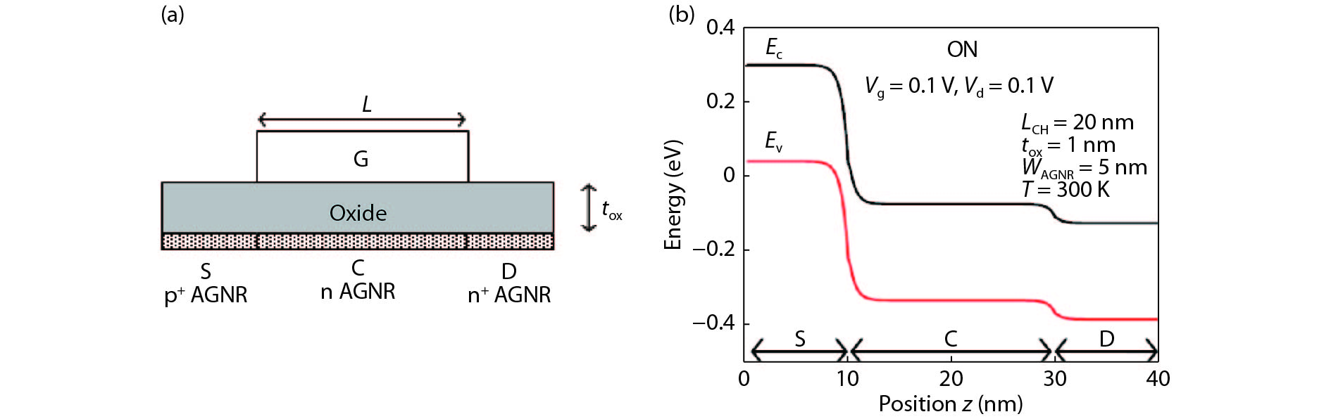
Fig. 1(a) depicts the device structure of the n-channel GNR. We used the armchair graphene nanoribbons (AGNR) type and it is doped to be p+, n, and n+ which used as source, channel and drain, respectively. By solving the Dirac-like Hamilton equation, the Poisson’s equation to consider self-consistently, the potential profile of GNR-TFET was determined. The z-direction was claimed as the finite difference method that was used to discretize the Poisson’s equation and the Dirac-like Hamiltonian along the carrier transport direction,
![]()
Figure 1.(Color online) (a) The device structure of the n-channel GNR-TFET. (b) The conduction band of the GNR-TFET after self-consistency achieved.
From this equation, it can be seen that
The wave function solutions in each region are obtained by applying Eq. (1) to the electron wave function ψ,
where B1, AS, BS, AC, BC, AD, BD and A2 are constants, V is the potential energy, L is the channel length (the source length = the drain length = L/2),
where
3. Calculated result and discussion
The tunneling currents (Id) as a function of drain voltage (Vd) for various gate voltages (Vg) calculated by using Dirac-like equation and Schrödinger equation are depicted in Fig. 2(a). The AGNRs width, channel length L, the insulator (oxide thickness) tox, and the temperature are 5 nm, 20 nm, 1 nm, and 300 K, respectively. The tunneling currents calculated by both equations indicate the same characteristics and the device shows the metal–oxide–semiconductor field-effect transistor (MOSFET) type behavior. It can be seen from the figures that the tunneling currents initially escalate with the drain voltage and they are then able to saturate. If the drain voltage increased continuously with the gate voltage fixed, the number of electrons that tunnel has not increased because the valence band at source and the conduction band in channel does not change with the increase of drain voltage. In this case, the current relatively constant and saturation occurs. Fig. 2(b) reports the tunneling currents (Id) as a function of gate voltage for variety of drain voltages. Furthermore, the tunneling current goes up with the gate voltage. While the gate voltage is added, the conduction band in channel is reduced, so the valence band in source is higher than the conduction band in channel. Electrons stream from valence band at source to conduction band in channel. The tunneling current significantly mounts when the gate voltage escalated. In addition, the tunneling current calculated using Dirac-like equation was lower than those obtained using Schrödinger’s equation.
![]()
Figure 2.(Color online) (a) The tunneling currents as a function of drain voltage for various gate voltages, (b) The tunneling currents as a function of gate voltage for various drain voltages.
Fig. 3(a) displays the tunneling currents as a function of drain voltage for different oxide thicknesses based on Schrödinger and Dirac-like equation. We used the gate voltage 0.1 V and the same parameters as in the other examples. From this figure, it can be inferred that the tunneling current calculated using Dirac-like equation was lower than those obtained using Schrödinger equation. There are significant differences between the tunneling currents that were calculated by using the Dirac-like equation and the Schrödinger equations for the gate voltage 0.1 V. The tunneling current as a function of the drain voltage for diverse oxide thicknesses based on Dirac-like equation has been presented in Fig. 3(b). The tunneling current increases as the thickness of the oxide decreases. When the oxide thickness goes down, the gate capacitance rises. For fixed gate voltage, the amounts of electrons in the channel escalate[
![]()
Figure 3.(Color online) (a) The tunneling currents as a function of drain voltage for various oxide thickness for Schrödinger and Dirac-like equation, (b) The tunneling currents as a function of drain voltage for various oxide thickness for Dirac-like equation.
Fig. 4(a) demonstrates the reliance of the tunneling current on the drain voltage for different AGNR widths. The AGNRs channel length L, the insulator (oxide thickness) tox, the temperature, and the gate voltage are 20 nm, 1 nm, 300 K, and 0.1 V, respectively. It can be seen that the tunneling current goes up as the AGNR width increases. This happens because the AGNR band-gap is inversely proportional to the AGNR width[
![]()
Figure 4.(Color online) (a) The tunneling currents as a function of drain voltage for various AGNR widths. (b) The tunneling currents as a function of gate voltage for various temperatures.
The results that we have obtained suggest that the tunneling current from the calculation using Dirac-like equation is always smaller than the use of Schrödinger’s equation. It is assumed that the Fermi velocity and the effective mass of electrons are the contributing factors because they distinguish the use of Dirac-like and Schrödinger’s equations. The effect of Fermi velocity on the tunneling current characteristics is shown in Fig. 5(a). We applied Dirac-like equations in calculating the tunneling current by taking the Fermi velocity of 106 m/s. This value is greater than the electron Fermi velocity in other materials, such as metal and semiconductors, with a range of values 104_105 m/s. The growing electron Fermi velocity results in smaller tunneling currents, while for the electron Fermi velocity it gets smaller, and the tunneling current that was produced by the AGNR-TFET gets bigger. When the electron Fermi velocity is 104 m/s (red line), the tunneling current calculated using a Dirac-like equation is almost the same as the tunneling current calculated using Schrödinger’s equation. The difference in the tunneling current may also be due to the different approximation of the two equations. This result explains the difference in the tunneling current resulting from the calculations using Dirac-like equation and Schrödinger’s equation.
![]()
Figure 5.(Color online) (a) Characteristics of tunneling currents on gate voltages resulting from the calculation of Dirac-like equations for variations in Fermi velocity (b) Comparison of tunneling current calculated by Schrödinger equation, Dirac-like equation and an experiment by Wang, 2008.
To clarify the results of this calculation, we compared the modeling data with experimental data. For comparison, we use the result of the experiment reported by Wang et al., 2008[
Based on the results of our calculations, we suggest that the calculation method used to model a real device depends on the mobility of carrier (electrons and holes) in the material. A Dirac-like equation (relativistic) can be used to analyze the electron transport process in graphene because the charge carriers in graphene resemble relativistic particles with zero rest mass and effective speed of around c/300[
4. Conclusion
In this paper, we modeled the tunneling current in graphene nanoribbon tunnel field effect transistor (GNR-TFET). The potential profile of GNR-TFET is calculated and found to be self-consistent between the Dirac-like equation and Poisson’s equation, and also Schrödinger’s equation and Poisson’s equation as a comparison. The tunneling current and the electron transmittance are derived by implementing the transfer matrix method (TMM). For comparison, the tunneling current is also calculated using the Schrödinger equation. It is found that the tunneling current increases with the drain voltage and it achieves saturation by applying the calculation of both equations. It has also been found that the AGNR width, the oxide thickness, and the temperature all influence the performance of the GNR-TFET. The tunneling currents increase as the thickness of the oxide decreases and it increases as the AGNR width increases. The tunneling current differences calculated using both equations decrease as the AGNR width increases. Raising the temperatures will decrease the tunneling current. In addition, the tunneling current calculated using Dirac-like equation is lower than those obtained using Schrödinger’s equation. The use of the Dirac-like equation for the Fermi velocity 104 m/s yields a tunneling current that is close to the result calculated with Schrodinger’s equation.
Acknowledgements
This work was supported by Hibah Penelitian Berbasis Kompetensi 2018 RISTEKDIKTI Republic of Indonesia.
References
[1] K S Novoselov, A K Geim, S V Morozov et al. Electric field effect in atomically thin carbon films. Science, 306, 666(2004).
[2] C Berger, Z Song, X Li et al. Electronic confinement and coherence in patterned epitaxial graphene. Science, 312, 1191(2006).
[3] D Jena, T Fang, Q Zhang et al. Zener tunneling in semiconducting nanotube and graphene nanoribbon p−n junctions. Appl Phys Lett, 93, 112106(2008).
[4] W Yansen, M Abdullah. Application of airy function approach to model electron tunneling in graphene nanoribbon-based P−N junction diodes. Journal Nanosains & Nanoteknologi, 3, 18(2010).
[5] L Brey, H A Fertig. Electronic states of graphene nanoribbons. Phys Rev, B73, 235411(2006).
[6] Y W Son, M L Cohen, S G Loui. Energy gaps in graphene nanoribbons. Phys Rev Lett, 97, 216803(2006).
[7] B Huang, Q Yan, G Zhou et al. Making a field effect transistor on a single graphene nanoribbon by selective doping. Appl Phys Lett, 91, 253122(2007).
[8] J Knoch, J Appenzeller. Tunneling phenomena in carbon nanotube field-effect transistors. Phys. Status Solidi A, 205, 679(2008).
[9] M I Katsnelson, K S Novoselov, A K Geim. Chiral tunneling and the Klein paradox in graphene. Nat Phys, 2, 620(2006).
[10] E Suhendi, R Syariati, F A Noor et al. Simulation of Dirac tunneling current of an armchair graphene nanoribbon-based p–n junction using a transfer matrix method. Adv Mater Res, 974, 205(2014).
[11] V Hung Nguyen, A Bournel, P Dollfus. Large peak-to-valley ratio of negative-differential-conductance in graphene p–n junctions. J Appl Phys, 109, 093706(2011).
[12] P Nam Do, P Dollfus. Negative differential resistance in zigzag-edge graphene nanoribbon junction. J Appl Phys, 107, 063705(2010).
[13] X Xu, G Xu, J Cao. Electron tunneling through a trapezoidal barrier in graphene. Jpn J Appl Phys, 49, 085201(2010).
[14] E Suhendi, R Syariati, F A Noor et al. Modeling of Dirac electron tunneling current in bipolar transistor based on armchair graphene nanoribbon using a transfer matrix method. Adv Comput Sci Res, 5, 164(2015).
[15] J Chauhan, J Guo. Assessment of high-frequency performance limits of graphene field-effect transistors. Nano Res, 4, 571(2011).
[16] U Mukherjee, S Banerjee, R Sarkar et al. Single quantum well p–n junction diode based on graphene nanoribbon. Graphene, 3, 6(2015).
[17] Y Khatami, J Kang, K Banerjee. Graphene nanoribbon based negative resistance device for ultra-low voltage digital logic applications. App Phys Lett, 102, 043114(2013).
[18] M Noei, M Moradinasab, M Fathipour. A computational study of ballistic graphene nanoribbon field effect transistors. Phys E, 44, 1780(2012).
[19] X Yang, J Chauhan, J Guo et al. Graphene tunneling FET and its applications in low-power circuit design. Proc of the 20th symposium on Great lakes symposium on VLSI, 263(2010).
[20] Q Zhang, T Fang, H Xing et al. Graphene nanoribbon tunnel transistors. Electron Device Lett, 29, 1344(2008).
[21] T M Abdolkader, M H Hassan, W Fikry. Solution of Schrödinger equation in double-gate MOSFETs using transfer matrix method. Electron Lett, 40, 20(2004).
[22] F A Noor, M Abdullah et al. Comparison of electron transmittances and tunneling currents in an anisotropic TiN
[23] W Z Shangguan, X Zhou, S B Chiah et al. Compact gate-current model based on transfer-matrix method. J Appl Phys, 97, 123709(2005).
[24] K W Terrill, C Hu, P K Ko. An analytical model for the channel electric field in MOSFETs with graded-drain structures. IEEE Electron Device Lett, 5, 440(1984).
[25]
[26] M Tiwari, K K Sharma, L S Rawat et al. Impact of oxide thickness on gate capacitance, drain current and transconductance – a comprehensive analysis on MOSFET, nanowire FET and CNTFET devices. Int J Res Emerg Sci Technol, 2, 73(2015).
[27] K I Bolotin, K J Sikes et al. Ultrahigh electron mobility in suspended graphene. Solid State Commun, 146, 351(2008).
[28] X Du, I Skachko, A Barker et al. Approaching ballistic transport in suspended graphene. Nature Nanotechnol, 3, 491(2008).
[29]
[30] X Wang, Y Ouyang, X Li et al. Room-temperature all-semiconducting sub-10-nm graphene nanoribbon field-effect transistors. Phys Rev Lett, 100, 206803(2008).
[31] D Jimenez. A current-voltage model for Schottky-barrier graphene based transistors. Nanotechnology, 19, 345204(2008).

Set citation alerts for the article
Please enter your email address
© Copyright 2018-2021 | Chinese Laser Press. All Rights Reserved 沪ICP备15018463号-20