
Junyan Li, Na Qian, Shiyu Hua, Weiwen Zou. Optimization of optical signal-to-distortion ratio in a channel-interleaved photonic ADC via a coherent multi-frequency RF driver[J]. Chinese Optics Letters, 2021, 19(8): 083901
- Chinese Optics Letters
- Vol. 19, Issue 8, 083901 (2021)
Abstract
Keywords
1. Introduction
With the increasing demand for high-speed sampling technology, photonic analog-to-digital converter (PADC) technology is regarded as an ideal solution that can overcome the bottleneck faced by electronic analog-to-digital converters (EADCs)[
On the other hand, the technology of RF modules with a single or multichip is mature[
2. Principles
In this Letter, we analyze the relationship between the characteristics of RF driver signals and the performance of a time-domain channel-interleaved demultiplexer based on photonic switches. The optical signal-to-distortion ratio (OSDR) is regarded as the most effective parameter to evaluate the demultiplexer performance. A multi-frequency RF driver is designed for the optimization of the OSDR in the PADC system. In our design, low noise amplifiers (LNAs), power amplifiers (PAs), variable attenuators (VAs), and variable phase shifters (VPSs) are cascaded to obtain sufficient gain and well-managed amplitude and phase. Then, the RF driver is applied in an eight-channel PADC system with a sampling rate of 40 GSa/s. The performance is verified in the demultiplexer of the sampling series.
Sign up for Chinese Optics Letters TOC. Get the latest issue of Chinese Optics Letters delivered right to you!Sign up now
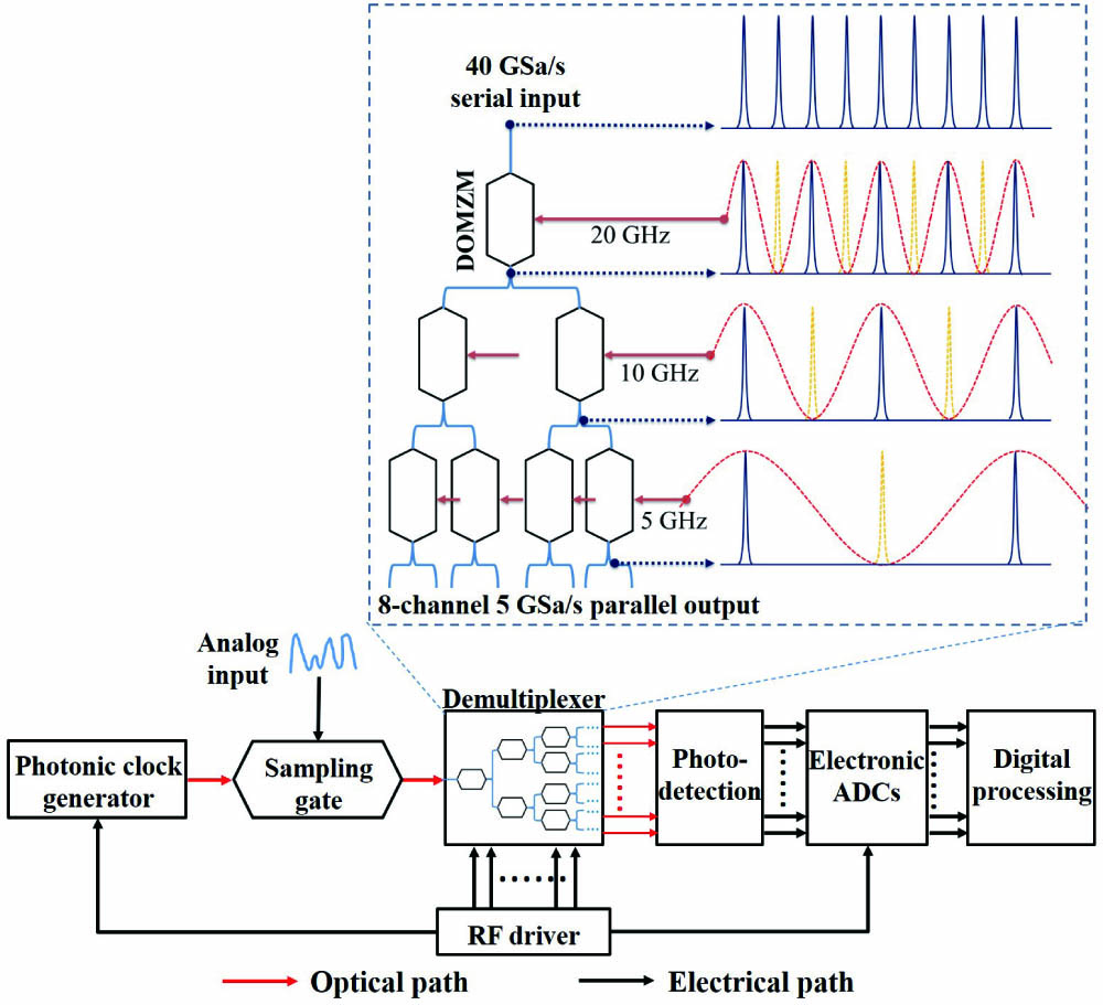
A schematic of an eight-channel 40 GSa/s PADC system with a channel-interleaved demultiplexer based on photonic switches is illustrated in Fig. 1. In this scheme, an actively mode locked laser (AMLL) with a high repetition rate serves as a photonic sampling clock generator, and a Mach–Zehnder modulator (MZM) is used as a sampling gate. For the demultiplexer, an array of dual-output MZMs (DOMZMs) is applied as the photonic switches. The demultiplexed series are detected via photodiodes (PDs) and then digitized by EADCs for digital processing.
![]()
Figure 1.Schematic of a 40 GSa/s eight-channel PADC with a channel-interleaved demultiplexer based on a binary tree of dual-output Mach–Zehnder modulators (DOMZMs). The inset shows the working mechanism of a three-class demultiplexer, which converts sampling series of 40 GSa/s into eight parallel channels of 5 GSa/s.
The topological structure of the demultiplexer can be considered as a binary tree of DOMZMs. In this structure, two DOMZMs are connected to each output port of the DOMZM in the previous class. A three-class cascaded scheme is shown in the inset of Fig. 1, which can convert the sampling series of 40 GSa/s into eight parallel channels with the speed of 5 GSa/s. In the channel-interleaved demultiplexer, the DOMZM in the first class is driven by an RF signal of 20 GHz, and the frequencies of the driver signals are 10 GHz and 5 GHz for the second and third classes, respectively.
The parameters of each RF signal should be properly managed. In mathematics, the conclusion in Ref. [17] can be extended to multi-channel cases. As for a demultiplexer consisting of multiple classes of DOMZMs, the switching response of one DOMZM in the Kth class can be expressed as
In a three-class DOMZM-based demultiplexer, one of the demultiplexed series from the output of th-class DOMZM can be expressed as
![]()
Figure 2.(a) Schematic of the selected pulse and induced distortions in a three-class DOMZM-based demultiplexer. αK is the switching response of one DOMZM in the Kth class (K = 1, 2, 3), IS is the intensity of the selected pulse, and ID,K is the intensity of the distortions induced in the Kth class. (b) Simulated optical signal-to-distortion ratio (OSDR) at each single-class DOMZM versus both amplitude and phase offsets of the RF driver signal. The colors on the surface refer to the magnitude of the OSDRK. The subscript K represents an integer, which can be 1, 2, or 3.
According to Eqs. (6) and (7), to achieve an optimized OSDR, each should be maximized. Since and are inherent characteristics of DOMZMs, the demultiplexing modulation in Eq. (2) should be maximized in each class. It is obvious that the ideal condition can achieve the maximum OSDR, which is , corresponding to and .
To investigate the effect of the parameters of RF driver signals, their amplitude and phase can be normalized as
3. RF Driver Design
As for the demultiplexer, a DOMZM (EOSpace AX-1x2-0MSS-40) of 40 GHz is used as the photonic switch working at 20 GHz in the first class. In the second class, two DOMZMs (EOSpace AX-1x2-0MSS-10) of 10 GHz working at 10 GHz are applied. In the third class, four DOMZMs (EOSpace AX-1x2-0MSS-10) of 10 GHz working at 5 GHz are adopted. According to the transmission curve of the DOMZMs, the AC half-wave voltages for each class are measured to be 5.8 V at 20 GHz, 5.1 V at 10 GHz, and 4.3 V at 5 GHz, respectively. The half-wave voltages are determined by the maximum and minimum output intensities of each DOMZM. As the match impedance is , the power at in Eq. (8) should be , namely 19.3 dBm for the signal of 20 GHz in the first class, 18.2 dBm for each signal of 10 GHz in the second class, and 16.7 dBm for each signal of 5 GHz in the third class. As for the phase offset, the ideal condition can be determined by the intensity of the pulse, which is selected to pass and reaches its maximum. In practice, the channel-interleaved demultiplexer is not the only component that requires RF signals in the PADC system, as illustrated in Fig. 1. The AMLL should be seeded to generate the photonic sampling clock at 40 GHz. The EADCs should be triggered to perform the digitization at 5 GHz. All RF signals should be synchronized for coherence.
According to the requirements of RF signals, we design a microwave chain using commercial chips, as shown in Fig. 3(a). In this scheme, the chain adopts a signal of 20 GHz with a power of 0 dBm as the original input, which is divided into four paths by two-class cascaded power splitters (PSs). For the first path, through an LNA (WFD180240-L17) and a frequency multiplier (FM, WBD220440-B2), a signal of 40 GHz with a maximum power of 14 dBm is achieved to seed the AMLL. The signal in the second path is directly amplified to 6 dBm by an LNA (WFD180240-L17) and then reaches the maximum power at 25 dBm by a PA (WFD196220-P25). It is used as the driver signal of 20 GHz in the first class. The frequency of the signal in the third path is first divided into 10 GHz by a frequency divider (FD, HMC492LP3). The signal is amplified to 18 dBm by an LNA (WFD060180-L18) and split into two outputs by a PS (microstrip line), which is further amplified to 24 dBm in the maximum by PAs (WFD080120-P24) to drive the DOMZMs in the second class. As for the fourth path, the frequency of the signal is divided into 5 GHz by an FD (HMC493LP3). The signal splits into five outputs. Among them, four are amplified to 20 dBm in the maximum by LNAs (WFD020060-L10) and PAs (WFD020060-P26) in sequence for the DOMZMs in the third class, and one is amplified to 10 dBm by an LNA (WFD020060-L10) to serve as the trigger clock for the EADCs. Besides, all the output signals are filtered via band-pass filters (BPF), VAs, and VPSs, to guarantee good waveform and precise adjustment of both amplitude and phase of the output signals.
![]()
Figure 3.(a) Design schematic of the microwave-chip-based RF driver and (b) its photo. PS, power splitter; LNA, low noise amplifier; PA, power amplifier; FM, frequency multiplier; FD, frequency divider; VA, variable RF attenuator; VPS, variable RF phase shifter; BPF, band-pass filter; EADC, electronic ADC.
In implementation, the module includes a front board for RF components and a back board for DC bias. The metal box is used to support the boards and guarantee the performance under various conditions. The size of the module is , as shown Fig. 3(b). It should be noted that there are three paths of seed signals of 40 GHz and two paths of the trigger clock at 5 GHz. The redundant outputs are reserved for the synchronization of peripherals in potential applications.
In terms of performance of the RF driver module, the input bandwidth is 18–22 GHz. Figures 4(a)–4(d) show the typical responses of the output ports of the RF driver module with different frequencies, which are measured by a spectrum analyzer (R&S FSW43). By adjusting the VAs, we can obtain different power. The effect in the phase shift can be observed from the results of the demultiplexer. The adjustment precisions in power and phase shifts are 0.5 dB (6 bits) and 5.6° (6 bits), respectively, depending on the specifications of VAs and VPSs. The spectra of generated RF signals after adjustments are measured, as shown in Figs. 4(e)–4(h). From these spectra, it can be found that the amplitudes of these signals can match well with the requirements of the demultiplexer. These spur-free spectra also indicate good sinusoidal temporal waveforms. In this situation, the power consumption of the module is 15.8 W.
![]()
Figure 4.(a)–(d) Typical frequency responses of the output ports of the RF driver module with different frequencies and different power. The adjustment precision in power is 0.5 dB and 6 bits. The working frequencies and power are marked as black dots. (e)–(h) The spectra of the output driver signal from the ports in (a)–(d). All plots are marked with the frequency and the power.
4. Experiments
The RF driver module is further applied in a 40 GSa/s PADC for laboratory test. In this system, the AMLL (Calmar PSL-40-1 T) is successfully seeded by the RF driver to generate a sampling clock of 40 GSa/s, which is channel-interleaved by the demultiplexer based on three-class DOMZMs. The demultiplexing performance in each class is tested and optimized one by one based on the adjustment of the amplitude and phase of RF driver signals. Figure 5 shows the temporal waveforms of the demultiplexed series of each class under different conditions of RF driver signals. The waveforms are captured by a sampling oscilloscope (Agilent DCA-X 86100D). Only one channel is illustrated as a representative of each class. It can be found that the series of 40 GSa/s is demultiplexed into series of 20 GSa/s, 10 GSa/s, and 5 GSa/s after each class, respectively. In Figs. 5(a)–5(i), the amplitude and phase offsets of RF driver signals in each class are marked along with the measured waveforms. To evaluate the demultiplexing performance in each class, the can be calculated with the measured peak intensity of the pulses in Figs. 5(a)–5(i) according to the definition in Eq. (6). The theoretical estimation can also be derived from Eq. (6) based on the amplitude and phase offsets. Figure 5(j) depicts the in each class, which are calculated from the waveforms in Figs. 5(a)–5(i). Note that the maximum and minimum transmittances of DOMZMs are 0.5 dB and 25 dB, respectively. The theoretical estimations are derived from Eq. (6) and compared with the experimentally measured results.
![]()
Figure 5.Temporal waveforms of demultiplexed series from each class under different conditions of the amplitude and phase of RF driver signals in (a)–(c) first class, (d)–(f) second class, and (g)–(i) third class. (j) Comparison between the theoretically estimated and the experimentally measured OSDRK according to (a)–(i). The measured values are labeled, and the contours are based on the theoretical model.
From Fig. 5(j), it can be found that the values of increase from to in all three classes along with suppressed amplitude and phase offsets. The feasibility of the theoretical analysis in Eq. (6) can be verified from the consistence between the measured and estimated results. Furthermore, the final demultiplexed 5 GSa/s series under different conditions of amplitude and phase of the RF driver signals applied in each class [i.e., the cases shown in Figs. 5(a)–5(i)] are depicted in Fig. 6. The values of OSDRs are calculated from the waveforms and compared with their estimation derived from Eq. (7) based on the values of in each class. A good consistence also verifies the analysis in Eq. (7). In these cases, Fig. 6(a) depicts the temporal waveforms of final demultiplexed series with , , and according to Figs. 5(a), 5(d), and 5(g), respectively. Similarly, Fig. 6(b) depicts the temporal waveforms of final demultiplexed series according to Figs. 5(b), 5(e), and 5(h). Figure 6(c) depicts the temporal waveforms of the final demultiplexed series according to Figs. 5(c), 5(f), and 5(i). The OSDR of the final demultiplexed series increases with the in each class, as shown in Figs. 6(a)–6(c). The best measurable OSDR of the final demultiplexed series after three classes of DOMZMs reaches with a voltage detection precision of . Furthermore, the precision can be further improved by eliminating the noise with ultra-high-speed real-time oscilloscopes through heterodyne detection and the averaging method. Without an EADC, the OSDR is considered as the most effective parameter to evaluate the performance of the demultiplexer. As the OSDR increases, the improvement in the performance of the PADC can be evaluated by the effective number of bits (ENOB). The relationship between the OSDR and the ENOB will be studied in future research.
![]()
Figure 6.Temporal waveforms of final demultiplexed 5 GSa/s series under the conditions depicted in Figs.
5. Conclusion
A microwave-chip-based coherent multi-frequency RF driver module is developed and applied to the channel-interleaved demultiplexer in a PADC system of 40 GSa/s. We theoretically analyze the relationship between the characteristics of generated RF driver signals and demultiplexing performance. In laboratory test, a beam sampling series of 40 GSa/s is converted into eight parallel channels of 5 GSa/s with RF driver signals, which drive the photonic switches. By precisely adjusting the amplitude and phase of these signals, the OSDR is optimized. The results verify the compatibility between the RF driver and the PADC system. With its compact size, the RF driver is considered as one step towards practical application and the next-generation of PADC systems in a module or on a chip.
References
[1] G. C. Valley. Photonic analog-to-digital converters. Opt. Express, 15, 1955(2007).
[2] P. W. Juodawlkis, J. C. Twichell, G. E. Betts, J. J. Hargreaves, R. D. Younger, J. L. Wasserman, F. J. O’Donnell, K. G. Ray, R. C. Williamson. Optically sampled analog-to-digital converters. IEEE Trans. Microwave Theroy Tech., 49, 1840(2001).
[3] Y. Han, B. Jalali. Photonic time-stretched analog-to-digital converter: fundamental concepts and practical considerations. J. Lightwave Technol., 21, 3085(2003).
[4] A. Khilo, S. J. Spector, M. E. Grein, A. H. Nejadmalayeri, C. W. Holzwarth, M. Y. Sander, M. S. Dahlem, M. Y. Peng, M. W. Geis, N. A. DiLello, J. U. Yoon, A. Motamedi, J. S. Orcutt, J. P. Wang, C. M. Sorace-Agaskar, M. A. Popović, J. Sun, G. Zhou, H. Byun, J. Chen, J. L. Hoyt, H. I. Smith, R. J. Ram, M. Perrott, T. M. Lyszczarz, E. P. Ippen, F. X. Kärtner. Photonic ADC: overcoming the bottleneck of electronic jitter. Opt. Express, 20, 4454(2012).
[5] T. R. Clark, J. U. Kang, R. D. Esman. Performance of a time- and wavelength-interleaved photonic sampler for analog-digital conversion. IEEE Photon. Technol. Lett., 11, 1168(1999).
[6] R. Williamson, P. Juodawlkis, J. Wasserman, G. Betts, J. Twichell. Effects of crosstalk in demultiplexers for photonic analog-to-digital converters. J. Lightwave Technol., 19, 230(2001).
[7] G. Yang, W. Zou, L. Yu, K. Wu, J. Chen. Compensation of multi-channel mismatches in high-speed high-resolution photonic analog-to-digital converter. Opt. Express, 24, 24061(2016).
[8] H. Zhang, W. Zou, G. Yang, J. Chen. Dual-output modulation in time-wavelength interleaved photonic analog-to-digital converter based on actively mode-locked laser. Chin. Opt. Lett., 14, 030602(2016).
[9] G. Yang, W. Zou, Y. Yuan, J. Chen. Wideband signal detection based on high-speed photonic analog-to-digital converter. Chin. Opt. Lett., 16, 030601(2018).
[10] F. Yang, W. Zou, L. Yu, S. Xu, J. Chen. Impact of optical–electrical conversion responsivity in sub-sampled photonic analog-to-digital converter. Chin. Opt. Lett., 17, 040602(2019).
[11] K. Zheng, W. Zou, L. Yu, N. Qian, J. Chen. Stability optimization of channel-interleaved photonic analog-to-digital converter by extracting of dual-output photonic demultiplexing. Chin. Opt. Lett., 18, 012502(2020).
[12] S. Xu, X. Zou, B. Ma, J. Chen, L. Yu, W. Zou. Deep-learning-powered photonic analog-to-digital conversion. Light: Sci. Appl., 8, 41377(2019).
[13] R. Wang, S. Xu, J. Chen, W. Zou. Ultra-wideband signal acquisition by use of channel-interleaved photonic analog-to-digital converter under the assistance of dilated fully convolutional network. Chin. Opt. Lett., 18, 123901(2020).
[14] G. Yang, W. Zou, X. Li, J. Chen. Theoretical and experimental analysis of channel mismatch in time-wavelength interleaved optical clock based on mode locked laser. Opt. Express, 23, 2174(2015).
[15] F. Scotti, F. Laghezza, S. Pinna, P. Ghelfi, A. Bogoni. High precision photonic ADC with four time-domain-demultiplexed interleaved channels. OptoElectronics and Communications Conference and Photonics in Switching, TuO1_3(2013).
[16] G. Yang, W. Zou, L. Yu, J. Chen. Investigation of electronic aperture jitter effect in channel-interleaved photonic analog-to-digital converter. Opt. Express, 27, 9205(2019).
[17] L. Yu, W. Zou, G. Yang, X. Li, J. Chen. Switching response of dual-output Mach–Zehnder modulator in channel-interleaved photonic analog-to-digital converter. Chin. Opt. Lett., 16, 120602(2018).
[18] N. Qian, L. Yu, J. Chen, W. Zou. Influence of the demultiplexer on channel-interleaved photonic analog-to-digital converters. IEEE Photon. J., 12, 5502110(2020).
[19] R. Gugulothu, S. V. Bhalke, A. A. Naik, K. Lalkishore, R. Dasari. Multi-chip module based GaAs MMICs packaging for L-band high gain application. IEEE MTT-S International Microwave and RF Conference, 1(2019).
[20] Y. Zhang, S. Shi, R. Martin, A. Wright, P. Yao, K. Shreve, C. Harrity, D. Prather. Packaging of high-gain multichip module in multilayer LCP substrates at W-band. IEEE Trans. Compon. Packag. Manuf. Technol., 7, 1655(2017).

Set citation alerts for the article
Please enter your email address
© Copyright 2018-2021 | Chinese Laser Press. All Rights Reserved 沪ICP备15018463号-20