• Photonics Research
  • Vol. 7, Issue 4, 473 (2019)
Erwen Li, Behzad Ashrafi Nia, Bokun Zhou, and Alan X. Wang*
Author Affiliations
  • School of Electrical Engineering and Computer Science, Oregon State University, Corvallis, Oregon 97331, USA
  • show less
    DOI: 10.1364/PRJ.7.000473 Cite this Article Set citation alerts
    Erwen Li, Behzad Ashrafi Nia, Bokun Zhou, Alan X. Wang. Transparent conductive oxide-gated silicon microring with extreme resonance wavelength tunability[J]. Photonics Research, 2019, 7(4): 473 Copy Citation Text show less
    (a) Cross-sectional and (b) top view schematic of the hybrid TCO–silicon tunable microring filter. (c) Simulated tunability (solid lines) and Q-factor (dashed lines) of the tunable microring filters as functions of the waveguide width. Two different thicknesses of gate oxide layer are simulated (16 nm of HfO2 and 5 nm of HfO2). (d) and (e) Simulated cross-sectional electrical energy (ε|E|2) distribution of the microring filter at different waveguide widths of 300 and 400 nm, respectively. Zoomed-in views of the distributions in the interface region (white dashed box) are plotted on the right.
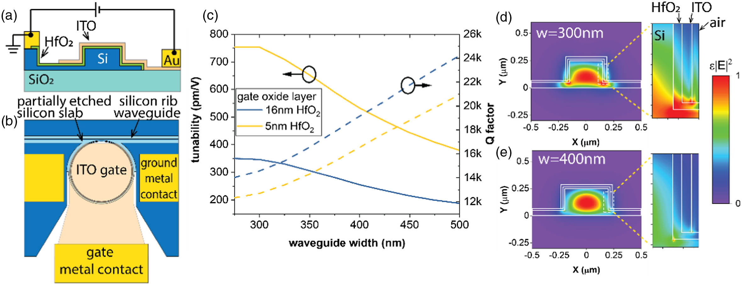
    Fig. 1. (a) Cross-sectional and (b) top view schematic of the hybrid TCO–silicon tunable microring filter. (c) Simulated tunability (solid lines) and Q-factor (dashed lines) of the tunable microring filters as functions of the waveguide width. Two different thicknesses of gate oxide layer are simulated (16 nm of HfO2 and 5 nm of HfO2). (d) and (e) Simulated cross-sectional electrical energy (ε|E|2) distribution of the microring filter at different waveguide widths of 300 and 400 nm, respectively. Zoomed-in views of the distributions in the interface region (white dashed box) are plotted on the right.
    (a) Optical image of a fabricated tunable microring filter with a radius of 12 μm. The ITO gate (highlighted by a red line) covers the majority of the microring except the coupling region. The ground electrodes are connected to the silicon ring through a partially etched silicon slab. (b) Scanning electron micrograph (SEM) of the fabricated silicon microring, showing side-wall roughness after the RIE process.
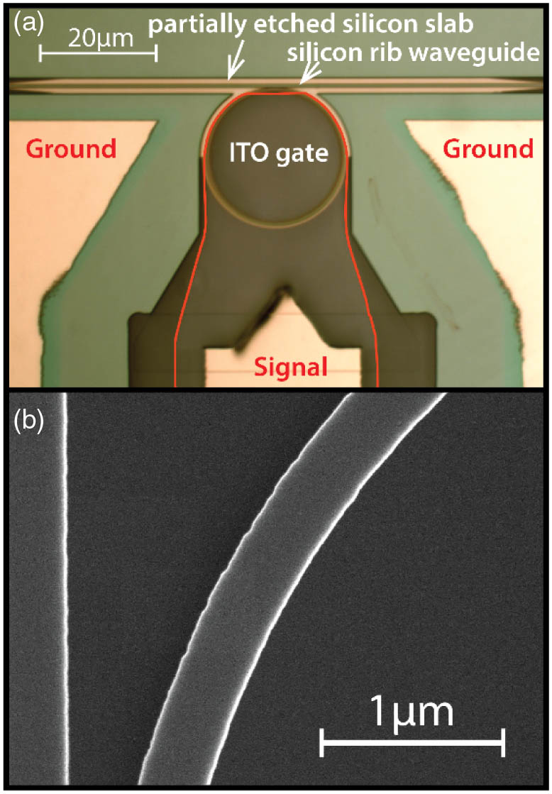
    Fig. 2. (a) Optical image of a fabricated tunable microring filter with a radius of 12 μm. The ITO gate (highlighted by a red line) covers the majority of the microring except the coupling region. The ground electrodes are connected to the silicon ring through a partially etched silicon slab. (b) Scanning electron micrograph (SEM) of the fabricated silicon microring, showing side-wall roughness after the RIE process.
    (a) Measured transmission spectra of a tunable microring filter under different applied gate biases. The microring has a waveguide width of 300 nm and a HfO2 gate oxide layer thickness of 16 nm. (b) Resonance shift (blue line, left axis) and Q-factor (red line, right axis) of the microring filter as functions of applied gate bias. (c) Simulated Q-factor of a microring with a waveguide width of 300 nm and 16 nm of HfO2 gate oxide as a function of applied bias.
    Fig. 3. (a) Measured transmission spectra of a tunable microring filter under different applied gate biases. The microring has a waveguide width of 300 nm and a HfO2 gate oxide layer thickness of 16 nm. (b) Resonance shift (blue line, left axis) and Q-factor (red line, right axis) of the microring filter as functions of applied gate bias. (c) Simulated Q-factor of a microring with a waveguide width of 300 nm and 16 nm of HfO2 gate oxide as a function of applied bias.
    Leakage current density of a testing Si/HfO2/Au MOS capacitor as a function of applied voltage with a 16-nm-thick HfO2 gate oxide layer.
    Fig. 4. Leakage current density of a testing Si/HfO2/Au MOS capacitor as a function of applied voltage with a 16-nm-thick HfO2 gate oxide layer.
    (a) Voltage swing of 0 to −3 V applied on the tunable microring filter. (b) Output response of the microring filter. (c) and (d) Rising and falling edge of the output in (b), respectively.
    Fig. 5. (a) Voltage swing of 0 to 3  V applied on the tunable microring filter. (b) Output response of the microring filter. (c) and (d) Rising and falling edge of the output in (b), respectively.
    Erwen Li, Behzad Ashrafi Nia, Bokun Zhou, Alan X. Wang. Transparent conductive oxide-gated silicon microring with extreme resonance wavelength tunability[J]. Photonics Research, 2019, 7(4): 473
    Download Citation