
Chengcheng Huang, Yonggang Zhang, Lanju Liang, Haiyun Yao, Wenjia Liu, Fu Qiu. Narrow/Broad Band Switchable Terahertz Absorber Based on Graphene and Vanadium Dioxide Composite Structure[J]. Acta Optica Sinica, 2022, 42(19): 1916001
- Acta Optica Sinica
- Vol. 42, Issue 19, 1916001 (2022)
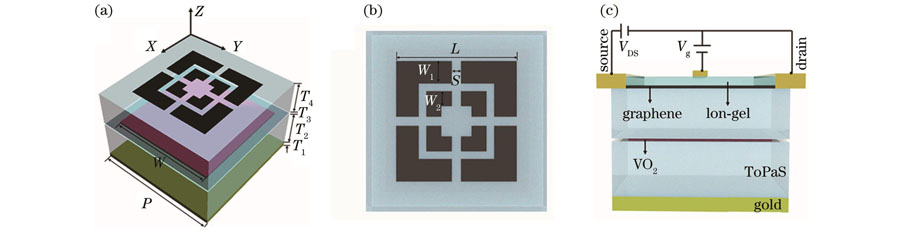
Fig. 1. Schematic diagrams of absorber unit cell. (a) Side view of unit cell; (b) top view of unit cell; (c) schematic of applying voltage to graphene
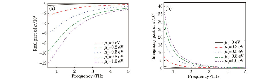
Fig. 2. Conductivity of graphene at different Fermi levels. (a) Real part of conductivity; (b) imaginary part of conductivity
Fig. 3. Simulated absorption spectra of absorber under different VO2 states
Fig. 4. Absorption spectra and relative impedance of absorbers under different VO2 states. (a) Metallic state; (b) insulating state
Fig. 5. Distributions of surface current and magnetic field of YOZ plane. (a)(e)(i)(m) Current distributions of graphene at four frequency points; (b)(f)(j)(n) current distributions of VO2 at four frequency points; (c)(g)(k)(o) current distributions of metal substrate of structure at four frequency points; (d)(h)(l)(p) magnetic field distributions of air above graphene structure at four frequency points
Fig. 6. Absorption spectra of absorber under different Fermi levels of graphene and different conductivity of VO2. (a) Absorption spectra under different Fermi levels of graphene; (b) absorption spectra under different conductivities of VO2; (c) absorption spectra for varying both conductivity of VO2 and Fermi levels of graphene
Fig. 7. Absorption spectra of absorber with different polarization angles
Fig. 8. Absorption spectra of absorber at different incident angles,and distributions of magnetic field on YOZ plane with different polarization modes and different incident angles at frequency of 0.99 THz. (a) Absorption spectrum for TE polarization; (b) absorption spectrum for TM polarization; (c) distributions of magnetic field on YOZ plane with different polarization modes and different incident angles at frequency of 0.99 THz
Fig. 9. Absorption characteristics for different refractive indices of object to be measured and absorber sensitivity; (a) Absorption characteristics for different refractive indices of object to be measured; (b) absorber sensitivity
|
Table 1. Absorption characteristics of absorber under different Fermi levels
|
Table 2. Performance comparison between different absorbers

Set citation alerts for the article
Please enter your email address
© Copyright 2018-2021 | Chinese Laser Press. All Rights Reserved 沪ICP备15018463号-20