• Photonics Research
  • Vol. 7, Issue 1, 89 (2019)
Jinchao Tong1、2, Yue Qu2、3, Fei Suo1, Wei Zhou2, Zhiming Huang2、4、5、*, and Dao Hua Zhang1、6、*
Author Affiliations
  • 1School of Electrical and Electronic Engineering, Nanyang Technological University, Singapore 639798, Singapore
  • 2State Key Laboratory of Infrared Physics, Shanghai Institute of Technical Physics, Chinese Academy of Sciences, Shanghai 200083, China
  • 3University of Chinese Academy of Sciences, Beijing 100049, China
  • 4Key Laboratory of Space Active Opto-electronics Technology, Shanghai Institute of Technical Physics, Chinese Academy of Sciences, Shanghai 200083, China
  • 5e-mail: zmhuang@mail.sitp.ac.cn
  • 6e-mail: EDHZHANG@ntu.edu.sg
  • show less
    DOI: 10.1364/PRJ.7.000089 Cite this Article Set citation alerts
    Jinchao Tong, Yue Qu, Fei Suo, Wei Zhou, Zhiming Huang, Dao Hua Zhang. Antenna-assisted subwavelength metal–InGaAs–metal structure for sensitive and direct photodetection of millimeter and terahertz waves[J]. Photonics Research, 2019, 7(1): 89 Copy Citation Text show less
    Schematic of the antenna-assisted subwavelength ohmic Au–InGaAs–Au photodetector (not drawn to scale). (a) Full view of the schematic of the photodetector. (b) Scanning electron microscope image of the fabricated device with wire bonding. The scale bar represents 1 mm. (c) The zoom in tridimensional view for the central part of the structure. L is the length of the semiconductor, and s is the spacing between the edges of the two ohmic contacts. W and t are the width and thickness of the InGaAs layer, respectively. The left-bottom inset is the cross section of the In0.53Ga0.47As/InP detector.
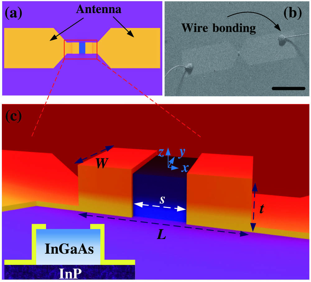
    Fig. 1. Schematic of the antenna-assisted subwavelength ohmic Au–InGaAs–Au photodetector (not drawn to scale). (a) Full view of the schematic of the photodetector. (b) Scanning electron microscope image of the fabricated device with wire bonding. The scale bar represents 1 mm. (c) The zoom in tridimensional view for the central part of the structure. L is the length of the semiconductor, and s is the spacing between the edges of the two ohmic contacts. W and t are the width and thickness of the InGaAs layer, respectively. The left-bottom inset is the cross section of the In0.53Ga0.47As/InP detector.
    Numerical simulations for the antenna-assisted subwavelength Au/Sn–InGaAs–Au/Sn structure. Excitation of localized SPPs, the distribution of E2/E02 along the white dashed line for the incident radiation of ∼0.0375 THz in (a) the bare InGaAs slab (L=150 μm, W=50 μm, and t=10 μm), (b) the subwavelength Au/Sn–InGaAs–Au/Sn structure (the same InGaAs slab with s=90 μm), and (c) the antenna-assisted subwavelength Au/Sn–InGaAs–Au/Sn structure with s=90 μm. (d) Localized-SPP intensity (E2/E02) of the device in (c) as a function of incident power at 0.0375 THz. (e) SPP intensity of the device at different polarization angles for irradiation of 0.0375 THz at the point (s/2, 0, 0). (f) SPP intensity E2/E02 along the half-width line for devices with spacings s of 10, 30, 50, 70, 90, and 110 μm. Inset: E2/E02 as a function of s.
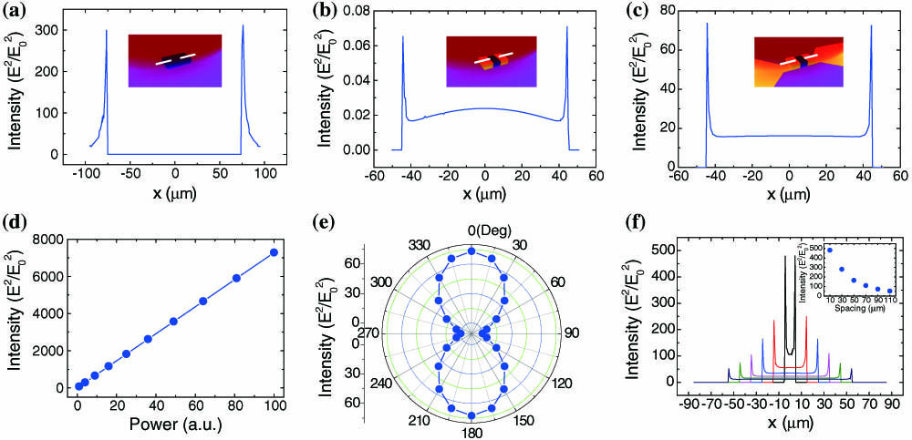
    Fig. 2. Numerical simulations for the antenna-assisted subwavelength Au/Sn–InGaAs–Au/Sn structure. Excitation of localized SPPs, the distribution of E2/E02 along the white dashed line for the incident radiation of 0.0375  THz in (a) the bare InGaAs slab (L=150  μm, W=50  μm, and t=10  μm), (b) the subwavelength Au/Sn–InGaAs–Au/Sn structure (the same InGaAs slab with s=90  μm), and (c) the antenna-assisted subwavelength Au/Sn–InGaAs–Au/Sn structure with s=90  μm. (d) Localized-SPP intensity (E2/E02) of the device in (c) as a function of incident power at 0.0375 THz. (e) SPP intensity of the device at different polarization angles for irradiation of 0.0375 THz at the point (s/2, 0, 0). (f) SPP intensity E2/E02 along the half-width line for devices with spacings s of 10, 30, 50, 70, 90, and 110 μm. Inset: E2/E02 as a function of s.
    Schematic of the optical measurement setup.
    Fig. 3. Schematic of the optical measurement setup.
    Characterization of the antenna-assisted subwavelength Au/Sn–InGaAs–Au/Sn devices. (a) Photovoltage of the device with s=90 μm under 10 mW illumination of a 0.0375 THz source at a modulation frequency of 2000 Hz, as a function of DC bias current. Inset is a typical I–V characteristic curve of the device. The derived resistance is ∼108 Ω. (b) Photovoltage of the same device as a function of source output power at 2000 Hz under a DC bias of 2 mA. (c) Polarization dependence of the photovoltage of the device measured under a DC bias of 2 mA and at the source output power of 10 mW. The vertical and horizontal axes are designated as x and y, respectively. (d) Photovoltages of devices with different values of spacing, measured in the same conditions as for the device with a spacing of 90 μm.
    Fig. 4. Characterization of the antenna-assisted subwavelength Au/Sn–InGaAs–Au/Sn devices. (a) Photovoltage of the device with s=90  μm under 10 mW illumination of a 0.0375 THz source at a modulation frequency of 2000 Hz, as a function of DC bias current. Inset is a typical IV characteristic curve of the device. The derived resistance is 108  Ω. (b) Photovoltage of the same device as a function of source output power at 2000 Hz under a DC bias of 2 mA. (c) Polarization dependence of the photovoltage of the device measured under a DC bias of 2 mA and at the source output power of 10 mW. The vertical and horizontal axes are designated as x and y, respectively. (d) Photovoltages of devices with different values of spacing, measured in the same conditions as for the device with a spacing of 90 μm.
    Relative spectral response of the devices in a different frequency range (normalized value). Response of the device designed for (a) ∼0.0375 THz and (b) ∼0.166 THz. The red lines in (a) and (b) are for a better view. The inset of (b) is the schematic of the log-period antenna device. The red arrow represents the polarization direction of the electric field component of incident light. (c) Response of the device shown in (b) under radiation at around the bandgap energy of the InGaAs semiconductor. The arrow indicates the cutoff (bandgap) of In0.53Ga0.47As.
    Fig. 5. Relative spectral response of the devices in a different frequency range (normalized value). Response of the device designed for (a) 0.0375  THz and (b) 0.166  THz. The red lines in (a) and (b) are for a better view. The inset of (b) is the schematic of the log-period antenna device. The red arrow represents the polarization direction of the electric field component of incident light. (c) Response of the device shown in (b) under radiation at around the bandgap energy of the InGaAs semiconductor. The arrow indicates the cutoff (bandgap) of In0.53Ga0.47As.
    Performance of the device for the 0.0375 THz detection at room temperature. (a) Typical response waveform of the device with a spacing of 90 μm at a modulation frequency of 2000 Hz. (b) A single-period responding waveform of the device. The rise time is defined as the amplitude rising from 10% to 90% of the peak value. (c) Typical bandwidth and its corresponding rise time for the Au–InGaAs–Au device (top panel) and commercial Golay cell (bottom panel) derived from the amplitude–frequency response. (d) Responsivity and NEP of the device with the spacing of 90 μm at different DC current biases. (e) Responsivity and NEP of devices with spacing varying from 10 μm to 110 μm at a DC current bias of 2 mA.
    Fig. 6. Performance of the device for the 0.0375 THz detection at room temperature. (a) Typical response waveform of the device with a spacing of 90 μm at a modulation frequency of 2000 Hz. (b) A single-period responding waveform of the device. The rise time is defined as the amplitude rising from 10% to 90% of the peak value. (c) Typical bandwidth and its corresponding rise time for the Au–InGaAs–Au device (top panel) and commercial Golay cell (bottom panel) derived from the amplitude–frequency response. (d) Responsivity and NEP of the device with the spacing of 90 μm at different DC current biases. (e) Responsivity and NEP of devices with spacing varying from 10 μm to 110 μm at a DC current bias of 2 mA.
    Room temperature imaging. (a) The schematic and real setting of transmittance-type imaging system. (b) The imaging objects are a leaf and a key, which were glued to a 3 mm polymethyl methacrylate plate with high transmittance in the imaging frequency range. (c) Image at 0.166 THz. (d) Typical photoresponse waveform of the imaging detector at 0.166 THz with a modulation frequency of 1 kHz.
    Fig. 7. Room temperature imaging. (a) The schematic and real setting of transmittance-type imaging system. (b) The imaging objects are a leaf and a key, which were glued to a 3 mm polymethyl methacrylate plate with high transmittance in the imaging frequency range. (c) Image at 0.166 THz. (d) Typical photoresponse waveform of the imaging detector at 0.166 THz with a modulation frequency of 1 kHz.
    DevicesNEP (W·Hz1/2)Frequency (THz)Speed
    Golay cells [6]10101090.02–2025 ms
    Pyroelectric [6]1090.1–310 ms
    Schottky diodes [46]10120.06–1.5<ns
    Si FET [47]1010<0.7
    THz PC [12]0.1–1.5<ns
    Graphene [14]1091080.3
    Black phosphorus [18]1080.3
    InGaAs10110.0375; 0.166 (depending on antenna)54 μs
    Table 1. Comparison of Room Temperature Performance to the State of the Art
    Jinchao Tong, Yue Qu, Fei Suo, Wei Zhou, Zhiming Huang, Dao Hua Zhang. Antenna-assisted subwavelength metal–InGaAs–metal structure for sensitive and direct photodetection of millimeter and terahertz waves[J]. Photonics Research, 2019, 7(1): 89
    Download Citation