Abstract
Millimeter and terahertz wave photodetectors have a wide range of applications. However, the state-of-the-art techniques lag far behind the urgent demand due to the structure and performance limitations. Here, we report sensitive and direct millimeter and terahertz wave photodetection in compact InGaAs-based subwavelength ohmic metal–semiconductor–metal structures. The photoresponse originates from unidirectional transportation of nonequilibrium electrons induced by surface plasmon polaritons under irradiation. The detected quantum energies of electromagnetic waves are far below the bandgap of InGaAs, offering, to the best of our knowledge, a novel direct photoelectric conversion pathway for InGaAs beyond its bandgap limit. The achieved room temperature rise time and noise equivalent power of the detector are 45 μs and , respectively, at the 0.0375 THz (8 mm) wave. The detected wavelength is tunable by mounting different coupling antennas. Room temperature terahertz imaging of macroscopic samples at around 0.166 THz is also demonstrated. This work opens an avenue for sensitive and large-area uncooled millimeter and terahertz focal planar arrays.1. INTRODUCTION
Millimeter and terahertz (THz) wave technologies have attracted unprecedented attention owing to their significance in almost all scientific and technological fields, including remote sensing, spectroscopy, imaging, and communications [1–5]. However, they still face challenges in high-performance building blocks such as detectors. Conventional photodetection based on bandgap or intersubband transitions in optoelectronic semiconductors does not perform well in millimeter and terahertz wave ranges due to their relatively small photon energy (1 THz–4.14 meV) and strong background thermal noise. Commercially available Golay cells, pyroelectric elements, and bolometers, despite their widespread use, either suffer from slow response (typically, ms level for Golay cell and pyroelectric elements) or require cryogenic cooling (typically, liquid-helium-cooled temperature for Si bolometers) for normal operation due to the intrinsic thermal response mechanism [6]. Schottky barrier diodes have high speed but require very advanced growth and fabrication techniques [7].
In the past decades, the development of sensitive millimeter and terahertz wave detectors has been highly active. Terahertz field effect transistors (FETs), with a fast response speed and good responsivity, are promising candidates. They are usually built with a nanoscale transistor channel where a plasma wave is excited to enable the photodetection [8–10]. Terahertz photoconductive antennas (THz-PCs) have been very successfully and maturely used in terahertz time domain systems (THz-TDSs). To allow indirect detection of terahertz radiation, a local femtosecond laser is required to pump the semiconductor (usually requires high resistivity and ultra-short carrier lifetime) located in the gap of the antenna [11,12]. Terahertz quantum-well infrared photodetectors are based on intersubband transitions and require the operation in extremely low-temperature conditions and high-quality quantum wells [13]. In addition, two-dimensional materials, as well as topological insulators, have also been investigated for their capability of detecting terahertz radiation [14–18]. Among them, graphene-based terahertz detectors, including FETs [13], hot electron bolometers [14], and photothermoelectric devices [15], have been demonstrated with a noise equivalent power (NEP) less than for room temperature operation, sensitivity comparable to that of a Si bolometer, and pulse response as fast as 110 ps, respectively. Terahertz photodetection, using bismuth selenide () [19], has also been reported recently, exhibiting the ability of topological insulators for terahertz photoelectric conversion. Besides, terahertz single-photon detectors have also been realized at temperatures of , demonstrating an extremely low NEP of [20].
In recent years, surface plasmon polaritons (SPPs) in subwavelength structures have been attracting more and more attention, as they have a wide variety of applications, depending on the dimensions of the plasmonic structures and operational frequency range [21–25]. Millimeter and terahertz wave photodetection can be realized by localized-SPP-induced nonequilibrium electrons in antenna-assisted subwavelength ohmic metal–semiconductor–metal (OMSM) structure [20]. In the previous work, the detection was verified by simulation and experiments from the devices made of gold and InSb. However, as the current epitaxial growth technique for InSb on an insulating substrate has a lattice mismatch issue, the InSb slices were fabricated by polishing bulk wafers into thin films, which was difficult for fabricating large planar arrays with multiple pixels.
Sign up for Photonics Research TOC. Get the latest issue of Photonics Research delivered right to you!Sign up now
Here, we report direct millimeter and terahertz wave photodetectors based on epitaxially grown on lattice-matched InP substrates. In this device, a subwavelength OMSM structure is used to convert the absorbed photons into localized SPPs, which then induce nonequilibrium electrons near the metal–semiconductor interfaces, while the antenna increases the number of photons coupled into the OMSM structure. The nonequilibrium electrons induced by SPPs will form unidirectional photocurrent under an external voltage bias. Normal terahertz antennas (designed for different frequency ranges) are used to improve the coupling efficiency of incident radiation into the subwavelength detecting structure. The compact devices omit local laser pumping in THz-PCs and complicated treble electrodes in THz-FETs, exhibiting excellent performance with respect to the state of the art for room temperature operation. At 0.0375 THz (8 mm), the typical rise time and noise equivalent power of the detector are 45 μs and , respectively. Beyond the proof of concept, millimeter and terahertz imaging at 0.166 THz (1.81 mm) has been demonstrated for macroscopic samples in a realistic setting. The detected photons have a far smaller quantum energy than the bandgap of , allowing a novel direct optoelectrical property beyond the bandgap limit. Moreover, the sensitive terahertz detection is based on , which is a mature technology, offering a promising avenue for sensitive and large-area uncooled millimeter and terahertz focal planar arrays.
2. EXPERIMENTAL SETUP AND METHODS
A. Device Design
In the device architecture, the length of InGaAs is much less than the wavelength of the incident radiation (Fig. 1). Under transverse magnetic (TM) polarized illumination, the planar dipole-like antenna (or other type antennas), which is designed for a specific wavelength, will efficiently couple photons into the structure. Owing to the negative permittivity of InGaAs [26] in the frequency range of interest, localized SPPs will be excited by the coupled photons within InGaAs, especially near the InGaAs–Au interfaces on the top facet [27]. The SPPs then induce nonequilibrium electrons by transferring energy to electrons in InGaAs. With zero bias, the SPP-induced nonequilibrium electrons have a symmetric distribution due to the symmetry of the device structure. However, when an external bias is applied, the SPP-induced electrons will flow through InGaAs, leading to the generation of photocurrent.
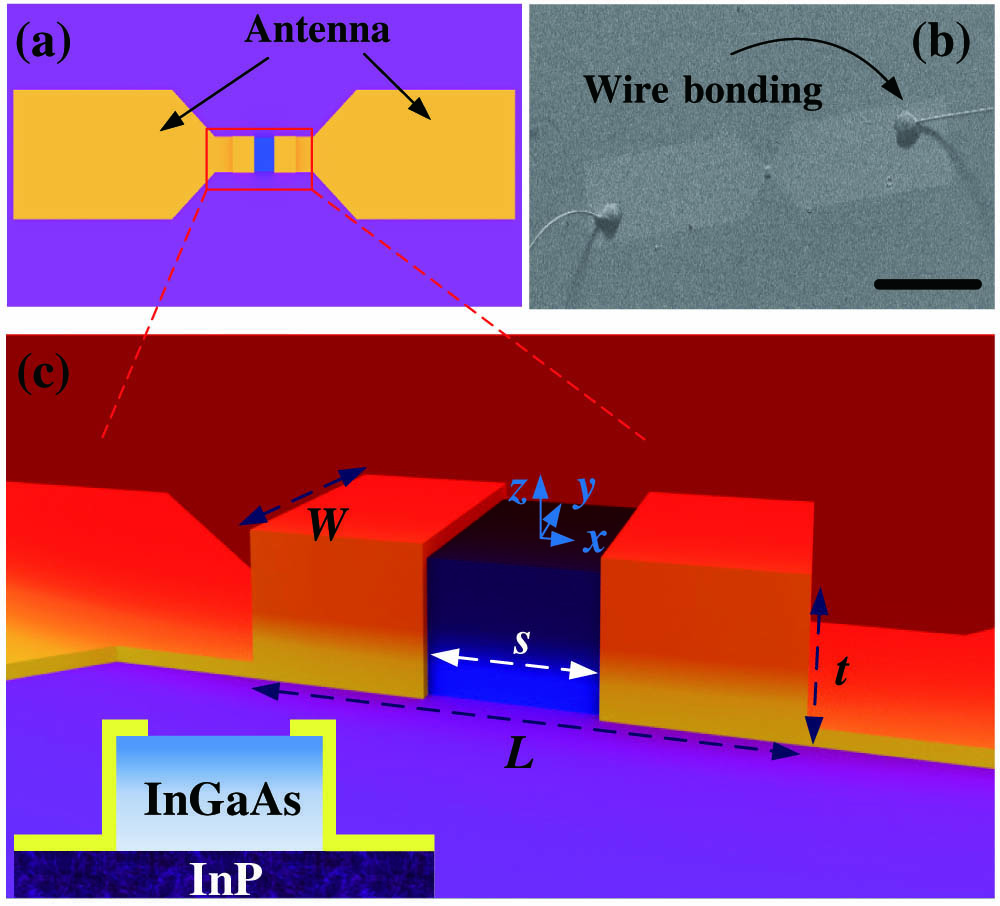
Figure 1.Schematic of the antenna-assisted subwavelength ohmic Au–InGaAs–Au photodetector (not drawn to scale). (a) Full view of the schematic of the photodetector. (b) Scanning electron microscope image of the fabricated device with wire bonding. The scale bar represents 1 mm. (c) The zoom in tridimensional view for the central part of the structure. is the length of the semiconductor, and is the spacing between the edges of the two ohmic contacts. and are the width and thickness of the InGaAs layer, respectively. The left-bottom inset is the cross section of the detector.
InGaAs is a well-known III–V semiconductor that is commonly used as an interband transition-based photodetection material for the near-infrared (NIR) range, with both photoconductive and photovoltaic architectures [28]. It has been maturely used as focal planar arrays in the NIR range. It is lattice matched to the InP substrate when the component of indium is approximately 0.53, which offers a good material quality and capability of large-scale wafer growth. The metal organic chemical vapor deposition grown in our work has a bandgap of , an electron concentration of , and an electron mobility of at room temperature. The substrate is 350 μm SI InP (100) doped with Fe. The resistivity is . The plasma frequency of is near 3.2 THz, which is in the terahertz wave range and allows negative permittivity below it [25,29]. The planar antenna depicted in Fig. 1 is configured as a half-wave dipole designed for a specific wavelength () [30]. It is worth noting that this detection strategy based on InGaAs is quite different from the InGaAs-based [31] (GaAs [10,11] or Ge [32]) indirect terahertz photoconductive antennas, where low-temperature-grown InGaAs (GaAs or Ge) with large resistivity and ultra-short carrier lifetime is required; however, the quality of such materials cannot be guaranteed as they require complicated defect-engineering processes, which makes them not mass-producible [33]. A local femtosecond laser is also equipped to excite photoconductive carriers. Here, the photoresponse comes directly from irradiation of millimeter and terahertz waves without assistance of the local laser. This, to the best of our knowledge, novel direct-detection methodology simplifies the device architecture and enables the fabrication of large detection arrays. Compared to the semiconductors (InGaAs, GaAs, Ge) used in conventional THz-PCs, the InGaAs here has negative permittivity to allow generation of localized SPPs; moreover, it possesses high electron mobility to allow fast transportation and collection of nonequilibrium electrons.
B. Device Simulation, Fabrication, and Characterization
To demonstrate the localized-SPP generation in our proposed devices, we did simulations for the device. The finite element method (Comsol, RF module) was used to simulate the localized-SPP generation. In the frequency range of interest, the free electrons in the conduction band of InGaAs behave as classic solid-state plasma, and the complex permittivity is given by the Drude model , where is the permittivity in vacuum, the high-frequency permittivity is indicated by , and the charge carrier average collision rate is indicated by () [34]. The plasma frequency is defined as , where is the electron density, is the elementary charge, and is the effective electron mass [28,35]. The plasma frequency can be derived as 3.2 THz. Gold (Au/Sn) can be regarded as a perfect conductor in such a long wavelength range. The complex permittivity of the InP substrate was taken from published data [36].
First, we did simulations on a single bare InGaAs slice [air–InGaAs–air structure, Fig. 1(a)] to study the normal localized-SPP generation in InGaAs before we configured it into a real device architecture. The simulated InGaAs slice has a length () of 150 μm, a width () of 50 μm, and a thickness () of 3 μm. The radiation frequency of a TM-polarized plane wave (with the electric field in the -direction) is set as 0.0375 THz for facilitating performance testing experimentally by our equipment. As shown, the localized-SPP intensity indicated by is very weak inside the InGaAs strip but becomes very strong at the two interfaces between InGaAs and air, which is in accordance with the fact that when SPPs are excited, they mainly exist in the dielectric layer (air in this case) [26]. To let the structure become a practically measurable device, we need to add metal contacts in the structure. Therefore, we simulated the subwavelength Au–InGaAs–Au structure (the effects of the very thin adhesion Sn layer were neglected here) without a planar couple antenna [Fig. 1(b)] by coating an Au layer on two sides, which covers part of the InGaAs strip surface, separated by a spacing () of 90 μm. With the assistance of the perfect conductor (Au), it is observed that the SPP intensity still reaches the peak value at the two same interfaces of the spacing; however, compared to the bare InGaAs, inside the InGaAs strip, the SPP intensity becomes a little larger. These simulation results confirm the excitation of SPPs in the subwavelength structure, but the intensity () is very small, resulting in insufficient generation of nonequilibrium electrons. To further increase the localized-SPP intensity, a planar Au antenna with a half-wave dipole-like configuration [37] designed for is added to the structure. The simulation results for this antenna-assisted structure [Fig. 1(c)] with the same Au–InGaAs–Au dimensions as before still show a similar SPP distribution, but with an obvious increase in the intensity of localized SPPs inside the InGaAs strip. As shown, the intensity of at the interface reaches , indicating strong excitation of SPPs.
We then did a simulation for this antenna-assisted subwavelength Au–InGaAs–Au structure (the final detector structure) to get the result of SPP intensities for different powers of the same incident source [Fig. 2(d)]. In the simulation, the value of at the position (, 0, 0) is chosen as the indication of localized-SPP intensity. It is observed that the SPP intensity is in a positive linear relation with the power because the increasing number of incident photons can result in more SPPs being generated. Figure 2(e) simulates the effects of the polarization angle of incident radiation on the SPP intensity in the device. As shown, with the polarization angle of the incident light changing from the -axis (TM configuration) to the -axis [transverse electric (TE) configuration], the SPP intensity gradually decreases from the peak to valley point, and it shows the periodic variation with the angle. This is understandable as the antenna is designed with this polarization dependence on incident light, and it can couple more TM-polarized radiation. To investigate the influence of spacing on the SPP intensity, we then simulated the localized-SPP intensity distributions in devices with fixed and , but with varied values of spacing [Fig. 2(f)]. Based on the simulation results, we can observe that the peak value of SPP intensity always exists at the interfaces of Au and InGaAs, and this value increases as the spacing decreases, indicating stronger generation for SPPs in narrower gaps. It can also be found that inside the InGaAs strip, the SPP intensity decays exponentially with distance, and it is negligible in the gold layer, which is in agreement with the previous report of the localized-SPP characteristics. Besides, we can observe that the SPP intensity is very close to zero inside the InGaAs strip for the large-spacing condition, and it experiences an increasing trend as the space decreases. According to the above observations, we can obtain the preliminary conclusions that the generation of localized SPPs occurs at the interfaces of Au and InGaAs and that it experiences fast decay with distance into the InGaAs strip. With sufficiently large spacing, the SPPs inside the InGaAs strip, especially in the middle, are negligible and SPPs mainly exist near the interfaces. However, as the spacing decreases, the distribution of SPPs can be extended into the InGaAs strip, even in the middle. Therefore, we can deduce that the superposition of the SPPs originating from the Au–InGaAs interfaces leads to the generation of SPPs in the middle of the InGaAs strip, and the intensity of SPPs in the middle could increase when the superposition becomes stronger, that is, the spacing decreases.

Figure 2.Numerical simulations for the antenna-assisted subwavelength Au/Sn–InGaAs–Au/Sn structure. Excitation of localized SPPs, the distribution of along the white dashed line for the incident radiation of in (a) the bare InGaAs slab (, , and ), (b) the subwavelength Au/Sn–InGaAs–Au/Sn structure (the same InGaAs slab with ), and (c) the antenna-assisted subwavelength Au/Sn–InGaAs–Au/Sn structure with . (d) Localized-SPP intensity () of the device in (c) as a function of incident power at 0.0375 THz. (e) SPP intensity of the device at different polarization angles for irradiation of 0.0375 THz at the point (, 0, 0). (f) SPP intensity along the half-width line for devices with spacings of 10, 30, 50, 70, 90, and 110 μm. Inset: as a function of .
In device fabrication, the parameters follow the designs in simulations. The InGaAs sample was first rinsed sequentially by acetone, isopropyl alcohol, and deionized water. Standard ultraviolet photolithography was then used to define the slab. After chemical solution etching (dihydroxysuccinic acid: ), a series of strips with a width () of 50 μm and a thickness () of 3 μm, but with different lengths (), was formed. Then, photolithography was conducted a second time to define the metallic contact and planar antenna. Finally, the planar antenna-assisted subwavelength devices with a spacing varying from 10 μm to 110 μm (in consistent with simulation) were completed through the standard e-beam evaporation and lift-off processes. The metallic antennas in experiments include 20 nm Sn (adhesion layer) followed by 300 nm Au to allow good ohmic contact. The device with a log-period antenna has the same fabrication process but different pattern design. The photoresponse measurements were done in the system shown in Fig. 3. As the power limit of millimeter and terahertz sources and our simple OMSM structure, we test the AC response of the photodetectors with mechanically or electrically modulated incident radiation, depending on the modulation frequency. The device was biased by a direct current (DC) and illuminated from the front side. The photovoltage signal generated by the detector is documented by the lock-in amplifier or an oscilloscope after a preamplifier. We used an Agilent E8257D microwave source combined with a horn as the radiation source for radiation from 0.03 THz to 0.04 THz, and an electronic frequency doubling source (Virginia Diodes Inc.) as the signal for 0.164–0.175 THz. A Golay cell was used to calibrate the incident power onto the device.
Figure 3.Schematic of the optical measurement setup.
3. RESULTS
We first tested the device with a spacing () of 90 μm, a width () of 50 μm, and a thickness () of 3 μm, as well as an Au antenna with a length of 4 mm [designed for () radiation], a width of 0.5 mm, and a thickness of 300 nm. The current–voltage (I–V) characteristic of the device was measured in the range of to 0.2 V [inset of Fig. 4(a)], and excellent symmetric and ohmic behavior was observed, ruling out asymmetrical coupling of radiation and the existence of Schottky barriers. To demonstrate the photoresponse of the device to millimeter-wave radiation, we then measured the photovoltage of the device using the 0.0375 THz radiation source. Figure 4(a) shows the photovoltage as a function of biased DC current, measured with the source output power of at a modulation frequency of 2000 Hz. Significant photovoltage was indeed observed, and it increased with the bias current. The photovoltage is about 0.15 μV at a bias of 0.5 mA and increases to 0.4 μV at 2 mA. The photovoltage is described as , where is the photocurrent, is the InGaAs strip resistance, is InGaAs strip cross-sectional area for current flow, is the nonequilibrium electron density induced by localized SPP, is the elementary charge, is the electron mobility in the strip, and is the electrical field associated with the bias. Normally, spreads in a non-uniform manner along the length of the InGaAs strip. However, for the low-bias current and fixed incident power, the , as well as other parameters, can be treated as constants at specific positions, except , which increases linearly with bias. Therefore, under the condition of low-bias current, shows a linear increasing trend with the bias current, mainly because of the increased electrical field [38]. This photovoltage dependence on the bias current is similar to conventional photoconductors.
Figure 4.Characterization of the antenna-assisted subwavelength Au/Sn–InGaAs–Au/Sn devices. (a) Photovoltage of the device with under 10 mW illumination of a 0.0375 THz source at a modulation frequency of 2000 Hz, as a function of DC bias current. Inset is a typical I–V characteristic curve of the device. The derived resistance is . (b) Photovoltage of the same device as a function of source output power at 2000 Hz under a DC bias of 2 mA. (c) Polarization dependence of the photovoltage of the device measured under a DC bias of 2 mA and at the source output power of 10 mW. The vertical and horizontal axes are designated as and , respectively. (d) Photovoltages of devices with different values of spacing, measured in the same conditions as for the device with a spacing of 90 μm.
The photovoltage also has a linear relationship with the source output power for the tested range up to 15 mW [Fig. 4(b)], which is consistent with the simulation results shown in Fig. 2(d). This is because more incident radiation excites more SPPs, which in turn generate more conducting nonequilibrium electrons for the photocurrent. This typical linear dependence also demonstrates the single photon process in this novel detection [39]. The polarization dependence of the photovoltage for the 0.0375 THz source measured at 2000 Hz under a DC bias current of 2 mA, shown in Fig. 4(c), is also in agreement with the simulated results [see Fig. 2(e)]. The photovoltage (or SPPs) reaches the largest value when the polarization is along the -axis (TM), decreases as the polarization deviates from the -axis, and finally disappears when the polarization is along the -axis (TE). This polarization dependence is mainly determined by the coupling of a dipole-like antenna and the SPP generation in InSb. To study the effects of the spacing on the detector performance, devices with spacing ranging from 10 μm to 110 μm were also fabricated and tested. As shown in Fig. 4(d), with the spacing decreasing, the photovoltage significantly increases. For the device with the minimum (10 μm) spacing, the photovoltage increases to 3.8 μV, approximately 10 times that of the 90 μm spacing device. This observation differs from the phenomenon in traditional photodetectors, where the photovoltage has a positive relation with the semiconductor area [27]. It is reasonable to observe this discrepancy since in traditional photodetectors, the photogenerated carriers are generated from interband or intraband transitions in the semiconductor, whereas in our proposed devices, the semiconductor InGaAs layers act as the medium for localized-SPP excitation and SPP-induced nonequilibrium electron transition under a specific bias.
We also characterized the spectral response of the device at approximately the designed frequency range of the antenna. As shown in Fig. 5(a), the photoresponse shows a very obvious peak at the expected frequency. For extending the photodetection to other frequency ranges, we also fabricated a device with a log-period antenna designed for [inset of Fig. 5(b)] [40]. As shown in Fig. 5(b), the photovoltage indeed exhibits a peak at the expected frequency. Therefore, by changing the resonant frequency of the coupling antenna, the photodetector can detect the desired radiation provided that SPPs can still be excited. This is similar to other types of terahertz photodetectors; although based on different detection mechanisms, all of them need a properly designed antenna to couple the radiation into the detecting structures [33,41,42]. We also measured the spectral response of the device for radiation near the bandgap energy of the semiconductor for reference. As shown in Fig. 5(c), the response has a cutoff frequency at approximately 182 THz, close to the bandgap of , which is far away from the new detectable frequency ranges.
Figure 5.Relative spectral response of the devices in a different frequency range (normalized value). Response of the device designed for (a) and (b) . The red lines in (a) and (b) are for a better view. The inset of (b) is the schematic of the log-period antenna device. The red arrow represents the polarization direction of the electric field component of incident light. (c) Response of the device shown in (b) under radiation at around the bandgap energy of the InGaAs semiconductor. The arrow indicates the cutoff (bandgap) of .
To obtain the response speed of the device, we measured the photoresponse of the device with a half-wave dipole-like antenna at a different modulation frequencies. Figure 6(a) shows the typical response waveform of the device under the illumination of 0.0375 THz radiation with a modulated frequency of 2000 Hz. Figure 6(b) [derived from Fig. 6(a)] demonstrates that the rise time (10% up to 90% of the maximum value) of the device is approximately 45 μs. Figure 6(c) (top panel) presents the normalized photovoltage signal with respect to the modulation frequency up to 100 kHz, that is, the amplitude–frequency response of the device. As shown, the photovoltage does not decrease significantly until the modulation frequency up to . The [43] (the signal decreased to 70.7% of the maximum) of the device is approximately 7200 Hz, corresponding to a rise time (signal from 0 to 63.2% of the maximum here) of 49 μs according to [44], which is very close to the speed directly derived from the response waveform [Fig. 6(b)]. To make a comparison, we also measured the response speed of the thermal Golay cell (widely used commercial terahertz detector, TYDEX), and its and are 15 Hz and 23 ms, respectively. Thus, the response speed of the device is almost three orders of magnitude faster than that of the commercial thermal Golay cell. The transit time for the conductive nonequilibrium electrons can be estimated by , where is the spacing of the device, and is the drift velocity of nonequilibrium electrons. It is approximately 54 ns for the detector with . The RC constant of the antenna can be estimated to be approximately . The two values are far less than the measured response speed of 45 μs, likely due to the large RC constant of the measurement setup.
Figure 6.Performance of the device for the 0.0375 THz detection at room temperature. (a) Typical response waveform of the device with a spacing of 90 μm at a modulation frequency of 2000 Hz. (b) A single-period responding waveform of the device. The rise time is defined as the amplitude rising from 10% to 90% of the peak value. (c) Typical bandwidth and its corresponding rise time for the Au–InGaAs–Au device (top panel) and commercial Golay cell (bottom panel) derived from the amplitude–frequency response. (d) Responsivity and NEP of the device with the spacing of 90 μm at different DC current biases. (e) Responsivity and NEP of devices with spacing varying from 10 μm to 110 μm at a DC current bias of 2 mA.
By using a calibrated Golay cell, the responsivity of the device can be expressed as , where and are the output voltage of the device and Golay cell, respectively, is the power density, is the antenna effective absorption area, expressed as ( indicates the gain of the antenna) [45], is the absorption area of the Golay cell (), and is the responsivity of the Golay cell ( at 15 Hz). In experiments, the output voltage of the Golay cell for 0.0375 THz radiation was 34.5 mV, and the calibrated was . The (in the front-illumination direction) calculated by a high frequency structure simulator was 1.73. NEP, defined as the lowest detectable power in a 1 Hz bandwidth, can be described as , where is the root mean square of the noise voltage, and is the detector voltage responsivity. For our detectors, besides the thermal Johnson–Nyquist noise (), which usually plays the dominant role in terahertz FETs, the noise due to bias (, dark current) also plays an important role in our device. Therefore, the total noise can be expressed as [14], where is the Boltzmann constant, is the thermodynamic temperature of the detector, is the device resistance, is the elementary charge, and is the dark current (bias current in our case). At the bias for the device with spacing of 90 μm, the calculated noise is , which is very close to the noise measured by a spectrum analyzer. The derived responsivity and NEP of the device with the spacing of 90 μm are shown in Fig. 6(d). The responsivity of this device is approximately 2.8 V/W under the applied DC current bias of 2 mA, and a corresponding NEP of can be achieved. We also obtain the performance of devices with different spacing. With the decrease of the device spacing, we can observe the improvement of both the responsivity and NEP of the device, as shown in Fig. 6(e). The results agree with the simulations and suggest that the SPP intensities, and hence the non-equilibrium electron concentration at the interface and within the whole spacing, become higher as the spacing decreases. The performance of the device is reasonably expected to be further improved by further shrinking the size of spacing owing to the increased intensity of the SPP generation. In experiments, for the 10 μm device, its responsivity and NEP can reach 25 V/W and , respectively. This performance is superior to commercial pyroelectric and Golay cells, and comparable to the Schottky diode. A detailed comparison of the device room temperature performance between this work and the state of the art is presented in Table 1.
| Devices | NEP (W·Hz−1/2) | Frequency (THz) | Speed |
| Golay cells [6] | 10−10–10−9 | 0.02–20 | 25 ms |
| Pyroelectric [6] | 10−9 | 0.1–3 | 10 ms |
| Schottky diodes [46] | 10−12 | 0.06–1.5 | <ns |
| Si FET [47] | 10−10 | <0.7 | – |
| THz PC [12] | – | 0.1–1.5 | <ns |
| Graphene [14] | 10−9–10−8 | 0.3 | – |
| Black phosphorus [18] | 10−8 | 0.3 | – |
| InGaAs | 10−11 | 0.0375; 0.166 (depending on antenna) | 54 μs |
Table 1. Comparison of Room Temperature Performance to the State of the Art
To explore the real application of the novel terahertz detector, we built a home-made imaging system [Fig. 7(a)], where 0.166 THz radiation was utilized as the imaging source. The detector with a photoresponse at this frequency point was used as the imaging detector. A high-density polyethylene convex lens with a focal length of 100 mm was used in the imaging. The imaging objects were put on the focal plane of the focus lens. The images were acquired by raster-scanning the objects at the beam focus. The photo-signal data were automatically collected and processed by a PC controller. As shown in Fig. 7(c), we obtained the imaging with an area of at 0.166 THz for a sealed key and a sealed leaf by normal A4 papers. The sawtooth and hole on the key, the edge of the leaf, as well as the air gaps between them, can be well distinguished with a reasonable spatial resolution, which is directly related to the good signal-to-noise ratio of the detector at 0.166 THz. This can be seen from the typical response waveform of the device [Fig. 7(d)]. This imaging exploration for large-area objects is very meaningful for current millimeter and terahertz wave applications, for example, the airport security check, where shielded metals like knives and guns can be discovered by this type of imaging. The imaging outcomes show the feasibility of the InGaAs-based photodetectors for room temperature millimeter and terahertz focal planar arrays, which have a wide range of applications.
Figure 7.Room temperature imaging. (a) The schematic and real setting of transmittance-type imaging system. (b) The imaging objects are a leaf and a key, which were glued to a 3 mm polymethyl methacrylate plate with high transmittance in the imaging frequency range. (c) Image at 0.166 THz. (d) Typical photoresponse waveform of the imaging detector at 0.166 THz with a modulation frequency of 1 kHz.
4. CONCLUSION
In this work, we reported the sensitive and direct photodetection of millimeter and terahertz waves in compact antenna-assisted subwavelength ohmic metal–InGaAs–metal structures, based on localized surface plasmon-polariton-excited nonequilibrium electrons. The device architecture omits a local laser-pumping configuration in conventional THz-PCs and the complicated treble electrodes arrangement in THz-FETs. We achieved room temperature photodetection for different frequency ranges with different coupling antenna designs. The achieved noise-equivalent power of the device with a spacing of 10 μm is () at 0.0375 THz for room temperature operation. The photodetector shows a typical response speed of 45 μs. The room temperature imaging at 0.166 THz demonstrates the capability of this device for practical applications. This work extends the optoelectronic application of InGaAs beyond its bandgap limit, and the epitaxially grown InGaAs on the lattice-matched InP substrate makes it promising in developing sensitive uncooled large focal planar arrays.
References
[1] D. Mittleman. Sensing with Terahertz Radiation(2003).
[2] Q. Qin, B. S. Williams, S. Kumar, J. L. Reno, Q. Hu. Tuning a terahertz wire laser. Nat. Photonics, 3, 732-737(2009).
[3] B. Ferguson, X. C. Zhang. Materials for terahertz science and technology. Nat. Mater., 1, 26-33(2002).
[4] N. K. Grady, J. E. Heyes, D. R. Chowdhury, Y. Zeng, M. T. Reiten, A. K. Azad, A. J. Taylor, D. A. R. Dalvit, H.-T. Chen. Terahertz metamaterials for linear polarization conversion and anomalous refraction. Science, 340, 1304-1307(2013).
[5] G. Auton, D. B. But, J. Zhang, E. Hill, D. Coquillat, C. Consejo, P. Nouvel, W. Knap, L. Varani, F. Teppe, J. Torres, A. Song. Terahertz detection and imaging using graphene ballistic rectifiers. Nano Lett., 17, 7015-7020(2017).
[6] F. Sizov, A. Rogalski. THz detectors. Prog. Quantum Electron., 34, 278-347(2010).
[7] V. I. Shashkin, V. L. Vaks, V. M. Danil’tsev, A. V. Maslovsky, A. V. Murel, S. D. Nikiforov, O. I. Khrykin, Y. I. Chechenin. Microwave detectors based on low-barrier planar Schottky diodes and their characteristics. Radiophys. Quantum Electron., 48, 485-490(2005).
[8] M. Dyakonov, M. Shur. Shallow water analogy for a ballistic field effect transistor: new mechanism of plasma wave generation by DC current. Phys. Rev. Lett., 71, 2465-2468(1993).
[9] H. Qin, X. Li, J. Sun, Z. Zhang, Y. Sun, Y. Yu, X. Li, M. Luo. Detection of incoherent terahertz light using antenna-coupled high-electron-mobility field-effect transistors. Appl. Phys. Lett., 110, 171109(2017).
[10] W. Knap, Y. Deng, S. Rumyantsev, M. S. Shur. Resonant detection of subterahertz and terahertz radiation by plasma waves in submicron field-effect transistors. Appl. Phys. Lett., 81, 4637-4639(2002).
[11] C. W. Berry, N. Wang, M. R. Hashemi, M. Unlu, M. Jarrahi. Significant performance enhancement in photoconductive terahertz optoelectronics by incorporating plasmonic contact electrodes. Nat. Commun., 4, 1622(2013).
[12] K. Peng, P. Parkinson, L. Fu, Q. Gao, N. Jiang, Y.-N. Guo, F. Wang, H. J. Joyce, J. L. Boland, H. H. Tan, C. Jagadish, M. B. Johnston. Single nanowire photoconductive terahertz detectors. Nano Lett., 15, 206-210(2014).
[13] H. C. Liu, C. Y. Song, A. J. SpringThorpe, J. C. Cao. Terahertz quantum-well photodetector. Appl. Phys. Lett., 84, 4068-4070(2004).
[14] L. Vicarelli, M. S. Vitiello, D. Coquillat, A. Lombardo, A. C. Ferrari, W. Knap, M. Polini, V. Pellegrini, A. Tredicucci. Graphene field-effect transistors as room-temperature terahertz detectors. Nat. Mater., 11, 865-871(2012).
[15] J. Yan, M.-H. Kim, J. A. Elle, A. B. Sushkov, G. S. Jenkins, H. M. Milchberg, M. S. Fuhrer, H. D. Drew. Dual-gated bilayer graphene hot-electron bolometer. Nat. Nanotechnol., 7, 472-478(2012).
[16] X. Cai, A. B. Sushkov, R. J. Suess, M. M. Jadidi, G. S. Jenkins, L. O. Nyakiti, R. L. Myers-Ward, S. Li, J. Yan, D. K. Gaskill, T. E. Murphy, H. D. Drew, M. S. Fuhrer. Sensitive room-temperature terahertz detection via the photothermoelectric effect in graphene. Nat. Nanotechnol., 9, 814-819(2014).
[17] F. H. L. Koppens, T. Mueller, P. Avouris, A. C. Ferrari, M. S. Vitiello, M. Polini. Photodetectors based on graphene, other two-dimensional materials and hybrid systems. Nat. Nanotechnol., 9, 780-793(2014).
[18] L. Viti, J. Hu, D. Coquillat, W. Knap, A. Tredicucci, A. Politano, M. S. Vitiello. Black phosphorus terahertz photodetectors. Adv. Mater., 27, 5567-5572(2015).
[19] W. Tang, A. Politano, C. Guo, W. Guo, C. Liu, L. Wang, X. Chen, W. Lu. Ultrasensitive room-temperature terahertz direct detection based on a bismuth selenide topological insulator. Adv. Funct. Mater., 28, 1801786(2018).
[20] S. Komiyama, O. Astafiev, V. Antonov, T. Kutsuwa, H. Hirai. A single-photon detector in the far-infrared range. Nature, 403, 405-407(2000).
[21] J. Tong, W. Zhou, Y. Qu, Z. Xu, Z. Huang, D. H. Zhang. Surface plasmon induced direct detection of long wavelength photons. Nat. Commun., 8, 1660(2017).
[22] C. Genet, T. W. Ebbesen. Light in tiny holes. Nature, 445, 39-46(2007).
[23] W. L. Barnes, A. Dereux, T. W. Ebbesen. Surface plasmon subwavelength optics. Nature, 424, 824-830(2003).
[24] J. A. Schuller, E. S. Barnard, W. Cai, Y. C. Jun, J. S. White, M. L. Brongersma. Plasmonics for extreme light concentration and manipulation. Nat. Mater., 9, 193-204(2010).
[25] J. Tong, L. Y. M. Tobing, S. Qiu, D. H. Zhang, A. G. Unil Perera. Room temperature plasmon-enhanced InAs0.91Sb0.09-based heterojunction n-i-p mid-wave infrared photodetector. Appl. Phys. Lett., 113, 011110(2018).
[26] A. J. Hoffman, L. Alekseyev, S. S. Howard, K. J. Franz, D. Wasserman, V. A. Podolskiy, E. E. Narimanov, D. L. Sivco, C. Gmachl. Negative refraction in semiconductor metamaterials. Nat. Mater., 6, 946-950(2007).
[27] S. A. Maier. Plasmonics: Fundamentals and Applications(2007).
[28] A. Rogalski. Infrared Detectors(2010).
[29] R. J. Nicholas, J. C. Portal, C. Houlbert, P. Perrier, T. P. Pearsall. An experimental determination of the effective masses for GaxIn1–xAsyP1–y alloys grown on InP. Appl. Phys. Lett., 34, 492-494(1979).
[30] K. Moon, H. Han, I. Park. Terahertz folded half-wavelength dipole antenna for high output power. International Topical Meeting on Microwave Photonics, 2, 301-304(2005).
[31] A. Takazato, T. Matsui, J. Kitagawa, Y. Kadoya. InGaAs photoconductive antennas for THz emission and detection with 1.56 μm excitation. Conference on Lasers and Electro-Optics (CLEO), 1-2(2007).
[32] A. Singh, A. Pashkin, S. Winnerl, M. Helm, H. Schneider. Gapless broadband terahertz emission from a germanium photoconductive emitter. ACS Photon., 5, 2718-2723(2018).
[33] K. Moon, E. S. Lee, I.-M. Lee, D. W. Park, K. H. Park. Photo-conductive detection of continuous THz waves via manipulated ultrafast process in nanostructures. Appl. Phys. Lett., 112, 031102(2018).
[34] J. Lloyd-Hughes, E. Castro-Camus, M. B. Johnston. Simulation and optimisation of terahertz emission from InGaAs and InP photoconductive switches. Solid State Commun., 136, 595-600(2005).
[35] Y. A. Goldberg, N. M. Shmidt. Gallium indium arsenide phosphide (GaxIn1–xAsyP1–y). Ternary and Quaternary III-V Compounds, 2(1999).
[36] E. D. Palik. Handbook of Optical Constants of Solids II(1991).
[37] A. B. Constantine. Antenna Theory: Analysis and Design(2005).
[38] A. Takazato, M. Kamakura, T. Matsui, J. Kitagawa, Y. Kadoya. Terahertz wave emission and detection using photoconductive antennas made on low-temperature-grown InGaAs with 1.56 μm pulse excitation. Appl. Phys. Lett., 91, 011102(2007).
[39] C. Karnetzky, P. Zimmermann, C. Trummer, C. Duque Sierra, M. Wörle, R. Kienberger, A. Holleitner. Towards femtosecond on-chip electronics based on plasmonic hot electron nano-emitters. Nat. Commun., 9, 2471(2018).
[40] R. Mendis, C. Sydlo, J. Sigmund, M. Feiginov, P. Meissner, H. L. Hartnagel. Tunable CW-THz system with a log-periodic photoconductive emitter. Solid. State. Electron., 48, 2041-2045(2004).
[41] A. Zak, M. A. Andersson, M. Bauer, J. Matukas, A. Lisauskas, H. G. Roskos, J. Stake. Antenna-integrated 0.6 THz FET direct detectors based on CVD graphene. Nano Lett., 14, 5834-5838(2014).
[42] M. Venkatesh, K. S. Rao, T. S. Abhilash, S. P. Tewari, A. K. Chaudhary. Optical characterization of GaAs photoconductive antennas for efficient generation and detection of terahertz radiation. Opt. Mater., 36, 596-601(2014).
[43] E. K. Lau, A. Lakhani, R. S. Tucker, M. C. Wu. Enhanced modulation bandwidth of nanocavity light emitting devices. Opt. Express, 17, 7790-7799(2009).
[44] M. A. Klompenhouwer. 51.1: Temporal impulse response and bandwidth of displays in relation to motion blur. SID Symposium Digest of Technical Papers, 36, 1578-1581(2005).
[45] E. Castro-Camus, J. Lloyd-Hughes, M. B. Johnston, M. D. Fraser, H. H. Tan, C. Jagadish. Polarization-sensitive terahertz detection by multicontact photoconductive receivers. Appl. Phys. Lett., 86, 254102(2005).
[46] A. Semenov, O. Cojocari, H.-W. Hübers, F. Song, A. Klushin, A.-S. Müller. Application of zero-bias quasi-optical Schottky-diode detectors for monitoring short-pulse and weak terahertz radiation. IEEE Electron Dev. Lett., 31, 674-676(2010).
[47] R. Tauk, F. Teppe, S. Boubanga, D. Coquillat, W. Knap, Y. M. Meziani, C. Gallon, F. Boeuf, T. Skotnicki, C. Fenouillet-Beranger, D. K. Maude, S. Rumyantsev, M. S. Shur. Plasma wave detection of terahertz radiation by silicon field effects transistors: responsivity and noise equivalent power. Appl. Phys. Lett., 89, 253511(2006).


