In recent years, low-dimensional materials especially 2D materials have attracted wide attention due to their novel proprieties. Plenty of devices with excellent performance have been made for different applications basing on 2D materials. In order to further explore the advantages of 2D materials and integrating them into semiconductor fabrication lines, the 2D material/Si heterostructure-based photodetectors played important roles in many different domains due to their price advantage, mature manufacturing craft and good compatibility to integrated circuits.
- Journal of Semiconductors
- Vol. 41, Issue 8, 080401 (2020)
Abstract
Graphene is a single 2D sheet of carbon atoms, it has good properties such as zero bandgap, ultrahigh carrier mobility, high conductivity[
Black phosphorus (BP) is another typical 2D material. It has wide direct bandgap (0.3–2 eV) which is thickness-dependent, strong linear dichroism and high carrier mobility[
Transitional metal dichalcogenides (TMDCs) is a big family in 2D materials. Most of TMDCs have similar characteristics such as good mechanical properties, high mobility, etc. Moreover, the indirect gap bulk material will become direct gap for some TMDCs when their thickness reduce to single layer[
![]()
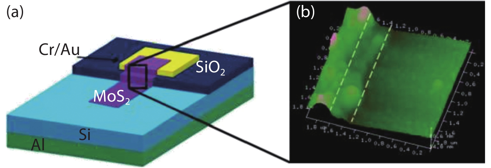
Figure 1.(Color online) (a) Schematic representations of the Si/MoS2 p–n heterojunction photodetector. (b) AFM image of MoS2 layer at metal contact and heterojunction interface[
Photodetectors based on 2D materials mentioned above had satisfying performances. However, devices of larger responsivity, higher detectivity, faster response time are still pursued by researchers. Some researchers designed the van der Waals (vdW) heterostructures made by different kinds of 2D materials. In this way, advantages of different 2D materials could be combined in one device and the lattice mismatch requirements were waived. For example, Ye et al. constructed a BP/MoS2/Si based detector and its detection range was from 532 to 1550 nm, responsivity achieved 22.3 A/W[
Owing to their outstanding performances, scientists and entrepreneurs have been working on the commercialization of 2D materials. And the best way is to integrate the 2D materials into conventional silicon-based lines. However, there are many difficulties in this process. Four critical steps: growth, transfer, encapsulation, and electric contacts are the most difficult challenges to achieve our goal. To date, graphene is one of the most commercialized product among the 2D materials. Scientists could synthesis large-scale graphene thin film with high quality on a wafer scale[
Tremendous advances have been made in the design of two-dimensional material/Si heterostructure detectors, but many challenges still exist and need to be resolved in the future. There are some fields requiring additional improvement: (1) Processability and practical application, most of reports works are manipulated by manual system, it causes a hindrance for the industrialization. (2) Further improvement of the key parameters, most of present devices can only enhance one or two aspects of the key parameters. More efforts need to be cast to improve full aspects of the devices. And it is a long-term process for all researchers.
References
[1] A C Neto, F Guinea, N M Peres et al. The electronic properties of graphene. Rev Mod Phys, 81, 109(2009).
[2] T Mueller, F Xia, P Avouris. Graphene photodetectors for high-speed optical communications. Nat Photonics, 4, 297(2010).
[3] S Lara-Avila, A Danilov, D Golubev et al. Towards quantum-limited coherent detection of terahertz waves in charge-neutral graphene. Nat Astron, 3, 983(2019).
[4] X Li, M Zhu, M Du et al. High detectivity graphene–silicon heterojunction photodetector. Small, 12, 595(2016).
[5] M Huang, M Wang, C Chen et al. Broadband black-phosphorus photodetectors with high responsivity. Adv Mater, 28, 3481(2016).
[6] F Wang, Z Wang, L Yin et al. 2D library beyond graphene and transition metal dichalcogenides: a focus on photodetection. Chem Soc Rev, 47, 6296(2018).
[7] C Gong, Y Zhang, W Chen et al. Electronic and optoelectronic applications based on 2D novel anisotropic transition metal dichalcogenides. Adv Sci, 4, 1700231(2017).
[8] V Dhyani, S Das. High-speed scalable silicon–MoS2 p–n heterojunction photodetectors. Sci Rep, 7, 44243(2017).
[9] L Ye, H Li, Z Chen et al. Near-infrared photodetector based on MoS2/black phosphorus heterojunction. ACS Photonics, 3, 692(2016).
[10] Y I Zhang, L Zhang, C Zhou. Review of chemical vapor deposition of graphene and related applications. Acc Chem Res, 46, 2329(2013).
[11] L Wang, I Meric, P Y Huang et al. One-dimensional electrical contact to a two-dimensional material. Science, 342, 614(2013).

Set citation alerts for the article
Please enter your email address


