Significance In the past half century, integrated circuits (ICs) supported by complementary metal-oxide semiconductor (CMOS) technology have developed rapidly, which promotes the continuous progress of modern information technology. As the feature size of transistors continues to decrease, the semiconductor-manufacturing process is gradually approaching its limit, resulting in slow or even stagnant improvement of integration. Meanwhile, the system performance is seriously restricted, mainly due to the electronic bottleneck. In addition, with the increase in the number of microprocessors and computing speed, power consumption and heat dissipation due to parasitic effects are becoming the main limiting factors. To break through the bottleneck of conventional IC technology in the post-Moore era, optical interconnects are considered to gradually replace conventional electrical interconnects. Compared with electrical signals, using light as the carrier for signal transmission has its unique advantages, such as large bandwidth, low loss, strong anti-electromagnetic interference capability, and high-speed parallel transmission without crosstalk. Therefore, optical interconnects will undoubtedly become the enabling technology for high-speed data transfer. Concurrently, at the network nodes, conventional optical-electrical-optical signal processing is still limited by the electronic bottleneck. Processing signals in the optical domain offer an effective strategy to increase speed. Consequently, on-chip optical interconnects and processing are paramount to the development of modern high-speed and large-capacity communication networks.
The photonic integrated circuit (PIC) is paramount to realize on-chip optical interconnects and processing, which achieves rapid development in recent years. Silicon and III-V are both promising materials for the PIC platform. The main advantage of InP and other III-V materials is that they are direct bandgap materials, which can be used to fabricate semiconductor lasers, amplifiers, modulators, detectors, and other active devices. However, the cost is relatively high and size is relatively large, which limit their large-scale commercialization. By contrast, silicon materials have distinct advantages of large reserves in nature, low cost, almost transparent in the near-infrared and even mid-infrared bands, low loss, and large refractive index contrast of silicon on insulator (SOI), making them suitable for large-scale and high-density integration. Importantly, silicon materials are fully compatible with the existing mature CMOS process, which is essential for developing silicon-based PICs. Since silicon material is an indirect bandgap material, it is impossible to produce high-efficiency light sources. Monolithic integration of all active and passive devices on a single material platform is still challenging. The hybrid integration technology provides a possible solution, which enables the integration of discrete active devices, such as lasers and amplifiers, onto silicon-based passive devices through co-packaging, epitaxial bonding, and monolithic growth to realize low-cost and high-performance hybrid PICs.
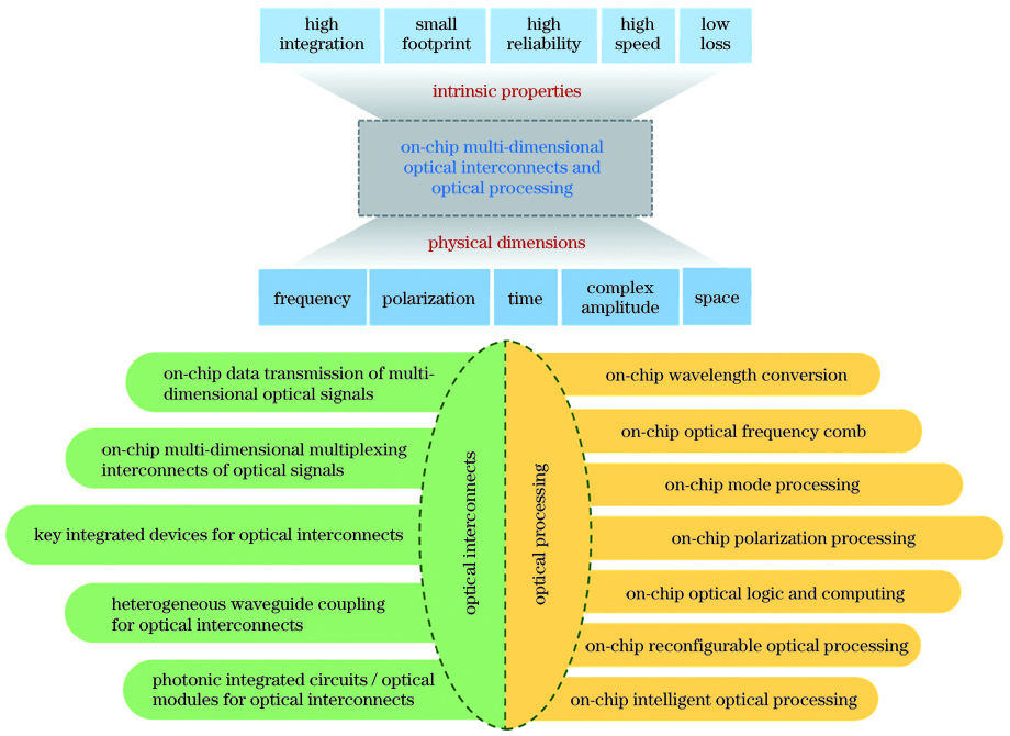
Although on-chip optical interconnects and processing are the development trends of high-speed communication networks, the sustainable increase of communication capacity is still crucial in the big data era with increasing capacity demand. Notably, photons have multiple physical dimensions, such as frequency/wavelength, polarization, time, complex amplitude, and spatial structure, which can be developed into multiple multiplexing and advanced modulation technologies, making it possible to realize ultra-high-capacity optical communications and interconnects. Wavelength-division multiplexing (WDM), time-division multiplexing (OTDM), polarization-division multiplexing (PDM), space-division multiplexing, and advanced modulation formats have rapidly developed in the past few decades, significantly increasing the transmission capacity of optical communication systems. Therefore, on-chip optical interconnects and processing should also exploit multiple physical dimensions of photons. Particularly, multiple multiplexing technologies and advanced modulation formats can be combined to effectively increase the number of signal channels and aggregate capacity of on-chip optical interconnects and processing systems.
Progress Here, we give a comprehensive review of on-chip integrated multidimensional optical interconnects and processing (
Conclusions and Prospects With the rapid development of cloud computing and data centers, on-chip integrated optical interconnects and processing have become the key technologies to break through the conventional electronic bottleneck with their unique advantages in integration, speed, bandwidth, power consumption, and multiple physical dimensions. In this article, we review the key technologies and recent progress of on-chip integrated multidimensional optical interconnects and processing. Looking to the future, one would expect the development trend toward multiple materials (III-V, silicon, silicon nitride, silica, polymer, lithium niobate, and 2D material), integrations (hybrid integration, monolithic integration, and integration of photonics and electronics), physical dimensions (frequency/wavelength, polarization, time, complex amplitude, and spatial structure), frequency bands (O+E+S+C+L+U, visible, mid-infrared, microwave, and terahertz), mediums (chip, fiber, free space, and underwater), functions (multifunction, reconfigurable, programmable, and intelligent), and applications (communications, sensing, measurement, imaging, computing, and quantum) (