
Jian Wang, Xiaoping Cao, Xinliang Zhang. On-Chip Integrated Multi-Dimensional Optical Interconnects and Optical Processing[J]. Chinese Journal of Lasers, 2021, 48(12): 1206001
- Chinese Journal of Lasers
- Vol. 48, Issue 12, 1206001 (2021)
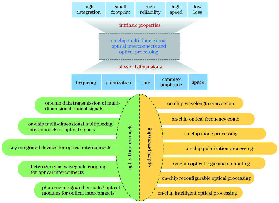
Fig. 1. Characteristics and main contents of on-chip integrated multi-dimensional optical interconnects and optical processing
![On-chip data transmission of multi-dimensional optical signals based on different types of integrated optical waveguides. (a) Strip waveguide microring resonator[21]; (b) slot waveguide[22]; (c) hybrid surface plasmon polariton (SPP) slot waveguide[23]; (d) sub-wavelength grating (SWG) waveguide[24]](/richHtml/zgjg/2021/48/12/1206001/img_2.jpg)
Fig. 2. On-chip data transmission of multi-dimensional optical signals based on different types of integrated optical waveguides. (a) Strip waveguide microring resonator[21]; (b) slot waveguide[22]; (c) hybrid surface plasmon polariton (SPP) slot waveguide[23]; (d) sub-wavelength grating (SWG) waveguide[24]
Fig. 3. On-chip multi-dimensional multiplexing interconnects of optical signals. (a) Polarization-mode hybrid multiplexing[40,32]; (b) polarization-wavelength hybrid multiplexing[41]; (c) mode-wavelength hybrid multiplexing[44]; (d)(e) wavelength-polarization-mode hybrid multiplexing[45-46]
Fig. 4. Key integrated devices of optical interconnects. (a) VCSEL array[47]; (b) high-speed direct modulation integrated vector laser[48]; (c) thin-film lithium niobate modulator[49]; (d) plasmonic modulator[50]; (e) Si-Ge avalanche photodetector (APD)[51]; (f) graphene photodetector[52]
Fig. 5. Optical coupling interfaces based on vertical coupling. (a) Vertically coupled diffractive grating structure[53]; (b) vertical coupling based on angle polished fiber[54]; (c) vertical coupling based on micro-nano optical components[55]
Fig. 6. Optical coupling interfaces based on end coupling. (a) End coupling structure[56]; (b) end coupling based on integrated polymer waveguide[57]; (c) end coupling based on in situ 3D nano-printed optical elements[58]
Fig. 7. Photonic wire bonding (PWB) technology. (a) Photonic multi-chip system based on PWB technology[59]; (b) connection between vertical emitting laser and end-coupling waveguide based on PWB technology[60]
Fig. 8. On-chip photonic integrated circuits and optical modules for optical interconnects. (a) Hybrid integrated silicon photonic ransmitter[65]; (b) fully-integrated optical transceiver network[66]; (c) coherent two-channel transceiver[67]
Fig. 9. On-chip wavelength conversion. (a)(b) Wavelength conversion using a silicon waveguide[71-72]; (c) wavelength conversion using a graphene-silicon microring resonator[73]; (d) wavelength conversion and signal regeneration using a silicon waveguide[75]
Fig. 10. On-chip optical frequency comb. (a) Optical frequency comb generation based on a microresonator[83]; (b) coherent optical communications with optical frequency combs[86]
Fig. 11. On-chip mode processing. (a) Mode spot converter[92]; (b) mode exchanger[93]; (c) multimode switch[94]; (d) OAM mode generation chip[95]
Fig. 12. On-chip polarization processing. (a) On-chip polarization analyzer[100]; (b) on-chip polarization processor[101]; (c) chiral silicon photonic circuits[102]
Fig. 13. All-optical programmable logic array based on SOA[108]. (a) Microscope image of the chip; (b) operation principle; (c) measured temporal waveforms
Fig. 14. All-optical logic gates based on PPLN[109]. (a) Experimental setup and operation principle; (b) measured temporal waveforms
Fig. 15. All-optical 2×2-bit multiplier based on HNLF[110]. (a) Operation principle; (b) measured temporal waveforms and eye diagrams
Fig. 16. M-ary optical computing based on silicon waveguides. (a) Quaternary optical computing[111]; (b) hexadecimal optical computing[112]
Fig. 17. On-chip reconfigurable and programmable optical signal processing. (a) Reconfigurable waveguide Bragg grating[113]; (b) reconfigurable waveshaper[114]; (c) programmable multi-task photonic signal processor[115]
Fig. 18. On-chip intelligent optical signal processing. (a) Automatic unscrambling of arbitrarily mixed modes in a multimode waveguide[116]; (b) self-configured reconfigurable silicon photonic signal processor[117]; (c) all-optical neural network chip architecture[119]; (d) parallel convolutional processing using an integrated photonic tensor core[120]
Fig. 19. Future development trend of optical interconnection and optical processing
Fig. 20. Basic architecture of ultra-large capacity silicon-based on-chip multi-dimensional multiplexing and processing

Set citation alerts for the article
Please enter your email address
© Copyright 2018-2021 | Chinese Laser Press. All Rights Reserved 沪ICP备15018463号-20