• Journal of Infrared and Millimeter Waves
  • Vol. 42, Issue 2, 149 (2023)
Yan-Zhen LIU, Shu-Jie LI, Ying-Xu ZHANG, Yong-Gang XIN, Zhi-Hua LI, Yang LIN, Xiong-Jun LI, Qiang QIN, Jun JIANG, and Jian-Hua GUO*
Author Affiliations
  • Kunming Institute of Physics, Kunming 650223, China
  • show less
    DOI: 10.11972/j.issn.1001-9014.2023.02.002 Cite this Article
    Yan-Zhen LIU, Shu-Jie LI, Ying-Xu ZHANG, Yong-Gang XIN, Zhi-Hua LI, Yang LIN, Xiong-Jun LI, Qiang QIN, Jun JIANG, Jian-Hua GUO. Analysis and control of abnormal phenomena in HgCdTe surface treatment[J]. Journal of Infrared and Millimeter Waves, 2023, 42(2): 149 Copy Citation Text show less
    Three typical microscopic images of water mark defects
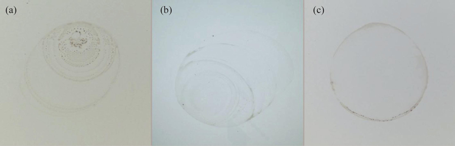
    Fig. 1. Three typical microscopic images of water mark defects
    High-resolution XPS spectra of elements with water mark defect(a),(b),(c),and normal area(d),(e),(f)
    Fig. 2. High-resolution XPS spectra of elements with water mark defect(a),(b),(c),and normal area(d),(e),(f)
    (a)Typical microscopic images of staining,(b)the response diagram,(c)the D* diagram,and(d)the noise diagram
    Fig. 3. (a)Typical microscopic images of staining,(b)the response diagram,(c)the D* diagram,and(d)the noise diagram
    XPS high-resolution spectrum of Br 3d(a),C 1s(b),and C 1s(conductive adhesive)(c)
    Fig. 4. XPS high-resolution spectrum of Br 3d(a),C 1s(b),and C 1s(conductive adhesive)(c)
    (a)Typical microscopic images of round spot,(b)the response diagram,and(c)the the number of pixels contained in the circular dark spot(a small square represents a pixel)
    Fig. 5. (a)Typical microscopic images of round spot,(b)the response diagram,and(c)the the number of pixels contained in the circular dark spot(a small square represents a pixel)
    Typical microscopic images of round spot(a)and the SEM image of material defect(b)
    Fig. 6. Typical microscopic images of round spot(a)and the SEM image of material defect(b)
    XPS high-resolution spectrum of Br 3d(a)and C 1s(b)
    Fig. 7. XPS high-resolution spectrum of Br 3d(a)and C 1s(b)
    Typical microscopic images and SEM images of normal area(a),(b),and over-roughness area(c),(d)
    Fig. 8. Typical microscopic images and SEM images of normal area(a),(b),and over-roughness area(c),(d)
    SEM images of samples after CdTe film removed for normal area(a)and over-roughness area(b)
    Fig. 9. SEM images of samples after CdTe film removed for normal area(a)and over-roughness area(b)
    SEM images of the sample without toluene immersion(a)the surface of HgCdTe,(b)the surface of CdTe,(c)the section structure of CdTe/HgCdTe,and the sample with toluene immersion(d)the surface of HgCdTe,(e)the surface of CdTe,(f)the section structure of CdTe/HgCdTe
    Fig. 10. SEM images of the sample without toluene immersion(a)the surface of HgCdTe,(b)the surface of CdTe,(c)the section structure of CdTe/HgCdTe,and the sample with toluene immersion(d)the surface of HgCdTe,(e)the surface of CdTe,(f)the section structure of CdTe/HgCdTe
    Experimental conditionsAir atmosphereN2 atmosphere
    N2 flow steady2/200/20
    N2 flow was unstable8/201/20
    Table 1. The proportion of samples with water mark defects under different experimental conditions
    Mark 1/(%)Mark 2/(%)Mark 3/(%)
    C/At13.09112.70712.872
    O/At3.2283.1213.255
    Cd/At28.82728.28730.03
    Te/At43.15142.27642.594
    Hg/At11.70313.60911.249
    Total100.000100100
    Table 2. The composition at different region
    Yan-Zhen LIU, Shu-Jie LI, Ying-Xu ZHANG, Yong-Gang XIN, Zhi-Hua LI, Yang LIN, Xiong-Jun LI, Qiang QIN, Jun JIANG, Jian-Hua GUO. Analysis and control of abnormal phenomena in HgCdTe surface treatment[J]. Journal of Infrared and Millimeter Waves, 2023, 42(2): 149
    Download Citation