• Journal of Infrared and Millimeter Waves
  • Vol. 42, Issue 2, 149 (2023)
Yan-Zhen LIU, Shu-Jie LI, Ying-Xu ZHANG, Yong-Gang XIN, Zhi-Hua LI, Yang LIN, Xiong-Jun LI, Qiang QIN, Jun JIANG, and Jian-Hua GUO*
Author Affiliations
  • Kunming Institute of Physics, Kunming 650223, China
  • show less
    DOI: 10.11972/j.issn.1001-9014.2023.02.002 Cite this Article
    Yan-Zhen LIU, Shu-Jie LI, Ying-Xu ZHANG, Yong-Gang XIN, Zhi-Hua LI, Yang LIN, Xiong-Jun LI, Qiang QIN, Jun JIANG, Jian-Hua GUO. Analysis and control of abnormal phenomena in HgCdTe surface treatment[J]. Journal of Infrared and Millimeter Waves, 2023, 42(2): 149 Copy Citation Text show less

    Abstract

    The surface treatment is the beginning of the manufacturing process of HgCdTe infrared detector chip, and its quality will directly affect the yield of the chip. The mechanisms of four typical surface anomalies in the HgCdTe surface treatment process were explored using metallographic microscope, scanning electron microscope (SEM) and X-ray photoelectron spectroscopy (XPS) analysis methods, and the corresponding control measures are proposed. The water mark defect is triggered by oxygen absorption corrosion, and this defect can be controlled by rapidly drying the HgCdTe surface with a stable nitrogen gas flow. The staining is induced by the corrosive liquid unevenly diluted or contaminated by impurities such as water. To reduce the probability of staining, the contamination should be strictly avoided in the process, and the surface should be quickly rinsed after corrosion finish. The round spot originates from the adsorption of the cleaning solution at the material defect, which can be controlled via using isopropanol to soak the HgCdTe before drying. When toluene is in direct contact with HgCdTe, the surface roughness of HgCdTe will increase, thus this direct contact should be restricted.

    Introduction

    Mercury cadmium telluride(HgCdTe)material is widely used for producing high performance cooled infrared(IR)detectors due to its specific advantages,such as the direct energy gap,ability to obtain both low and high carrier concentrations,high mobility of electrons and low dielectric constant1-2.These IR detectors are used mainly for military and high performance security applications,and have been playing more and more important roles in the construction of national defense 3-4.

    The key fabrication process of HgCdTe IR detector chip includes HgCdTe surface treatment process,ion implantation process,etching process,metallization process,indium pillar interconnection process,etc. Among them,the HgCdTe surface treatment process(including surface polishing and passivation)is very important to the chip surface/interface characteristics 5-6. If the defect density of the material after surface treatment is lower,the surface leakage current can be well suppressed7-8. HgCdTe is a ternary alloy,composed of two II-VI compounds of HgTe and CdTe,and Bromine-methanol(Br2-CH3OH)solution is usually used as polishing corrosion solution to obtain a relatively smooth surface9. After the surface of HgCdTe is freshly etched,passivation is used to minimize the effect of surface states by saturating them. Usually,a stack of both ZnS and CdTe is established for passivant10.

    However,during the fabrication of HgCdTe IR detector chip,the surface of the material is prone to local color abnormalities after finishing the surface treatment process,which will lead to the abnormal response diagram of IR detector,and some surface abnormal states will even "reappear" in the response diagram,directly leading to the scrap of the chip. Although this kind of problem is generated in many different accidental opportunities,some phenomena can still be identified through theoretical analysis and experimental verification,so as to provide guidance for controlling the emergence of these phenomena.

    Herein,four kinds of typical surface anomalies encountered in the fabrication of HgCdTe IR focal plane detector chip in Kunming Institute of Physics were analyzed and studied,namely,water marks,staining,round spot and over-roughness,and the corresponding control measures are put forward.

    1 Experiments

    The Hg1-xCdxTe(x≈0.3)samples used for this investigation were grown by liquid phase epitaxy(LPE)on the lattice-matched CdZnTe substrate. The surfaces were chemically polished with Br2-CH3OH solution(0.2%-0.5% Br2:CH3OH)by immersing the sample into the solution(dip etching),and a surface region of approximately 0.4 μm thickness was removed. Then,these samples were washed with CH3OH for several times,carefully rinsed in deionized(DI)water and blown dry with nitrogen(N2). After surface polishing,the CdTe(4 000 Å)and ZnS(3 000 Å)films were deposited by magnetron sputtering system.

    The morphology of these samples was investigated by metallurgical microscope(OLYMPUS ols 5 100)and scanning electron microscopy(SEM,FEI Quanta 200 FEG).X-ray photoelectron spectroscopy(XPS)was carried out on a Thermo K-Alpha XPS spectrometer(Thermo Fisher Scientific)equipped with a monochromatic Al Kα X-ray source( =1 468.6 eV). The six elements of Te,Cd,Hg,C,O,and Br were detected in each sample,and the Handbook of X-ray photoelectron spectroscopy was used as the basis for inspection/determination.

    2 Results and discussions

    2.1 Water marks

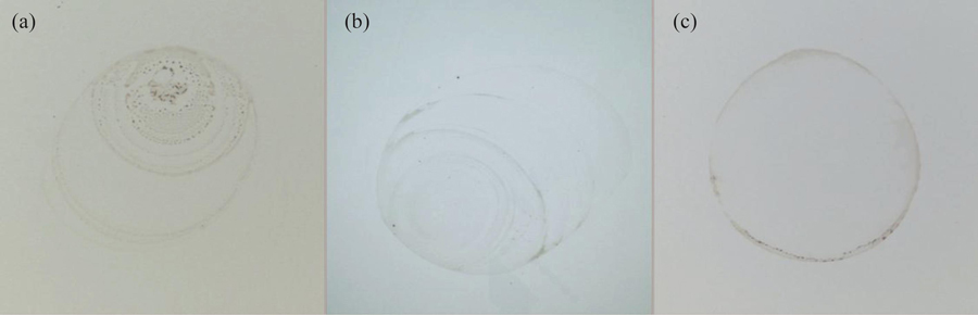
    During the HgCdTe wet etching process by Br2-CH3OH solution,although HgTe bond is much weaker than CdTe,CdTe is more unstable in etching solution due to its lower value change in the free energy. Additionally,the etching rates of the three components of HgCdTe are Cd>Hg>Te. The free energy of Te2- oxidized to soluble cations is relatively high,which can only be oxidized to Te0 by Br2. The slower etching rate of Te will lead to the HgCdTe surface rich in elemental tellurium 11-13. During the cleaning process,water droplets are easily formed on the surface of HgCdTe owing to the Te0-rich surface is hydrophobic,which will induce poor drying and form water mark defects in the N2 purge process,as shown in Fig. 1. Water mark defects could compromise adhesion to passivation film,weakening the passivation effects.

    Three typical microscopic images of water mark defects

    Figure 1.Three typical microscopic images of water mark defects

    The purity of DI water used in washing process is extremely high and consequently there is no residue when the water is evaporated. Therefore,the formation of water mark defects is not caused by the precipitation of impurities in DI water. In order to interpret the mechanism of the formation of water mark defects,XPS measurements were performed for the water mark defect and the normal area far from the water mark defect. There were no differences observed in the high-resolution spectrum of the Hg and Cd between the two test areas,as shown in Fig. 2. Figures 2(c)and(f)exhibit the high-resolution spectrum of the Te for the two test areas. We noticed a significant difference in the amount of TeO2,and the amount in the water mark defect(27.49%)is larger than that of the normal area(17.16%). The TeO2 in the normal area resulted from the oxidation of neutral Te,and the additional TeO2 in the water mark defect indicates that the formation of water mark defect is the HgCdTe oxidized. Considering the characteristics of the whole process,the most likely oxidizing agent triggers this oxidation reaction is O2 in the air 14. Nevertheless,the occurrence of water mark defects is accidental. Therefore,we explored the influence factor during HgCdTe surface drying process on the occurrence probability of water mark defects through investigating the drops of water on the HgCdTe dried in air atmosphere and N2 atmosphere respectively.

    High-resolution XPS spectra of elements with water mark defect(a),(b),(c),and normal area(d),(e),(f)

    Figure 2.High-resolution XPS spectra of elements with water mark defect(a),(b),(c),and normal area(d),(e),(f)

    The statistical results are shown in Table 1,and the number of samples in each group was 20. If the drying process completed quickly in air atmosphere with the N2 flow steady,the proportion of HgCdTe samples with water mark defects was only 2/20;On the contrary,if the N2 flow was unstable and the purge time was longer,the proportion of HgCdTe samples with water mark defects increased significantly to 8/20. In addition,when the HgCdTe samples were dried in a nitrogen atmosphere,the proportion of samples with water mark defects was 0/20 when the purge process completed quickly with the N2 flow steady. Even when the purge time was longer and the N2 flow was unstable,the proportion of samples with water mark defects was 1/20.

    Experimental conditionsAir atmosphereN2 atmosphere
    N2 flow steady2/200/20
    N2 flow was unstable8/201/20

    Table 1. The proportion of samples with water mark defects under different experimental conditions

    Based on the above experimental results,it is easy to form water mark defects on the surface of HgCdTe when the N2 flow is unstable and the purging time is longer in the atmosphere containing oxygen. The fluctuation of N2 pressure on the surface of the HgCdTe resulting from unstable N2 flow tends to induce the formation of water droplets. If the water droplets cannot be blown dry in time,they are inclined to form water trace defects in the process of slow evaporation 15. However,water is often used as the cleaning agent after wet etching of HgCdTe,and no obvious oxidation reaction occur when HgCdTe samples are immersed in water in air. Therefore,the formation mechanism of water mark defects should be oxygen absorption corrosion. In the process of oxygen absorption corrosion,the oxygen transport rate has a great influence on the reaction. At the edge of the water droplet,that is,at the solid-gas-liquid three-phase interface of air on the surface of water HgCdTe,the water content is less,and the dissolved oxygen concentration is higher. The water layer in the center of the water drop is the thickest. In the process of reaction,oxygen in the air is added more slowly by dissolution and diffusion than at the edge of the water drop,which will cause the difference in the concentration of dissolved oxygen between the center and the edge of the water drop,thus forming the concentration difference corrosion battery. The cathodic reaction is O2+2H2O+4e-=4OH-,which is mainly concentrated in the edge region of oxygen-rich water droplets. Oxygen can be quickly replenished from the air,and the generated OH- reacts with Te0 in this area as follows:3Te+6OH-=2Te2-+TeO32-+3H2O,and the generated Te2- and TeO32- can further combine with Cd2+ and Hg2+ to form corresponding compounds. The excess OH- can also combine with Cd2+ and Hg2+ to form insoluble hydroxides or oxide precipitation(Cd2++2OH-=Cd(OH)2↓,Hg2++2OH-=Hg(OH)2=HgO↓+H2O). The anodic reaction is 2H2O+Te-4e-=TeO2+4H+,which mainly occurs in the central area of water droplets. With the evaporation of water,the reaction products in water droplets precipitate on the surface of HgCdTe,and obvious water trace rings appear on the edge of water droplets. Therefore,in the surface treatment process,the simplest method to inhibit the formation of water mark defects is to use steady N2 flow to quickly dry the HgCdTe surface before the O2 dissolved into the water droplets.

    2.2 Staining

    When the surface of HgCdTe was chemically polished by Br2-CH3OH solution,the abnormal phenomenon of some areas staining,commonly known as corrosion patchy,would occasionally occur. Figure 3(a)shows a typical staining phenomenon. These stained films have a direct impact on the pixel response signal in this area,resulting in the “reappear” of irregular imprints in the response diagram(Fig. 3(b)). XPS detection method was used to analyze the element composition of the irregular imprint area,and the test results showed that in addition to Hg,Cd,and Te elements,Br element was also examined,as shown in Fig. 4. According to the XPS high resolution spectrum of C element,the proportion of each oxidation state of carbon element detected in the sample is similar to the conductive adhesive background,so the carbon element detected in the sample may only come from the conductive adhesive. Therefore,the formation of the staining phenomenon should be caused by the uneven etching of different parts by Br2 in the wet etching process. According to Fig. 3(b),the pixel response signal in staining area is ~632 mV,while the pixel response signal in normal area is ~694 mV,demonstrating that the former is 62 mV smaller than the latter. Additionally,it can be found that there is no significant difference between the areas with and without staining both in the spectral detectivity(D*)diagram(Fig. 3(c))and the noise diagram(Fig. 3(d)),indicating that the staining phenomenon has little effect on the dark current of the device. Thus,the reason for the difference in response between the areas with and without staining is the difference in quantum efficiency of pixels caused by the staining. There are more impurities on the HgCdTe surface of the area with the staining than the other area,which will make the reflection coefficient of the light incident on the lower surface different after passing through the absorption layer,thus affecting the absorption of optical signals by pixels in this area,resulting in low quantum efficiency of pixels.

    (a)Typical microscopic images of staining,(b)the response diagram,(c)the D* diagram,and(d)the noise diagram

    Figure 3.(a)Typical microscopic images of staining,(b)the response diagram,(c)the D* diagram,and(d)the noise diagram

    XPS high-resolution spectrum of Br 3d(a),C 1s(b),and C 1s(conductive adhesive)(c)

    Figure 4.XPS high-resolution spectrum of Br 3d(a),C 1s(b),and C 1s(conductive adhesive)(c)

    It was found through experimental research that when the etching process finished,the staining phenomenon exhibits a higher probability if the speed of methanol washing on the surface was slower or the surface washing agent was not uniform. In these two cases,the residual corrosion solution on the surface of HgCdTe is not uniformly diluted,which will lead to the change of the concentration gradient of etch agent in different areas,resulting in the difference of etching rates.Additionally,it was found that staining tends to form under the condition of Br2-CH3OH solution contaminated by water. Theoretically,the process of wet etching of HgCdTe by Br2-CH3OH is chemical corrosion,and Br2 molecules directly collide with the surface of HgCdTe to generate corrosion products. However,when there are impurities such as water in the solution,these impurities act as the electrolyte of ionic conductor,and the electrochemical reaction preferably proceed between HgCdTe and the corrosion solution. At this time,the electrochemical inhomogeneity on the surface of the HgCdTe,including surface chemical composition nonuniformity,the crystal structure inhomogeneity(such as grain and grain boundary),as well as the inhomogeneity of physical state(such as stress distribution,deformation,etc.),can result in the surface with different potential in some micro areas,inducing electrochemical corrosion. For example,the atomic energy of the defect site on the HgCdTe surface is higher than that of the non-defect site,and the defect site is preferentially corroded as an anode,resulting in the difference in the thickness of the corroded film between the defect area and the non-defect area,and showing different interference colors. Therefore,in order to reduce the probability of staining,it is necessary to avoid the uneven corrosion on different parts of the HgCdTe. Additionally,in the etching process,water contamination should be avoided strictly. When the etch process is completed,the entire HgCdTe surface needs to be washed quickly with a large amount of methanol.

    2.3 Round spot

    After the passivation film layer is prepared,round spots can be observed on the surface of some HgCdTe samples,and most of these spots are centered on a defect,which generally leads to circular dark spots in the response diagram of the device(a back-illuminated device with the scale of 640×512 pixels and the pixel center distance is 15 μm as an example),as shown in Fig. 5. The diameter of the round spot is about 90 μm,and the size of the central material defect is about 6 μm. This material defect does not cause dead pixels,as exhibited in Fig. 5(c),resulting in a smaller response signal of about 8×8 pixels(the round spot area is ~59 mV smaller than the normal area).

    (a)Typical microscopic images of round spot,(b)the response diagram,and(c)the the number of pixels contained in the circular dark spot(a small square represents a pixel)

    Figure 5.(a)Typical microscopic images of round spot,(b)the response diagram,and(c)the the number of pixels contained in the circular dark spot(a small square represents a pixel)

    To explore the cause of the round spot,after the ZnS and CdTe passivation films were removed by dry etching,the element composition at the round spot was tested by XPS technology(the test point is one 10 μm×10 μm area in the round spot that avoids the central material defect,Mark 1 in Fig. 6(a),another HgCdTe sample),and Hg,Cd,Te,Br,C,and O elements were detected. Figure 6(b)shows the SEM image of the section structure of the defect in the center of the round spot marked 2 in Fig. 6(a),illustrating that the defect originates from the HgCdTe film. Figure7 shows the XPS high resolution spectrum of Br and C elements. By comparing Fig. 7(b)and Fig. 4(c),it can be found that the C=O and C-O contents of the sample accounted for 11.3% and 30.7%,respectively,which were significantly higher than that of the conductive adhesive(7.8% and 14.4%). The difference of test results indicate that the carbon element detected in the sample comes from both the sample and the conductive adhesive,demonstrating that the C element was contained in the round spot,which can be attributed to the adsorption residue of organic liquid at the defect in the wet process. In addition,according to the process carried out,it can be inferred that Br element originates from Br2 residue during Br2-CH3OH etching process. Therefore,it can be concluded that the round spot originates from the defect tending to adsorb wet agent. In the process of wet treatment,some wet agent will adsorb and remain in the defects due to the large number of tiny pores in the defects. When passivation film deposition,the residual wet agent gradually volatilizes to the defects around forming round spot owing to the temperature increase.

    Typical microscopic images of round spot(a)and the SEM image of material defect(b)

    Figure 6.Typical microscopic images of round spot(a)and the SEM image of material defect(b)

    XPS high-resolution spectrum of Br 3d(a)and C 1s(b)

    Figure 7.XPS high-resolution spectrum of Br 3d(a)and C 1s(b)

    The CH3OH molecule has strong polarity and is easily adsorbed at the defect by electrostatic interaction. It was found that after washing the surface of HgCdTe with methanol,soaking the HgCdTe sample with isopropanol,which is less volatile and less polar than methanol,for several minutes,and then drying,could significantly reduce the probability of round spot.

    2.4 Over-roughness

    After the passivation film was prepared,another common problem is that the roughness of some areas of some HgCdTe samples is too high,which is manifested as the color is obviously dark(Fig. 8(c)). After the ZnS film removed by hydrochloric acid,the surface morphology of the over-roughness and the normal area was investigated by SEM technology,and the results are shown in Fig. 8. The surface roughness of the normal area is relatively lower,while the surface of the rough area shows obvious large particles. Table 2 presents the results of energy dispersive spectrum(EDS)in normal area(Mark 1 in Fig. 8(b)),non-particle area(Mark 2 in Fig. 8(d))and particles(Mark 3 in Fig. 8(d))in over-rough area,respectively. The results demonstrate that the components of these three areas are basically the same. Then,the CdTe film was removed by acid potassium dichromate solution and the morphology was investigated by SEM. The SEM image of normal area is relatively flat,while the surface of the over-rough area has obvious particles(as shown in Fig. 9). In general,the grains of the passivation film deposited on the surface with small roughness are uniform and compact with lower internal defects. While,the passivation film deposited on the surface with high roughness is porous and loose,showing a higher defect density. During the process of passivation film preparation,on the rough surface of HgCdTe sample,the adsorption energy of adsorbed atom varies greatly,so nuclei are tend to form at the positions with higher adsorption energies,inducing the formation of large particles. For the surface with small roughness,the distribution adsorption position is relatively uniform due to the smaller difference degree of adsorption energy,resulting in the passivation film structure more uniform and compact. Therefore,the phenomenon of over-roughness of passivation film can be ascribed to the larger surface roughness of HgCdTe in this area.

    Typical microscopic images and SEM images of normal area(a),(b),and over-roughness area(c),(d)

    Figure 8.Typical microscopic images and SEM images of normal area(a),(b),and over-roughness area(c),(d)

    Mark 1/(%)Mark 2/(%)Mark 3/(%)
    C/At13.09112.70712.872
    O/At3.2283.1213.255
    Cd/At28.82728.28730.03
    Te/At43.15142.27642.594
    Hg/At11.70313.60911.249
    Total100.000100100

    Table 2. The composition at different region

    SEM images of samples after CdTe film removed for normal area(a)and over-roughness area(b)

    Figure 9.SEM images of samples after CdTe film removed for normal area(a)and over-roughness area(b)

    It was observed that the surface roughness of HgCdTe increased significantly when it was immersed in toluene for several hours. For comparison,one HgCdTe sample with uniform surface was evenly divided into two halves and one half was soaked in toluene. Figure 10 shows the SEM images of HgCdTe samples without and with toluene immersion. The surface roughness of the HgCdTe sample without toluene immersion is small,while the sample after toluene immersion shows many large particles,which is consistent with the results in Fig. 9(b). Subsequently,CdTe film and ZnS film were deposited on two samples by conventional process,and ZnS film was removed by hydrochloric acid. Then,the morphology of the as-prepared HgCdTe samples was investigated by SEM,and the results were shown in Fig. 10(b)and(e). The surface of sample without toluene immersion is relatively flat and the particle size is small. Additionally,it can be seen from the cross section that there are a few holes in the CdTe film(Fig. 10(c)). While,there are obviously a large number of bigger particles on the surface of sample soaked in toluene(Fig. 10(e)),and these particles are embedded in the CdTe film(Fig. 10(f)),which is similar to the over-roughness phenomenon. It can be concluded that the surface roughness of HgCdTe immersed in toluene increases,which may be caused by a certain interaction between toluene and HgCdTe.

    SEM images of the sample without toluene immersion(a)the surface of HgCdTe,(b)the surface of CdTe,(c)the section structure of CdTe/HgCdTe,and the sample with toluene immersion(d)the surface of HgCdTe,(e)the surface of CdTe,(f)the section structure of CdTe/HgCdTe

    Figure 10.SEM images of the sample without toluene immersion(a)the surface of HgCdTe,(b)the surface of CdTe,(c)the section structure of CdTe/HgCdTe,and the sample with toluene immersion(d)the surface of HgCdTe,(e)the surface of CdTe,(f)the section structure of CdTe/HgCdTe

    During the preparation of HgCdTe IR detector chip,some organic impurities on the initial surface of HgCdTe should be cleaned by organic reagents,including toluene,acetone and ethanol,before surface polishing. Thus,the over-roughness problem may be due to the direct contact of toluene with the HgCdTe surface. Through the experiment,it was found that by shortening the soaking time of toluene or using trichloroethylene instead of toluene,the over-roughness problem was obviously controlled. However,the interaction mechanism between toluene and HgCdTe still needs to be further studied.

    3 Conclusions

    In summary,the water marks,staining,round spot,and over-roughness problems in the HgCdTe surface treatment process were analyzed and studied,and the corresponding control measures were put forward. The formation mechanism of water mark defects is oxygen absorption corrosion,and the simplest method to reduce the probability of this problem is by using steady N2 flow to quickly dry the HgCdTe surface before the O2 dissolved into the water droplets. The staining is resulted from by uneven dilution of the corrosion solution or contamination of the corrosion solution by water or other impurities. Therefore,it is necessary to avoid the uneven corrosion on different parts of the surface of HgCdTe and it needs to strictly avoid water contamination. The round spot is induced by the cleaning solution adsorbed at the defect during cleaning. The method to reduce the probability of this phenomenon is to soak the wafer in isopropanol for several minutes before dry N2 purge. When toluene is in direct contact with the surface of HgCdTe,the surface roughness of HgCdTe will increase. There may be a certain interaction between toluene and HgCdTe,and the direct contact between toluene and HgCdTe surface should be avoided in the process of chip preparation. These analysis of the four abnormal phenomena and the corresponding control measures can provide reference for the optimization design of HgCdTe surface treatment technology.

    References

    [1] Zhen-Hua YE, Hui-Hao LI, Jin-Dong WANG et al. Recent hotspots and innovative trends of infrared photon detectors. J. Infrared Millim. Waves 红外与毫米波学报, 41, 15-39(2022).

    [2] A Rogalski. Recent progress in infrared detector technologies. Infrared Physics & Technology, 54, 136-154(2011).

    [3] Chao-Wei YANG, Dong-Sheng LI, Li-Hua LI et al. Review of small-pixel hgcdte infrared focal plane detector. Infrared Technology, 41, 1003-1011(2019).

    [4] Rui-Jun DING, Jian-Rong YANG, Li HE et al. Development of technologies for HgCdTe IRFPA. Infrared and Laser Engineering, 49, 7(2020).

    [5] S Mallick, R Kiran, S Ghosh et al. Comparative study of HgCdTe etchants: An electrical characterization. Journal of Electronic Materials, 36, 993-999(2007).

    [6] S K Jha, P Srivastava, R Pal et al. Bake stability of CdTe and ZnS on HgCdTe: an x-ray photoelectron spectroscopy study. Journal of Electronic Materials, 32, 899-905(2003).

    [7] Xiong-jun LI, Fu-zhong HAN, Dong-sheng LI et al. A Study of Interface Electrical Characteristics for MW HgCdTe/Passivation Layer. Infrared Technology 红外技术, 37, 868-872(2015).

    [8] Lian-Jun ZHOU, Jing-Yu WANG, Li-Ping TIAN et al. Study on chemical etching of LPE HgCdTe surface. Infrared Technology 红外技术, 37, 506-509(2015).

    [9] Li-Yao ZHANG, Hui QIAO, Xiang-Yang LI. Study on bromine-methanol polishing process of HgCdTe wafers. Semiconductor Optoelectronics, 33, 683-685(2012).

    [10] Fu-Zhong HAN, Song GENG, Qi Shi et al. Passivation technology of composite film on the HgCdTe IRFPA. Infrared Technology 红外技术, 37, 864-867(2015).

    [11] V Srivastav, R Pal, B Sharma et al. Etching of mesa structures in HgCdTe. Journal of Electronic Materials, 34, 1440-1445(2005).

    [12] R Sporken, R Kiran, T Casselman et al. The effect of wet etching on surface properties of HgCdTe. Journal of Electronic Materials, 38, 1781-1789(2009).

    [13] M Seelmann‐Eggebert, G Carey, V Krishnamurthy et al. Effect of cleanings on the composition of HgCdTe surfaces. Journal of Vacuum Science & Technology B: Microelectronics and Nanometer Structures Processing, Measurement, and Phenomena, 10, 1297-1311(1992).

    [14] M Watanabe, M Hamano, M Harazono. The role of atmospheric oxygen and water in the generation of water marks on the silicon surface in cleaning processes. Materials Science and Engineering: B, 4, 401-405(1989).

    [15] J-G Park, J-H Han, S-H Kim et al. The Formation of water marks on both hydrophilic and hydrophobic wafers. MRS Online Proceedings Library (OPL, 477(1997).

    Yan-Zhen LIU, Shu-Jie LI, Ying-Xu ZHANG, Yong-Gang XIN, Zhi-Hua LI, Yang LIN, Xiong-Jun LI, Qiang QIN, Jun JIANG, Jian-Hua GUO. Analysis and control of abnormal phenomena in HgCdTe surface treatment[J]. Journal of Infrared and Millimeter Waves, 2023, 42(2): 149
    Download Citation