• Chinese Optics Letters
  • Vol. 17, Issue 2, 020010 (2019)
Jimin Shang1, Shuai Zhang2, Yongqiang Wang1, Hongyu Wen3、*, and Zhongming Wei3
Author Affiliations
  • 1School of Physics and Electronics Engineering, Zhengzhou University of Light Industry, Zhengzhou 453002, China
  • 2College of Physics and Engineering, Henan University of Science and Technology, Luoyang 471023, China
  • 3State Key Laboratory of Superlattices and Microstructures, Institute of Semiconductors, Chinese Academy of Sciences & Center of Materials Science and Optoelectronics Engineering, University of Chinese Academy of Sciences, Beijing 100083, China
  • show less
    DOI: 10.3788/COL201917.020010 Cite this Article Set citation alerts
    Jimin Shang, Shuai Zhang, Yongqiang Wang, Hongyu Wen, Zhongming Wei. Electronic and optical properties of an intrinsic type-I band alignment ZrS2/SnS2 van der Waals heterostructure for optoelectronic devices[J]. Chinese Optics Letters, 2019, 17(2): 020010 Copy Citation Text show less
    (a) Top and (b) side view of the SnS2 (ZrS2) monolayers; the primitive unit cell is represented by the dashed lines.
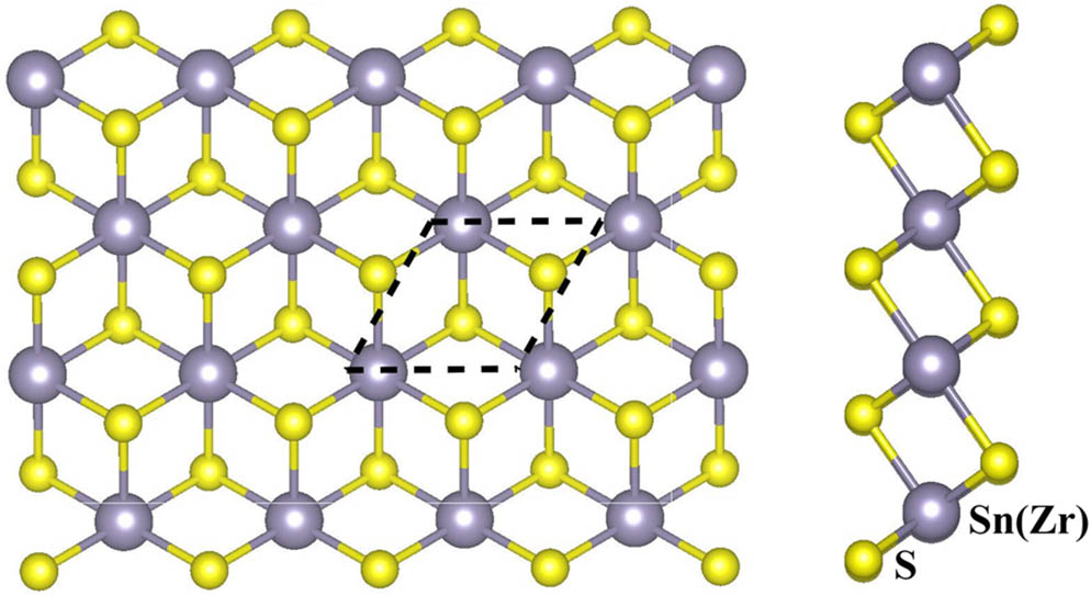
    Fig. 1. (a) Top and (b) side view of the SnS2 (ZrS2) monolayers; the primitive unit cell is represented by the dashed lines.
    Band structures and the projected density of states (PDOS) of the (a) SnS2 and (b) ZrS2 monolayers.
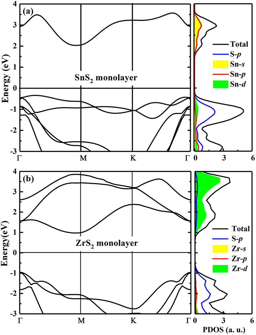
    Fig. 2. Band structures and the projected density of states (PDOS) of the (a) SnS2 and (b) ZrS2 monolayers.
    Top and side view of the AA, AB, and AC stacking of the ZrS2/SnS2 vdW heterostructure (the purple atom is Sn, the yellow atom is S, and the green atom is Zr).
    Fig. 3. Top and side view of the AA, AB, and AC stacking of the ZrS2/SnS2 vdW heterostructure (the purple atom is Sn, the yellow atom is S, and the green atom is Zr).
    (a) Projected band structure of the ZrS2/SnS2 heterobilayer. (b) The band alignments of the isolated ZrS2 and SnS2 monolayers and the heterostructure.
    Fig. 4. (a) Projected band structure of the ZrS2/SnS2 heterobilayer. (b) The band alignments of the isolated ZrS2 and SnS2 monolayers and the heterostructure.
    Optical absorption coefficient of the isolated monolayers and the heterostructure.
    Fig. 5. Optical absorption coefficient of the isolated monolayers and the heterostructure.
    (a) and (b) are the projected band structures under the electric field 0.4 V/Å and −0.4 V/Å, respectively. (c) and (d) are the relevant partial charge densities of the CBM and VBM.
    Fig. 6. (a) and (b) are the projected band structures under the electric field 0.4 V/Å and 0.4V/, respectively. (c) and (d) are the relevant partial charge densities of the CBM and VBM.
    Jimin Shang, Shuai Zhang, Yongqiang Wang, Hongyu Wen, Zhongming Wei. Electronic and optical properties of an intrinsic type-I band alignment ZrS2/SnS2 van der Waals heterostructure for optoelectronic devices[J]. Chinese Optics Letters, 2019, 17(2): 020010
    Download Citation