1School of Physics and Electronics Engineering, Zhengzhou University of Light Industry, Zhengzhou 453002, China
2College of Physics and Engineering, Henan University of Science and Technology, Luoyang 471023, China
3State Key Laboratory of Superlattices and Microstructures, Institute of Semiconductors, Chinese Academy of Sciences & Center of Materials Science and Optoelectronics Engineering, University of Chinese Academy of Sciences, Beijing 100083, China
Jimin Shang, Shuai Zhang, Yongqiang Wang, Hongyu Wen, Zhongming Wei, "Electronic and optical properties of an intrinsic type-I band alignment ZrS2/SnS2 van der Waals heterostructure for optoelectronic devices," Chin. Opt. Lett. 17, 020010 (2019)
Copy Citation Text
The electronic and optical properties of the ZrS2/SnS2 van der Waals heterostructure have been investigated. We find out that the formed heterostructure has an intrinsic type-I band alignment. Moreover, the characteristics of optical absorption in the heterostructure can be enhanced to the amount of 106 in the ultraviolet light region. In addition, the tuning electronic properties of ZrS2/SnS2 heterostructure are very interesting, due to the transitions from type-I to type-II band alignment that can occur by applying an external electric field. These results suggest that the atomically thin materials ZrS2/SnS2 heterostructure will be utilized for flexible optoelectronic applications.
In the past few years, two-dimensional (2D) semiconductor materials such as graphene and transition metal dichalcogenides (TMDs) have attracted extensive research owing to distinctive electronic and optoelectronic properties, such as suitable band gap, high carrier mobility, and high photosensitivity[1–4]. Such reviews on photodetectors have been mainly focused on 2D materials and provide new directions towards broadband photodetectors for future development[5,6]. Nevertheless, studies show that no single 2D material possesses perfect properties for practical applications, and thus constructing a van der Waals (vdW) heterostructure is used to obtain the advantages of building monolayers in experiment and theory[7,8]. Prior research shows that vdW heterostructures assembled with different 2D materials can be obtained with unique physical properties for electronic and optoelectronic devices[9–12]. In such vdW heterostructures, the in-plane stability depends on strong covalent bonds, while the stacking of different layers is held together by the vdW interactions. The existing experimental and theoretical results show that most atomically thin 2D heterostructures exhibit obvious photovoltaic effects and improvements in optical characteristics as a result of the weak interaction between the different layers. For instance, graphene/h-BN heterostructure devices present high electronic quality in new applications[13], and the ultrafast charge transfer can be found in heterobilayesr compared with isolated monolayers[14]. Due to the 2D heterostructures having great potential applications in transistors, solar cells, photodetectors, etc., more vdW heterostructures with the desired properties should be built.
As a member of the family of 2D TMDs, has been successfully fabricated using a different method. Wang et al. via an optimized chemical vapor deposition (CVD) method on traditional substrates obtained atomically thin hexagonal nanoflakes[15], and Zhang et al. reported the synthesis of hexagonal monolayer and few-layer using low-pressure CVD (LPCVD)[16]. The present results show that 2D is a promising material, and nanoelectronics based on monolayer and few-layer has good characteristics with high sensitivity and relatively high mobility.
As another typical member of the 2D layered metal dichalcogenides, nanosheet systems have attracted more attention[17,18]. Moreover, this semiconductor is abundant in the earth and environmentally friendly. Moreover, monolayer and few-layer have a band gap value of , which is larger than that for . The large band gap could show more potential modulating energy levels by strain, doping, and other methods. Recently, single and few-layer nanosheets have been employed as promising optoelectronic devices, such as field effect transistors (FETs)[17] and high-speed photodetectors[18]. Especially, Refs. [19,20] reported that the FETs based on the larger band gap of nanosheets appear with larger on/off current ratios and lower off-state leakage currents. These researches indicate that 2D and nanosheets are both competitive and promising materials for potential optoelectronic devices.
Sign up for Chinese Optics Letters TOC. Get the latest issue of Chinese Optics Letters delivered right to you!Sign up now
Here, we focus on the electronic and optical properties of the 2D vdW heterostructure because of its newly excellent properties. Moreover, there is a good lattice match between monolayer and , and it will be good for experimental fabrications, such as physical transfer technology and CVD; all can be experimentally fabricated with the 2D vdW heterostructure. Our calculations show that the vdW heterostructure owns an intrinsic type-I band alignment, where the electrons and holes are both located in the same layer[21,22]. As we know, the extensively explored TMDs heterostructures, such as [23] and [24,25], all have typical type-II band alignment from the present experimental and theoretical research. Thus, the vdW heterostructure with a type-I band alignment is still lacking[21]. In addition, the optical properties in the heterostructure are basic for optoelectronic devices. Therefore, the research about the vdW heterostructure based on type-I band alignment is necessary. Interestingly, the external electric field can effectively control the location of electrons in the vdW heterostructure. We can easily obtain a transition from type-I band alignment to type-II band alignment as a result of the tuned band offset in the heterostructure. As we know, the type-II band alignment presents the spatial distribution, where the electrons and holes are, respectively, localized in different layers, which is very beneficial to enhance the carrier life in solar cells[26–29]. The electric field effects indicate that the vdW heterostructure can become a promising candidate in photovoltaic applications.
Our simulations are carried out by employing the Vienna ab initio simulation package (VASP) code. The exchange-correlation functional is employed based on the generalized gradient approximation (GGA) within the Perdew–Burke–Ernzerhof (PBE) formula[30], and the projector-augmented wave (PAW) method[31,32] is used to replace the core electrons. We consider the vdW interactions between layers of the heterostructure using the density functional theory method of Grimme (DFT-D2), which is widely employed to reach accurate results, such as layer distances and electronic properties[33]. To more accurately calculate the band gap, Heyd–Scuseria–Ernzerhof (HSE) and GW methods are generally demanded to correct the gap values[34]. Here, the HSE06 methods are used to calculate the band structures of the monolayers in this work. Additionally, a plane-wave basis energy cutoff is fixed to 500 eV. The atomic structures are fully relaxed until the Hellmann–Feynman atomic forces on each unconstrained atom are less than 0.01 eV/Å(1 Å = 0.1 nm), and the convergence energy for electronic iterations is chosen as . The Monkhorst–Pack method in the Brillouin zone (BZ) is sampled by to obtain the electronic structure. Moreover, to avoid the interaction between layers and their periodic images, a vacuum slab of 20 Å along the axis is sufficient. The applying of the uniform electric field is disposed by adding an articial dipole sheet, which is similar to dipole correction[35]. The automatic symmetry is switched off, because the external electric field would break the inversion symmetry of the bilayer. Here, the electric field direction is vertical to the plane of the bilayer.
It is important to investigate the optical properties in optoelectronic devices. Here, the optical absorption properties are evaluated with the frequency-dependent dielectric function. The absorption spectrum can be determined by the absorption range. The optical absorption coefficient can be expressed by the following equation: in which and are the real and imaginary parts of the frequency-dependent complex dielectric function, respectively. Then, the optical absorption coefficient of the isolated monolayers and the heterostructure can be calculated from the corresponding dielectric function.
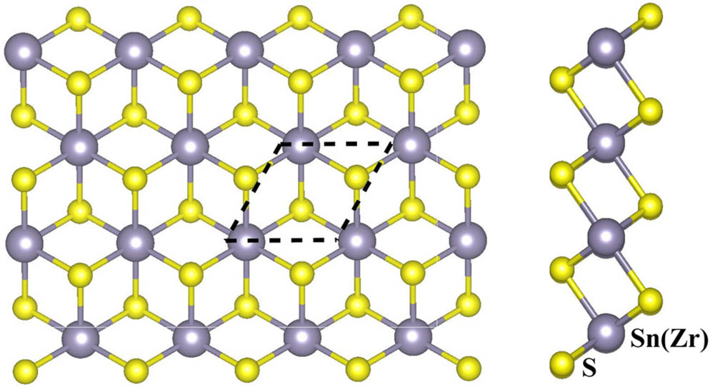
To describe the electronic properties of vdW heterostructure, we firstly consider the properties of the individual and monolayers. For bulk and , the 1T phase named -type crystals is more stable than the 2H phase[36]. Here, we adopt the widely used () bulk to build the monolayers, as shown in Fig. 1. Our optimized lattice constants are Å, and the bond length Sn-S is 2.59 Å for the monolayer; meanwhile, Å, and Zr-S is 2.58 Å for the monolayer. The lattice parameters agree well with the previous values[37,38].
Figure 1.(a) Top and (b) side view of the () monolayers; the primitive unit cell is represented by the dashed lines.
With respect to the electronic properties, as shown in Fig. 2, the projected density of states (PDOS) and band structure of the two individual monolayers are all obtained using unit cells. For the monolayer, as shown in Fig. 2(a), the conduction band maxima (CBM) lies at high symmetry point M in the BZ, while the valence band maxima (VBM) locates at the area between the high symmetry points Γ and M. The result presents the monolayer as an indirect bandgap semiconductor with the gap value of 2.61 eV from HSE06. In addition, Fig. 2(b) shows the band structures of the monolayer, where the CBM also locates at M point, and the VBM is at point, showing an indirect bandgap with value of 1.92 eV from HSE06. The present results are all consistent with other studies[39,40]. We further consider the PDOS of the two monolayers. Figure 2(a) shows that the VBM of the monolayer is mainly contributed by the orbits of the S atom and the orbits of the Sn atom, while the CBM is primarily composed of the and orbits of the Sn atom. Meanwhile, the state of the VBM in the monolayer is mainly composed of the orbits of the S atom, whereas the CBM largely consists of the orbits of the Zr atom.
Figure 2.Band structures and the projected density of states (PDOS) of the (a) and (b) monolayers.
Due to close lattice constants, here, the vdW heterostructure is built only by the unit cells of six atoms. We also examined the tiny mismatching () in the heterostructure, which has barely any effect on the electronic and optical properties of the heterostructure. To construct the vdW heterostructure through stacking the and monolayers together, here, three possible stacking patterns along the direction are considered, namely AA, AB, and AC stacking. In order to check the relative stability of these patterns, the binding energy () of the heterostructure can be, respectively, obtained using in which is the total energy of the heterostructure, and and are the total energies of the individual monolayers. Following this definition, the negative binding energy indicates that the formation of the heterostructure is more stable. The present values prove that the AA stacking is more stable than the other two patterns, although the small difference is about 67 meV. Thus, we only focus on the AA stacking in the following, as shown in Fig. 3.
Figure 3.Top and side view of the AA, AB, and AC stacking of the vdW heterostructure (the purple atom is Sn, the yellow atom is S, and the green atom is Zr).
To investigate the electronic properties of the heterobilayer, the projected band structure is described in Fig. 4(a). Compared with the results of Ref. [41], the shapes of the projected band structures calculated by PBE and HSE06 are the same, except that the band gap calculated by HSE06 is much larger. Thus, the following analyses about heterostructure are based on PBE results. It can be seen that the vdW heterostructure is an indirect semiconductor with a band gap of 0.73 eV, where the CBM still locates at M point, while the VBM locates at Γ point, similar to the isolated monolayer. Moreover, the CBM and the VBM in the heterostructure are both mainly contributed by the monolayer, as shown in the projected band structure. To further explore these spatial properties, we discuss the band alignment of the heterostructure, which is important in optoelectronic devices. Using the vacuum level () as an energy reference, the band alignment of the vdW heterobilayer is obtained. As shown in Fig. 4(b), the locations of the vdW heterostructure are compared with the isolated and monolayers. It demonstrates that the vdW heterostructure presents a natural type-I band alignment, which means that the electrons and holes are all confined in the same layers. Our results are identical to Koda’s report that the has an intrinsic type-I band alignment[41]. The light–matter interaction in the type-I heterostructure can be enhanced due to confining electrons and holes in the same layers; therefore, type-I heterostructures are mainly used in light emitting diodes[21]. In addition, the band offsets are necessary in actual optoelectronic devices. From the isolated and monolayers before contact, the valence band offset and the conduction band offset are individually and . After contact, namely in the heterostructure, the calculated valence band offset and the conduction band offset are and , respectively, which is suitable for optoelectronic devices[42]. The obvious difference of the band offset comparing the isolated monolayers and the heterostructure is due to the large charge transfer between the monolayer and the monolayer in the heterostructure.
Figure 4.(a) Projected band structure of the heterobilayer. (b) The band alignments of the isolated and monolayers and the heterostructure.
In order to discuss the potential applications of the vdW heterostructure in optoelectronic devices, we calculate the optical absorption properties of the heterostructure and the isolated monolayers. Following Eq. (1), the optical absorption coefficient is shown in Fig. 5. The absorption edge of the monolayer is smaller than that of the monolayer, which corresponds to their band gaps. For the heterostructure and the isolated monolayers, the optical absorption ranges are all broad spectrum, and the absorption peaks are many due to the different interband transitions. Especially in the ultraviolet light range, the optical absorption peaks can reach the order of for monolayers, as seen in Fig. 5. Compared with the isolated monolayers, the optical absorption peaks of the heterostructure are obviously enhanced in the ultraviolet light range, and the absorption peaks can appear at . The stronger light absorption of the bilayer can be attributed to its unique electronic structure caused by vdW interactions between layers. Thus, the enhanced optical absorption peaks in ultraviolet light band can improve the function in photoelectronic devices.
Figure 5.Optical absorption coefficient of the isolated monolayers and the heterostructure.
In practical applications, the gate voltage is useful for tuning the transition from the semiconductor to metal and the carrier density in 2D material systems[43]. In the intrinsic type-I vdW heterostructure, the electron and hole are confined in the monolayer, and thereby the recombination of the carriers is convenient. Thus, the type-I heterostructure is unfavorable for photovoltaic devices due to the lifetimes of the carriers being short. Here, we consider the effects tuned by the external vertical electric field for the vdW heterostructure. It can be seen from Figs. 6(a) and 6(b) that the effects of the external electric field are very apparent. When applying a positive electric field [0.4 V/Å, shown in Fig. 6(a)] the CBM is completely occupied by the monolayer, while the VBM is completely in the monolayer. However, when applying a negative electric field [Å, shown in Fig. 6(b)], the CBM is completely in the monolayer, and the VBM is in the monolayer. Thus, it can be seen that the type-I band alignment of the vdW heterostructures can be easily transformed into type-II band alignment under a moderate external electric field. The separation of the charge in type-II heterostructures is very suitable for in photovoltaic processes.
Figure 6.(a) and (b) are the projected band structures under the electric field 0.4 V/Å and Å, respectively. (c) and (d) are the relevant partial charge densities of the CBM and VBM.
To get further insight, here, we calculate the partial charge density of VBM and CBM in the heterostructure. As shown in Fig. 6(c), under a positive electric field 0.4 V/Å, it is clearly observed that the CBM is completely contributed by the upper layer (), while the VBM is perfectly in the lower layer ). However, for the negative electric field Å, as shown in Fig. 6(d), the CBM is perfectly in the lower monolayer, while the VBM is completely in the upper monolayer. In a word, the application of the electric field can easily achieve the separation of the CBM and VBM in different layers of the heterostructure, which can result in new potential properties in photovoltaics.
In summary, we have systematically investigated the electronic and optical properties of the vdW heterostructures using the vdW corrected DFT. The exact match between two monolayer lattices and the negative formation energies together indicate the relatively high stability of the heterostructure. For the natural vdW heterobilayer, the VBM and the CBM are all mainly confined in layers, indicating a typical type-I band alignment in heterostructures. Moreover, the excellent optical properties with strong optical peaks () can be obtained from the heterostructures in the ultraviolet region, which will improve the application of the heterostructures in optoelectronic devices. Interestingly, we realize that the intrinsic type-I band alignment in heterostructures can be transformed to type-II band alignment by applying the external vertical electric field. The charge in VBM and CBM can be perfectly separated in different layers, which will be beneficial to photovoltaic devices. The excellent properties of the heterostructures and the effective modulation under the external electric field are all essential in application. Based on the calculated electronic and optical properties, we believe that the heterostructure can be widely used in novel flexible optoelectronic devices, such as solar cells and photodetectors.
Jimin Shang, Shuai Zhang, Yongqiang Wang, Hongyu Wen, Zhongming Wei, "Electronic and optical properties of an intrinsic type-I band alignment ZrS2/SnS2 van der Waals heterostructure for optoelectronic devices," Chin. Opt. Lett. 17, 020010 (2019)