
Lingjie Fan, Maoxiong Zhao, Jiao Chu, Tangyao Shen, Minjia Zheng, Fang Guan, Haiwei Yin, Lei Shi, Jian Zi, "Full description of dipole orientation in organic light-emitting diodes," Chin. Opt. Lett. 21, 022601 (2023)
- Chinese Optics Letters
- Vol. 21, Issue 2, 022601 (2023)
Abstract
1. Introduction
Since the first reports of organic light-emitting diodes (OLEDs) in 1987[1], their efficiency has been improved through finding novel phosphorescent materials[2–10], optimizing the thickness of each layer in OLEDs[11–13], etc. In recent years, dipole orientation has also been drawing significant attention for enhancing light extraction from OLEDs[14–21].
The theory of dipole radiation in OLEDs originated from applying the theory of electrical dipoles near an interface to the problem of molecules fluorescing near a surface[22–29]. Related researches have been proposed to enhance the external quantum efficiency[30], in which the theory of the dipole orientation is developed. In previous theories, dipoles in OLEDs are decomposed into vertical dipoles and horizontal dipoles. Then, the power radiated from OLEDs is formed by weighting the power radiated by vertical dipoles and horizontal dipoles in a proportion. The weight, the ratio of vertical dipoles, can be regarded as a parameter describing the vertical orientations of the dipoles in OLEDs.
Recently, along with the OLED manufacturing progress increasingly, it is pointed out that a possible research direction of OLEDs in the future is to take advantage of the dipoles with non-uniform horizontal orientations[31,32]. Some studies point out that the carrier mobility in films using the dipoles perfectly aligning in one direction is much higher than that of films using the dipoles with uniform orientations[33,34]. At the same time, other researchers show that OLEDs with dipoles aligning in one direction can achieve the emission of linearly-polarized light. Then, the application of OLEDs directly emitting orthogonal circularly-polarized light could be realized by letting the linearly-polarized light pass through a quarter-wave plate formed by the liquid crystal[35]. Therefore, the non-uniform horizontal dipole orientation is of great significance for external quantum efficiency, as well as polarization. However, previous works have so far only considered the dipoles in OLEDs with non-uniform vertical orientations and lack of the description of the horizontal component.
Sign up for Chinese Optics Letters TOC. Get the latest issue of Chinese Optics Letters delivered right to you!Sign up now
Here, we develop a theory that fully describes the dipole orientation and its relationship with power density. Compared with the previous theory, we start from a dipole and consider an orientation distribution function, expressed as a Fourier series, to extend the power density of a dipole to the power density of the dipoles in OLEDs. Theoretically, it is the first time, to the best of our knowledge, to strictly prove that only three orientation parameters are needed to fully describe the effect of dipole orientation on the power density and extend previous orientation parameters. Two parameters describe the ratios of the
2. Methods
2.1. Power density of a dipole in OLEDs
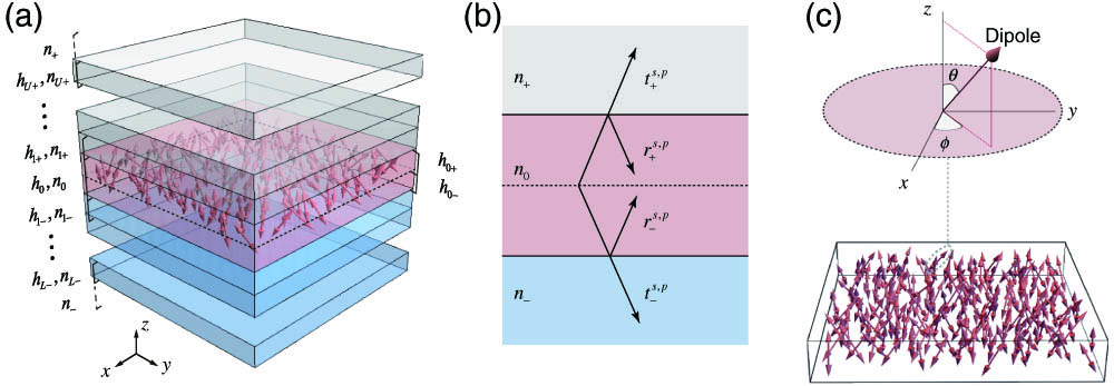
For the multi-layer model shown in Fig. 1(a), the emitting layer with refractive index
![]()
Figure 1.(a) Multi-layer films for modeling OLEDs. (b) Energy reflection and transmission coefficients of multi-layer films. (c) Upper panel: the orientation of a dipole. Lower panel: dipole orientations in layer 0.
For an electric dipole in the emitting layer with orientation (
For an emission angle
2.2. Power density of the dipoles in OLEDs
For dipole orientations in OLEDs shown in Fig. 1(c) lower panel, we can use an orientation distribution function
By using the Fourier series expansion, the orientation distribution function
Then, the orientation distribution function in the form of the Fourier series is substituted into Eq. (6). Due to the angular dependence relation of the power density of a dipole, as shown in Eq. (4), and also because the integral values of the product of two orthogonal trigonometric functions are all zero, only four Fourier components and coefficients are left among these integrations of the Fourier series. The orientation distribution function can be simplified to the orientation distribution function with four Fourier coefficients, given by
The power density per solid angle of the dipoles in OLEDs, for an emission angle
3. Results
3.1. Orientation parameters
The power density
Here, we define the orientation parameters
Thus, the power density of the dipoles in OLEDs could be written in a form of orientation parameters
In the case that there are
Considering Eqs. (13) and (9), the orientation parameters
Equation (16) verifies the physical meaning of the orientation parameters
![]()
Figure 2.Physical meaning of the orientation parameters vx, vz, and vx,z. Left panel: the dipole vector is decomposed along the y axis and x–z plane. Right panel: the dipole vector in the x–z plane is further decomposed along the x and z axes.
3.2. Structure design
To extract the orientation parameters of the dipoles in OLEDs[38,39], non-polarized spectra should be used, and different components of the power density
![]()
Figure 3.Test structure designed for extracting the orientation parameters (left panel). The refractive indices of the glass substrate and organic thin film are 1.524 and 1.72, and the emission wavelength is 500 nm. A hemispherical prism, whose refractive index is the same as the substrate, is along the glass substrate side. Simulated non-polarized power densities of the test structure (h0 = 20 nm) with different orientations (right panel).
By adjusting the thickness of organic thin film
![]()
Figure 4.Determining thickness h0 of the test structure for extracting orientation parameters vx, vz, and vx,z. (a)–(d) Simulated different components of the power densities
Non-polarized spectra with different orientation parameters, when the thickness of the organic layer is 160 nm, are shown in Fig. 5. These simulated results show that the orientation parameters proposed in our theory do cause significant difference on the spectra and could be used for extracting orientation parameters from the spectra. Here, we further explain these differences of each orientation parameter from the perspective of the dipole radiation pattern, showing the consistence with our dipole orientation theory. For an electric dipole, it hardly radiates along the direction of its dipole vector, as the orientation of the dipole vector tends to be parallel to the
![]()
Figure 5.Simulated spectra with different orientation parameters and thickness h0 of the test structure at 160 nm. Simulated spectra with different parameters vz (red lines), vx = 0.5, and vx,z = 0. Simulated spectra with different parameters vx (yellow lines), vz = 0, and vx,z = 0. Simulated spectra with different parameters vx,z (blue lines), vz = 0.5, and vx = 0.5.
3.3. Parameter retrieval
We simulated radiation of 1000 dipoles with different orientations in the test structure (
![]()
Figure 6.Results of orientation parameter retrieval. (a) Orientation distribution of 1000 simulated dipoles, which has a Gaussian distribution centered at θ = 80° and ϕ = 200° (left). The four Fourier components of this distribution (middle). The calculated orientation parameters by Eq. (
4. Conclusions
By introducing an orientation distribution function to extend the power density of a dipole to the power density of the dipoles in OLEDs, it is the first time, to the best of our knowledge, to strictly prove that only three orientation parameters are needed to fully describe the relationship between the dipole orientations and the power density. These three orientation parameters could adjust the ratio of different components of the power density. Therefore, the orientation parameter can be extracted from the power density of the dipoles in OLEDs.
We design a test structure with the thickness of organic layer
References
[1] C. W. Tang, S. A. VanSlyke. Organic electroluminescent diodes. Appl. Phys. Lett., 51, 913(1987).
[2] H. Nakanotani, T. Higuchi, T. Furukawa, K. Masui, K. Morimoto, M. Numata, H. Tanaka, Y. Sagara, T. Yasuda, C. Adachi. High-efficiency organic light-emitting diodes with fluorescent emitters. Nat. Commun., 5, 4016(2014).
[3] Y.-H. Kim, H.-C. Jeong, S.-H. Kim, K. Yang, S.-K. Kwon. High-purity-blue and high-efficiency electroluminescent devices based on anthracene. Adv. Funct. Mater., 15, 1799(2005).
[4] D. H. Kim, A. D’Aléo, X. K. Chen, A. Sandanayaka, D. Yao, L. Zhao, T. Komino, E. Zaborova, G. Canard, Y. Tsuchiya. High-efficiency electroluminescence and amplified spontaneous emission from a thermally activated delayed fluorescent near-infrared emitter. Nat. Photonics, 12, 98(2018).
[5] M. A. Baldo, D. F. O’Brien, Y. You, A. Shoustikov, S. Sibley, M. E. Thompson, S. R. Forrest. Highly efficient phosphorescent emission from organic electroluminescent devices. Nature, 395, 151(1998).
[6] M. A. Baldo, S. Lamansky, P. E. Burrows, M. E. Thompson, S. R. Forrest. Very high-efficiency green organic light-emitting devices based on electrophosphorescence. Appl. Phys. Lett., 75, 4(1999).
[7] M. G. Helander, Z. B. Wang, J. Qiu, M. T. Greiner, D. P. Puzzo, Z. W. Liu, Z. H. Lu. Chlorinated indium tin oxide electrodes with high work function for organic device compatibility. Science, 332, 944(2011).
[8] K. H. Kim, J. J. Kim. Origin and control of orientation of phosphorescent and TADF dyes for high-efficiency OLEDs. Adv. Mater., 30, 1705600(2018).
[9] R. Costa, G. Fernández, L. Sánchez, N. Martín, E. Ortí, H. Bolink. Dumbbell-shaped dinuclear iridium complexes and their application to light-emitting electrochemical cells. Chem. Eur. J., 16, 9855(2010).
[10] P. Ren, S. Wei, P. Zhang, X. Chen. Probing fluorescence quantum efficiency of single molecules in an organic matrix by monitoring lifetime change during sublimation. Chin. Opt. Lett., 20, 073602(2022).
[11] C. L. Lin, T. Y. Cho, C. H. Chang, C. C. Wu. Enhancing light outcoupling of organic light-emitting devices by locating emitters around the second antinode of the reflective metal electrode. Appl. Phys. Lett., 88, 081114(2006).
[12] M. Flämmich, M. C. Gather, N. Danz, D. Michaelis, K. Meerholz. In situ measurement of the internal luminescence quantum efficiency in organic light-emitting diodes. Appl. Phys. Lett., 95, 263306(2009).
[13] S. Nowy, B. C. Krummacher, J. Frischeisen, N. A. Reinke, W. Brütting. Light extraction and optical loss mechanisms in organic light-emitting diodes: influence of the emitter quantum efficiency. J. Appl. Phys., 104, 123109(2008).
[14] G. Chen, J. Zhu, X. Li. Influence of a dielectric decoupling layer on the local electric field and molecular spectroscopy in plasmonic nanocavities: a numerical study. Chin. Opt. Lett., 19, 123001(2021).
[15] J. Frischeisen, D. Yokoyama, C. Adachi, W. Brütting. Determination of molecular dipole orientation in doped fluorescent organic thin films by photoluminescence measurements. Appl. Phys. Lett., 96, 073302(2010).
[16] W. Brütting, J. Frischeisen, T. D. Schmidt, B. J. Scholz, C. Mayr. Device efficiency of organic light-emitting diodes: progress by improved light outcoupling. Phys. Status Solidi A, 210, 44(2013).
[17] M. Flämmich, S. Roth, N. Danz, D. Michaelis, A. H. Bräuer, M. C. Gather, K. Meerholz. Measuring the dipole orientation in OLEDs. Proc. SPIE, 7722, 77220D(2010).
[18] T. Lampe, T. D. Schmidt, M. J. Jurow, P. I. Djurovich, M. E. Thompson, W. Brütting. Dependence of phosphorescent emitter orientation on deposition technique in doped organic films. Chem. Mater., 28, 712(2016).
[19] T. Komino, Y. Oki, C. Adachi. Dipole orientation analysis without optical simulation: application to thermally activated delayed fluorescence emitters doped in host matrix. Sci. Rep., 7, 8405(2017).
[20] H. Cho, C. W. Joo, B.-H. Kwon, N. S. Cho, J. Lee. Non-linear relation between emissive dipole orientation and forward luminous efficiency of top-emitting organic light-emitting diodes. Org. Electron., 62, 72(2018).
[21] Y. Hasegawa, Y. Yamada, M. Sasaki, T. Hosokai, H. Nakanotani, C. Adachi. Well-ordered 4CzIPN ((4s,6s)-2,4,5,6-tetra(9-H-carbazol-9-yl)isophthalonitrile) layers: molecular orientation, electronic structure, and angular distribution of photoluminescence. J. Phys. Chem. Lett., 9, 863(2018).
[22] R. Chance, A. Prock, R. Silbey. Lifetime of an emitting molecule near a partially reflecting surface. J. Chem. Phys., 60, 2744(1974).
[23] W. Lukosz, R. Kunz. Light emission by magnetic and electric dipoles close to a plane interface. I. Total radiated power. J. Opt. Soc. Am. A, 67, 1607(1977).
[24] R. R. Chance, A. Prock, R. Silbey. Molecular Fluorescence and Energy Transfer Near Interfaces(1978).
[25] W. Lukosz. Theory of optical-environment-dependent spontaneous-emission rates for emitters in thin layers. Phys. Rev. B, 22, 3030(1980).
[26] W. Lukosz. Light emission by multipole sources in thin layers. I. Radiation patterns of electric and magnetic dipoles. J. Opt. Soc. Am. A, 71, 744(1981).
[27] G. Ford, W. Weber. Electromagnetic interactions with metal surfaces. Phys. Rep., 113, 195(1984).
[28] K. Neyts. Simulation of light emission from thin-film microcavities. J. Opt. Soc. Am. A, 15, 962(1998).
[29] W. Barnes. Fluorescence near interfaces: the role of photonic mode density. J. Mod. Opt., 45, 661(1998).
[30] T. D. Schmidt, T. Lampe, M. R. D. Sylvinson, P. I. Djurovich, M. E. Thompson, W. Brütting. Emitter orientation as a key parameter in organic light-emitting diodes. Phys. Rev. Appl., 8, 037001(2017).
[31] D. Yokoyama. Molecular orientation in small-molecule organic light-emitting diodes. J. Mater. Chem., 21, 19187(2011).
[32] L. Jiang, X. Luo, Z. Luo, D. Zhou, B. Liu, J. Huang, J. Zhang, X. Zhang, P. Xu, G. Li. Interface and bulk controlled perovskite nanocrystal growth for high brightness light-emitting diodes. Chin. Opt. Lett., 19, 030001(2021).
[33] V. C. Sundar, J. Zaumseil, V. Podzorov, E. Menard, R. L. Willett, T. Someya, M. E. Gershenson, J. A. Rogers. Elastomeric transistor stamps: reversible probing of charge transport in organic crystals. Science, 303, 1644(2004).
[34] T. Amaya, S. Seki, T. Moriuchi, K. Nakamoto, T. Nakata, H. Sakane, A. Saeki, S. Tagawa, T. Hirao. Anisotropic electron transport properties in sumanene crystal. J. Am. Chem. Soc., 131, 408(2009).
[35] K. Baek, D. M. Lee, Y. J. Lee, H. Choi, J. H. Kim. Simultaneous emission of orthogonal handedness in circular polarization from a single luminophore. Light Sci. Appl., 8, 120(2019).
[36] C. C. Katsidis, D. I. Siapkas. General transfer-matrix method for optical multilayer systems with coherent, partially coherent, and incoherent interference. Appl. Opt., 41, 3978(2002).
[37] L. Li. Formulation and comparison of two recursive matrix algorithms for modeling layered diffraction gratings. J. Opt. Soc. Am. A, 13, 1024(1996).
[38] L. Zhao, T. Komino, M. Inoue, J.-H. Kim, J. C. Ribierre, C. Adachi. Horizontal molecular orientation in solution-processed organic light-emitting diodes. Appl. Phys. Lett., 106, 063301(2015).
[39] T. Komino, H. Tanaka, C. Adachi. Selectively controlled orientational order in linear-shaped thermally activated delayed fluorescent dopants. Chem. Mater., 26, 3665(2014).
[40] C. A. Wächter, N. Danz, D. Michaelis, M. Flämmich, S. Kudaev, A. H. Bräuer, M. C. Gather, K. Meerholz. Intrinsic OLED emitter properties and their effect on device performance. Proc. SPIE, 6910, 691006(2008).


Set citation alerts for the article
Please enter your email address

© Copyright 2018-2021 | Chinese Laser Press. All Rights Reserved 沪ICP备15018463号-20