• Infrared and Laser Engineering
  • Vol. 52, Issue 3, 20220698 (2023)
Yingxu Zhang, Xiao Chen, Lihua Li, Peng Zhao, Jun Zhao, Xuefeng Ban, Hongfu Li, Xiaodan Gong, Jincheng Kong, Jianhua Guo, and Xiongjun Li*
Author Affiliations
  • Kunming Institute of Physics, Kunming 650223, China
  • show less
    DOI: 10.3788/IRLA20220698 Cite this Article
    Yingxu Zhang, Xiao Chen, Lihua Li, Peng Zhao, Jun Zhao, Xuefeng Ban, Hongfu Li, Xiaodan Gong, Jincheng Kong, Jianhua Guo, Xiongjun Li. Evaluation and application of HgCdTe linear avalanche focal plane devices (invited)[J]. Infrared and Laser Engineering, 2023, 52(3): 20220698 Copy Citation Text show less
    Variation of gain and excess noise factor of the HgCdTe APD with bias
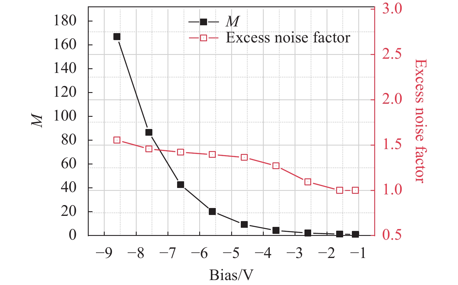
    Fig. 1. Variation of gain and excess noise factor of the HgCdTe APD with bias
    Gain grayscale map of HgCdTe APD focal plane at −8.6 V
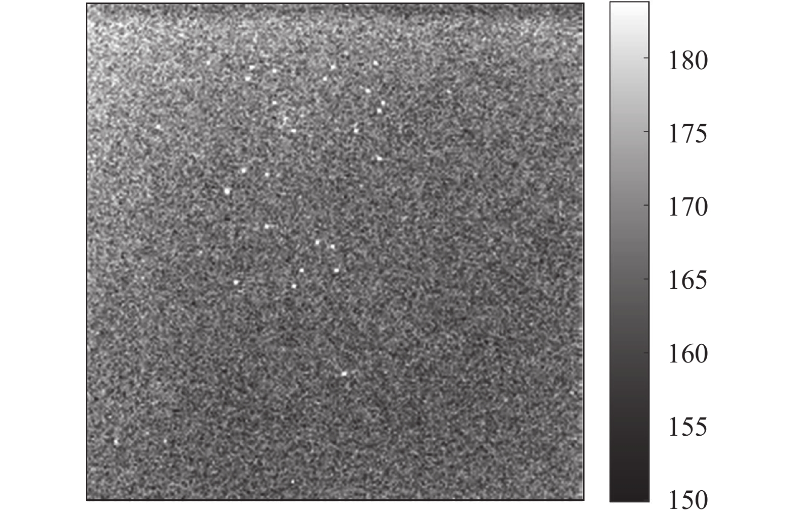
    Fig. 2. Gain grayscale map of HgCdTe APD focal plane at −8.6 V
    Excess noise factor histogram of APD focal plane at M=166
    Fig. 3. Excess noise factor histogram of APD focal plane at M=166
    Variation of NEPh with bias under different integration time
    Fig. 4. Variation of NEPh with bias under different integration time
    Schematic diagram of the noise of a APD device versus its gain
    Fig. 5. Schematic diagram of the noise of a APD device versus its gain
    Variation of excess noise factor of semiconductor APD devices with gain[17]
    Fig. 6. Variation of excess noise factor of semiconductor APD devices with gain[17]
    Schematic diagram of the thermal imaging/laser gating combined imaging system
    Fig. 7. Schematic diagram of the thermal imaging/laser gating combined imaging system
    Infrared passive and active laser combined imaging system with one detector
    Fig. 8. Infrared passive and active laser combined imaging system with one detector
    Images acquired by a dual-mode camera
    Fig. 9. Images acquired by a dual-mode camera
    Schematic diagram of readout circuit for 3D imaging
    Fig. 10. Schematic diagram of readout circuit for 3D imaging
    Schematic diagram of an active imaging system witha APD device
    Fig. 11. Schematic diagram of an active imaging system witha APD device
    Variation of photocurrent with distance without APD gain
    Fig. 12. Variation of photocurrent with distance without APD gain
    Passive mid-band infrared images obtained by Sofradir using a 320×256 (pixel spacing 30 μm) HgCdTe APD device. (a) Routine imaging,SNR=61 dB; (b) Image with short integration time, SNR=39 dB; (c) Image with high gain and short integration time, SNR=42 dB
    Fig. 13. Passive mid-band infrared images obtained by Sofradir using a 320×256 (pixel spacing 30 μm) HgCdTe APD device. (a) Routine imaging,SNR=61 dB; (b) Image with short integration time, SNR=39 dB; (c) Image with high gain and short integration time, SNR=42 dB
    Dark current variation of HgCdTe APD with bias
    Fig. 14. Dark current variation of HgCdTe APD with bias
    Passive mid-wave infrared images obtained under different gains by HgCdTe-APD. (a) M=1, the integration time is 800 μs;(b) M=1, the integration time is 20 μs; (c) M=19, the integration time is 20 μs
    Fig. 15. Passive mid-wave infrared images obtained under different gains by HgCdTe-APD. (a) M=1, the integration time is 800 μs;(b) M=1, the integration time is 20 μs; (c) M=19, the integration time is 20 μs
    Device parameterSi[19]hole-HgCdTe[20]e-HgCdTe[21]InGaAs[22]
    QE35%@ 1.06 μm >90@ 1.06 μm >83%@ 1.55 μm 80%@ 1.06 μm
    Detector cutoff/ μm 1.1SWIR4.31.2
    Bandwidth/ MHz 140500120>1000
    k(ionization ration) 0.00800.15
    Excess noise factor3~11.3-1.48@M=45
    Gain M120200-35046845
    Bias/V-161371/82.5
    NEP/ (fW/Hz1/2307-25(@M=100) 0.5150/250
    Pixel formatSingle4×42×8/64×64Single/ 16 channel
    Pixel area/μm700(dia.)-64×6475/100(dia.)
    Operating temperature/ K 300101-12084300
    Table 1. Performance comparison of different types of linear mode APD detectors reported publicly
    Array technologyFPA format and pitch/μm Frame rate/Hz Operating temperature ROIC noiseSpectral range and QE
    Intevac,InGaAs/ InP EBCMOS 640×480/13.4<30−40-20 ℃1 e/pixel@M=200 QE≥25%@1.55 μm 0.95-1.65 μm
    CEA/Leti,HgCdTe APD320×256/301500≤200 K3-4 e/pixel@M=10 QE>50%;0.2-3.0 μm
    DRS,HgCdTe APD640×480/25<12080 K1-2 e/pixel@M=70 QE>50%;0.5-4.5 μm
    Table 2. Performance comparison of APD avalanche devices fabricated from different material[20]
    ρtτaτopticLp/μm DR/mm Lf/mm R/km θL/mrad
    0.10.970.63028.38555
    Table 3. System parameters
    Yingxu Zhang, Xiao Chen, Lihua Li, Peng Zhao, Jun Zhao, Xuefeng Ban, Hongfu Li, Xiaodan Gong, Jincheng Kong, Jianhua Guo, Xiongjun Li. Evaluation and application of HgCdTe linear avalanche focal plane devices (invited)[J]. Infrared and Laser Engineering, 2023, 52(3): 20220698
    Download Citation