
Jiabing Lu, Zesheng Lv, Xinjia Qiu, Shiquan Lai, Hao Jiang. Ultrasensitive and high-speed AlGaN/AlN solar-blind ultraviolet photodetector: a full-channel-self-depleted phototransistor by a virtual photogate[J]. Photonics Research, 2022, 10(9): 2229
- Photonics Research
- Vol. 10, Issue 9, 2229 (2022)
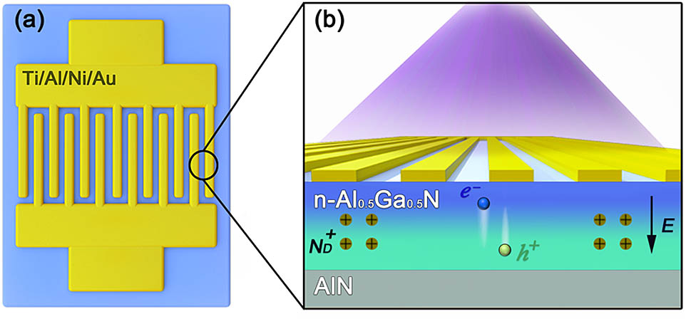
Fig. 1. Schematic diagram of Al 0.5 Ga 0.5 N / AlN Al 0.5 Ga 0.5 N
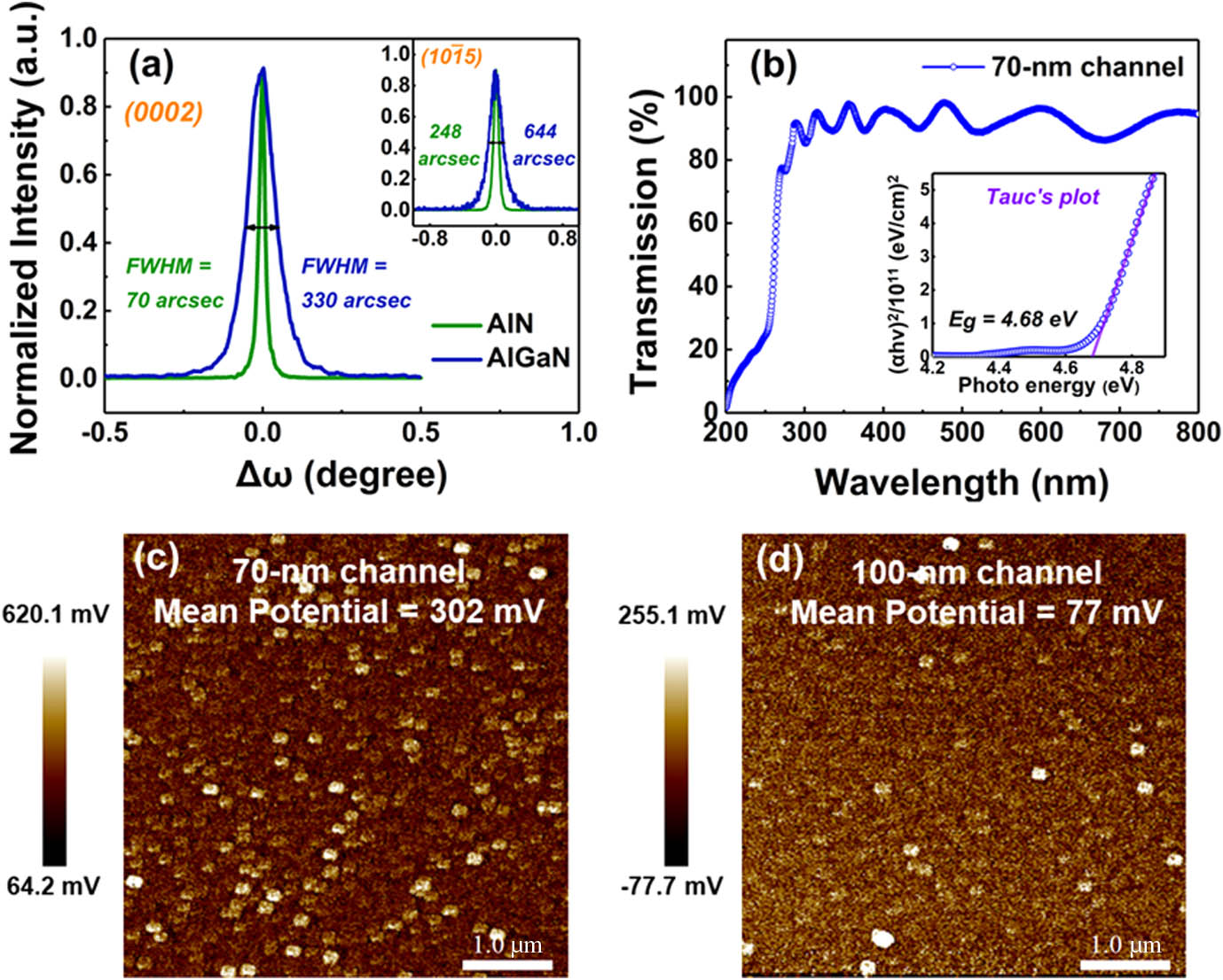
Fig. 2. (a) (0002) plane and (10 1 ¯ 5 ω -scan curves of the epitaxial sample with the 70-nm-thick n - Al 0.5 Ga 0.5 N n - Al 0.5 Ga 0.5 N 5 μm × 5 μm 256 × 256
Fig. 3. Dark and illuminated I–V curves of the n - Al 0.5 Ga 0.5 N / AlN
Fig. 4. Photoresponse characteristics of the FCSD phototransistor. (a) Spectral responses at different bias voltages. (b) Bias dependence of responsivity at 240 and 280 nm. (c) Time and irradiation intensity dependence of the response current under 5-V bias, in which the irradiation uses periodic DUV illumination with periodic on/off times of 10/20 s. (d) Transient responses to the 213-nm pulse signal with an optical power density of 127.3 mW / cm 2
Fig. 5. (a) I–V curves of the FCSD phototransistor under different incident DUV intensities. I–V curves in the bias range of 0–2 V under irradiation intensities of (b) 5.2 μW / cm 2 0.7 nW / cm 2 0.2 nW / cm 2 − 138.3 μW / cm 2
Fig. 6. (a) Schematic diagram of the neutral conductive path formed in the n-AlGaN channel of FCSD phototransistor under DUV irradiation due to the action of virtual photogate (separation of photogenerated electrons and holes). (b) Schematic diagram of energy band under dark and on illumination conditions.
|
Table 1. Summary of Key Characteristic Parameters of Solar-Blind UV Photodetectors Based on Different Materials in This Work and Previous Literatures

Set citation alerts for the article
Please enter your email address
© Copyright 2018-2021 | Chinese Laser Press. All Rights Reserved 沪ICP备15018463号-20